

Page 1

101 Innovation Drive
San Jose, CA 95134
(408) 544-7000
www.altera.com
Stratix II GX PCI Express
Development Board
Reference Manual
Document Version: 1.0.1
Document Date: April 2007
Page 2

Copyright © 2006 Altera Corporation. All rights reserved. Altera, The Programmable Solutions Company, the stylized Altera logo, specific device designations, and all other words and logos that are identified as trademarks and/or service marks are, unless noted otherwise, the trademarks and
service marks of Altera Corporation in the U.S. and other countries. All other product or service names are the property of their respective holders. Altera products are protected under numerous U.S. and foreign patents and pending applications, maskwork rights, and copyrights. Altera warrants
performance of its semiconductor products to current specifications in accordance with Altera's standard warranty, but reserves the right to make
changes to any products and services at any time without notice. Altera assumes no responsibility or liability arising out of the application or use of any information, product, or service described herein except as expressly agreed to in writing by Altera
Corporation. Altera customers are advised to obtain the latest version of device specifications before relying on any published information and before placing orders for products or services.
Part Number MNL-01002-1.1
ii Development Board Version 1.0.0 Altera Corporation
Stratix II GX PCI Express Development Board Reference Manual Preliminary August 2006
Page 3

Contents
About this Manual
Revision History ......................................................................................................................................... v
How to Contact Altera ............................................................................................................................... v
Typographic Conventions....................................................................................................................... vi
Chapter 1. Introduction
General Description................................................................................................................................ 1-1
Board Features ................................................................................................................................... 1-1
Block Diagram ................................................................................................................................... 1-2
Handling the Board ................................................................................................................................ 1-3
Chapter 2. Board Components & Interfaces
Board Overview...................................................................................................................................... 2-1
Featured Device ...................................................................................................................................... 2-5
Device Support .................................................................................................................................. 2-6
I/O & Clocking Resources ............................................................................................................... 2-6
Clocking Circuitry ................................................................................................................................ 2-11
Configuration Schemes and Status LEDs ..........................................................................................2-12
JTAG Configuration ........................................................................................................................ 2-12
FPP Configuration ........................................................................................................................... 2-14
Flash Memory Configuration File Storage ............................................................................. 2-17
MAX II CPLD Configuration Controller ................................................................................ 2-18
Status and Channel Activity LEDs ............................................................................................... 2-21
General User Interfaces........................................................................................................................ 2-22
Push Button Switches (S1 Through S4) ........................................................................................ 2-22
User-Defined DIP Switch (S5) ....................................................................................................... 2-23
User LEDs (D9 Through D16) ....................................................................................................... 2-23
Configuration DIP Switch .............................................................................................................. 2-24
Board-Specific LEDs ....................................................................................................................... 2-25
FPGA Transceiver Channel Activity LEDs ................................................................................. 2-25
Power, Configuration, and Traffic Activity LEDs ...................................................................... 2-26
Standard Communication Ports ......................................................................................................... 2-27
PCI Express Edge Connector Interface (J9) ................................................................................. 2-27
Gigabit Ethernet (GigE) Interface (RJ1) ........................................................................................2-29
SFP A and B Interfaces (J6 and J7) ................................................................................................ 2-34
High-Speed Mezzanine Connectors A and B Interface ............................................................. 2-36
JTAG Interface ................................................................................................................................. 2-44
Off-Chip Memory ................................................................................................................................. 2-44
DDR2 SDRAM ................................................................................................................................. 2-44
QDRII SRAM .................................................................................................................................... 2-49
Flash Memory .................................................................................................................................. 2-52
Altera Corporation iii
Preliminary
Page 4

Contents Stratix Device Handbook, Volume 1
Temperature Sensor ............................................................................................................................. 2-54
Heat Sink and Fan ................................................................................................................................ 2-55
Power Supply ........................................................................................................................................ 2-55
Power Supply for Each Component ............................................................................................. 2-55
Components Attached to Each Power Rail ................................................................................. 2-56
Power Distribution System ............................................................................................................ 2-58
Termination ........................................................................................................................................... 2-60
DDR2 Memory ................................................................................................................................. 2-60
QDRII Memory ................................................................................................................................ 2-60
PCI Express ...................................................................................................................................... 2-60
iv Altera Corporation
Preliminary
Page 5
About this Manual
Revision History
The table below displays the revision history for the chapters in this
reference manual.
Chapter Date Version Changes Made
All August 2006 1.0.0 First publication
All April 2007 1.0.1
Added warning not to use external power supply when the Altera
®
II GX PCI Express development board is powered from the host
Stratix
computer chassis
This reference manual provides comprehensive information about the
®
Stratix®II GX family of devices and the Stratix II GX PCI Express
Altera
development board.
How to Contact Altera
For the most up-to-date information about Altera products, go to the
Altera world-wide web site at www.altera.com. For technical support on
this product, go to www.altera.com/mysupport. For additional
information about Altera products, consult the sources shown below.
Information Type USA & Canada All Other Locations
Technical support www.altera.com/mysupport/ www.altera.com/mysupport/
(800) 800-EPLD (3753)
(7:00 a.m. to 5:00 p.m. Pacific Time)
Product literature www.altera.com www.altera.com
Altera literature services literature@altera.com literature@altera.com
Non-technical customer
service
FTP site ftp.altera.com ftp.altera.com
(800) 767-3753 + 1 408-544-7000
+1 408-544-8767
7:00 a.m. to 5:00 p.m. (GMT -8:00)
Pacific Time
7:00 a.m. to 5:00 p.m. (GMT -8:00)
Pacific Time
®
Altera Corporation v
August 2006 Preliminary
Page 6
Typographic Conventions Cyclone FPGA Device Handbook
Typographic
This document uses the typographic conventions shown below.
Conventions
Visual Cue Meaning
Bold Type with Initial
Capital Letters
bold type External timing parameters, directory names, project names, disk drive names,
Italic Type with Initial Capital
Letters
Italic type Internal timing parameters and variables are shown in italic type.
Initial Capital Letters Keyboard keys and menu names are shown with initial capital letters. Examples:
“Subheading Title” References to sections within a document and titles of on-line help topics are
Courier type Signal and port names are shown in lowercase Courier type. Examples: data1,
1., 2., 3., and
a., b., c., etc.
● • Bullets are used in a list of items when the sequence of the items is not important.
■
v The checkmark indicates a procedure that consists of one step only.
1 The hand points to information that requires special attention.
c
w
r The angled arrow indicates you should press the Enter key.
f The feet direct you to more information on a particular topic.
Command names, dialog box titles, checkbox options, and dialog box options are
shown in bold, initial capital letters. Example: Save As dialog box.
filenames, filename extensions, and software utility names are shown in bold
type. Examples: f
Document titles are shown in italic type with initial capital letters. Example: AN 75:
High-Speed Board Design.
Examples: t
Variable names are enclosed in angle brackets (< >) and shown in italic type.
Example: <file name>, <project name>.pof file.
Delete key, the Options menu.
shown in quotation marks. Example: “Typographic Conventions.”
PIA
, \qdesigns directory, d: drive, chiptrip.gdf file.
MAX
, n + 1.
tdi, input. Active-low signals are denoted by suffix n, e.g., resetn.
Anything that must be typed exactly as it appears is shown in Courier type. For
example:
actual file, such as a Report File, references to parts of files (e.g., the AHDL
keyword
Courier.
Numbered steps are used in a list of items when the sequence of the items is
important, such as the steps listed in a procedure.
The caution indicates required information that needs special consideration and
understanding and should be read prior to starting or continuing with the
procedure or process.
The warning indicates information that should be read prior to starting or
continuing the procedure or processes
c:\qdesigns\tutorial\chiptrip.gdf. Also, sections of an
SUBDESIGN), as well as logic function names (e.g., TRI) are shown in
vi Altera Corporation
Preliminary August 2006
Page 7

1. Introduction
General
Description
The Stratix®II GX PCI Express development board provides a hardware
platform for developing and prototyping high-performance PCI Express
(PCIe)-based designs as well as to demonstrate the Stratix II GX device’s
embedded transceiver and memory circuitry.
With up to 16-integrated transceiver channels and support for
high-speed, low-latency memory access (via DDR2 SDRAM and QDRII
memory interfaces), the Stratix II GX PCI Express development board
provides a fully-integrated solution for multi-channel, high-performance
applications, while also using limited board space.
®
Through the use of Altera
MegaCore® functions (or other intellectual
property [IP] cores) and expansion connectors, you can enable the
inter-operability of the Stratix II GX embedded transceivers with
third-party, application-specific standard products (ASSPs) in either
point-to-point or switching and bridging applications.
Because the Stratix II GX embedded transceivers can implement the
entire PCIe interface on one device, the StratixIIGX PCIExpress
development board offers a high-bandwidth, low-latency, powerefficient PCIe solution with sufficient LEs for your applications.
To simplify the design process, Altera provides a PCIe reference design—
available from the Altera website—for use as either a design starting
point or an experimental platform. The reference design is designed and
tested by Altera engineers and distributed with the PCI Express
Development Kit, Stratix II GX Edition (ordering code:
DK-PCIE-2SGX90N).
Board Features
The board features the following major component blocks:
■ Off-chip memory
● DDR2 SDRAM
● QDRII SRAM
■ FPGA configuration
● MAX
● JTAG interface
Altera Corporation Reference Manual 1–1
August 2006 Stratix II GX PCI Express Development Board
®
II CPLD and 16-bit page mode flash memory
Page 8

General Description
■ User and board-specific interfaces
● Push-button switches
● User DIP switch
● User LEDs
● Board-specific DIP switch
● Board-specific LEDs
■ Power supply
● Power by components
● Power by rail
● Main power source, either:
• PCIe motherboard
• Laptop-style DC power supply via DC input jack
■ Communication ports
● PCIe edge connector
● High-speed Mezzanine cards
● Gigabit Ethernet
● SFP modules
● Joint Test Action Group (JTAG) header
■ Clocking circuitry
● Three high-speed clock oscillators to support Stratix II GX
transceivers and user logic:
• 100 MHz
• 155.52 MHz
• 156.25 MHz
● SMA connector for external clock input and output
Block Diagram
Figure 1–1 shows a functional block diagram of the Stratix II GX
PCI Express development board.
1–2 Reference Manual Altera Corporation
Stratix II GX PCI Express Development Board August 2006
Page 9
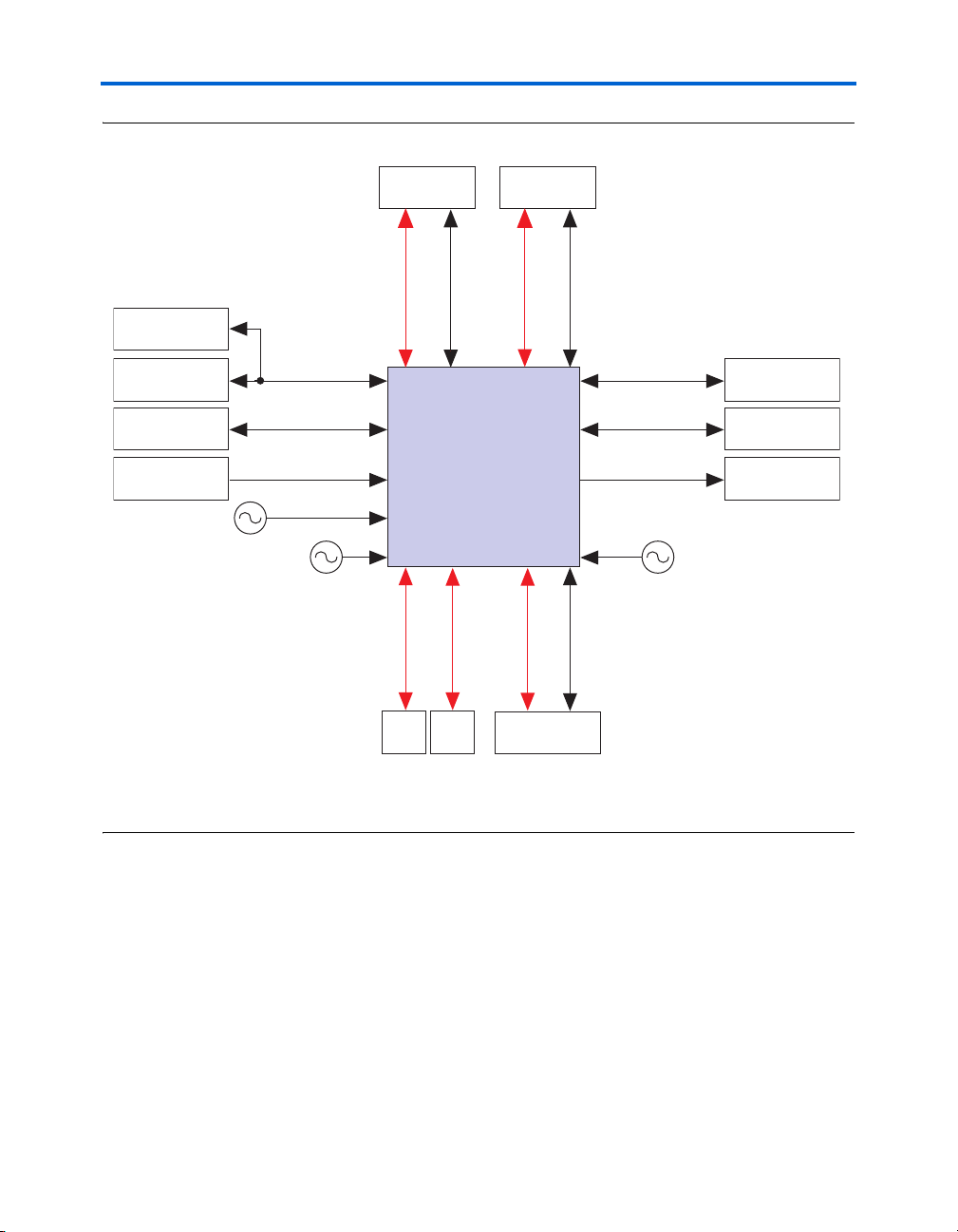
Figure 1–1. Stratix II GX PCI Express Development Board
Introduction
MAX II Device
512 MB Flash
256 MB DDR2
SDRAM (x72)
Push-Button
Switches
1.8 V/2.5 V CMOS
100.000 MHz
1.8 V CMOS
1.8 V SSTL
156.250 MHz
HMC Port A
6x XCVR
CMOS/LVDS
Stratix II GX Device
1x XCVR
1x XCVR
SFPASFP
B
HMC Port B
CMOS/LVDS
4x XCVR (1)
REFCLK
8x XCVR
x8 PCIe Edge
Connector
1.8V HSTL
1.8V HSTL
1.8V/2.5V CMOS
155.52 MHz
72 MB QDRII
(x36)
88E1111
GigE PHY+RJ45
TX/RX LEDs
User LEDs
Note to Figure:
(1) The 4x XCVR channels are only supported by Stratix II GX EP2SGX130 devices.
Handling the
When handling the board, it is important to observe the following
precaution:
Board
w Static Discharge Precaution—Without proper anti-static
handling, the board can be damaged. Therefore, use anti-static
handling precaution when touching the board.
Altera Corporation Reference Manual 1–3
August 2006 Stratix II GX PCI Express Development Board
Page 10

Handling the Board
1–4 Reference Manual Altera Corporation
Stratix II GX PCI Express Development Board August 2006
Page 11

2. Board Components & Interfaces
Board Overview
This chapter provides operational and connectivity detail for the board’s
major components and interfaces and is divided into the following major
blocks:
■ Featured device
■ Clocking circuitry
■ Configuration
■ User interface components
■ Standard communication ports
■ Off-chip memory
■ Power supply
■ Termination
1 Board schematics, the physical layout database, and
manufacturing files for the Stratix
development board are included in the PCI Express Development
Kit, Stratix II GX Edition in the following directory:
<install path>/BoardDesignFiles
®
II GX PCI Express (PCIe)
Altera Corporation Reference Manual 2–1
August 2006 Stratix II GX PCI Express Development Board
Page 12
Board Overview
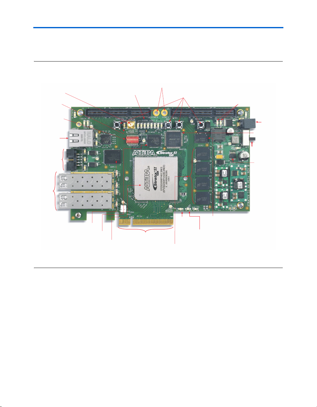
Figure 2–1 shows the top view of the Stratix II GX PCIe development
board.
Figure 2–1. Top View of the Stratix II GX PCIe Development Board
High-Speed Mezzanine
Card Interfaces A & B
External Clock Input
SMA Connector (J4)
Configuration Done
LED (D8)
User DIP Switch
Bank (S5)
Ethernet RJ-45
Single Port
(RJ1)
JTAG
Header
(J5)
SFP Ports
A and B
(J6, J7)
User LEDs
(D9 through D16)
HSMC Interface A (J1)
(J1 and J2)
User Push-Button
Switches (S1 - S4)
HSMC Interface B (J2)
Transmit/Receive
Yellow LEDs
(D5 and D6)
Power Switch
Power Supply
Input (J3)
MAX II Device
(U4)
(SW1)
Temperature
Sensor With
Alarm (U7)
DDR2 64 x 8 Mbytes
SDRAM (U2)
QDRII SRAM (U6)
Flash Device (U3)
Stratix II GX Device (U10)
PCI Express x8
Edge Connector
100-MHz
Crystal (X1)
155.25-MHz
Crystal (X4)
DDR2 32 x 16 Mbytes
SDRAM (U5, U8, U11, U13)
2–2 Reference Manual Altera Corporation
Stratix II GX PCI Express Development Board August 2006
Page 13
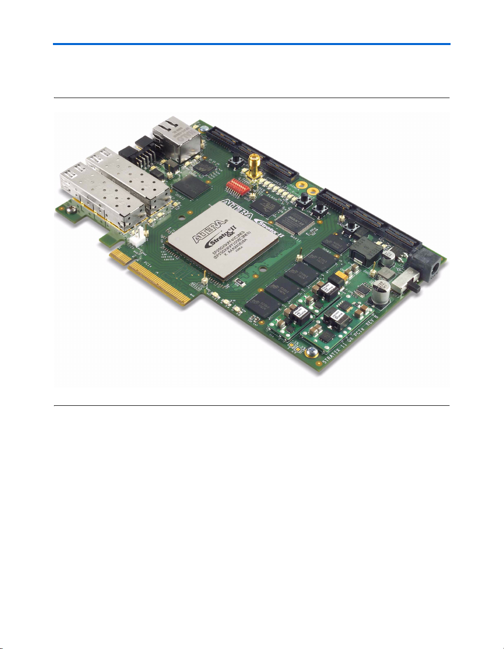
Figure 2–2 shows a diagonal view of the Stratix II GX PCIe development
board.
Figure 2–2. Diagonal View of the Stratix II GX PCIe Development Board
Board Components & Interfaces
Altera Corporation Reference Manual 2–3
August 2006 Stratix II GX PCI Express Development Board
Page 14
Board Overview
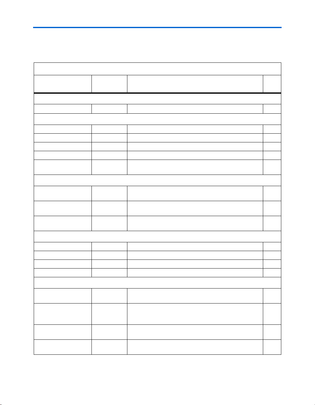
Table 2–1 describes the components and lists their corresponding board
references.
Table 2–1. Stratix II GX PCIe Development Board Features
Component/
Interface
Board
Reference
Description Page
Featured Device
Stratix II GX FPGA U10
FF1508 FPGA in a 1508-pin FineLine BGA
®
package.
2–5
Clocks
100 MHz X1 100-MHz oscillator 2–6
25 MHz X2 25-MHz crystal 2–6
156.25 MHz X3 156.25-MHz oscillator 2–6
155.52 MHz X4 155.52-MHz oscillator 2–6
SMA clock input J4 SMA connector that allows the provision of an external clock
to the Stratix II GX device’s transceivers.
2–6
Configuration and Status
Board configuration
DIP switch
Status LEDs D1, D2, D8,
Channel activity LEDs D3-D6, D17,
S6 DIP switch that controls the FPGA configuration settings. 2–23
LEDs that display power and configuration status. 2–25
D19-D22
LEDs that display RX and TX transceiver channel activity. 2–24
D18, D23-D29
User I/O
Push-button switches S1-S4 User-defined push-button switches. 2–21
User LEDs D9-D16 User-defined LEDs. 2–23
8-pin DIP switch S5 User-defined DIP switches. 2–22
JTAG header J5 10-pin header for JTAG-based FPGA communication. 2–12
Interfaces
PCIe edge connector J9 A x8 (8 channel) PCI Express edge connector for insertion
into PCI Express-based host platforms.
Ethernet RJ-45 RJ1 The RJ-45 jack is for Ethernet cable connection. The
connector is fed by a 10/100/1000 base T PHY device with a
GMII interface to the Stratix II GX device.
SFP A J6 Small form pluggable cage allows for the connection of SFP
modules.
SFP B J7 Small form pluggable cage allows for the connection of SFP
modules.
2–25
2–28
2–33
2–33
2–4 Reference Manual Altera Corporation
Stratix II GX PCI Express Development Board August 2006
Page 15
Table 2–1. Stratix II GX PCIe Development Board Features
Board Components & Interfaces
Component/
Interface
HSMC A J1 High speed mezzanine connector allows for the connection
HSMC B J2 High speed mezzanine connector allows for the connection
Board
Reference
Description Page
2–35
of HSMC daughter cards.
2–35
of HSMC daughter cards.
Memory
QDRII SRAM U6 18 Mybtes (36 bits wide by 512 Kbytes deep) of QDRII
64 x 8 Mbyte DDR2 U2, U5, U8,
U11, U13
Flash U3 512 Mbytes of flash memory. 2–16
SRAM.
256 Mybtes (72 bits wide by 32 Mbytes deep) with error
correction coding (ECC) of double data rate (DDR2)
synchronous dynamic random access memory (SDRAM).
2–48
2–44
Power
DC power jack J3 DC input connector for the board. 2–55
Power switch SW1 Switches the board’s power on or off. 2–55
Featured Device
The PCI Express Development Kit, Stratix II GX Edition features the FF1508
FPGA (U10) in a 1508-pin FineLine BGA® (FBGA) package. Table 2–2 lists
some Stratix II GX device features.
Table 2–2. Stratix II GX Features
Architectural
Feature
The Altera®
third-generation
FPGA with
embedded
transceivers
Innovative clock
management
system
Based on the
1.2-V, 90-nm
SRAM process
Altera Corporation Reference Manual 2–5
August 2006 Stratix II GX PCI Express Development Board
● Provides a robust design solution for the most popular high-speed serial interfaces
● Provides optimum jitter performance across the entire operating range of 622 Mbps to
6.375 Gbps
● Provides best-in class signal integrity performance
● Offers enhanced transmit pre-emphasis technology, programmable receiver
equalization, and output voltage control
● Clock signals are automatically routed to the appropriate destination
● Greatly simplifies high-speed board designs
● Internal clock frequency of up to 500 MHz
● Provides up to 6.7 Mbits of on-chip TriMatrix
● Provides up to 63 DSP blocks for efficient implementation of high-performance filters
and other DSP functions
● Supports a wide range of external memory interfaces
Results
™
memory
Page 16

Featured Device
Device Support
The board support’s device migration within all of the following
F1508-packaged Stratix II GX devices:
■ 1.2-V VCCINT
■ 1.2-V to 3.3-V VCCIO
■ 1.2-V to 1.5-V transceiver I/O power
The board’s default device, FF1508 Stratix II GX device, provides the
following:
■ 16 transceiver channels
■ 59 source-synchronous channels
■ 90,960 logic elements (LEs)
■ 8 phase-locked loops (PLLs)
■ 650 user I/O
■ 4,520,448 RAM bits
■ 192 18x18 multipliers
The larger EP2SGX130GF1508 Stratix II GX device provides the
following:
■ 20 transceiver channels
■ 78 source-synchronous channels
■ 132,540 LEs
■ 8 PLLs
■ 798 user I/O
■ 6,747,840 RAM bits
■ 252 18x18 multipliers
I/O & Clocking Resources
This section lists specific I/O and clocking resources available on both the
EP2SGX90FF1508 (default) and the EP2SGX130GF1508 devices.
Figure 2–3 illustrates the available I/O bank resources on both the
EP2SGX90FF1508 and the EP2SGX130GF1508 devices. (The numbers in
parentheses represent the EP2SGX130GF1508 device resources.)
2–6 Reference Manual Altera Corporation
Stratix II GX PCI Express Development Board August 2006
Page 17
Board Components & Interfaces
Figure 2–3. Stratix II GX Device I/O Bank Resources
102 I/O
(108)
6
B3
4 XCVRs
4 XCVRs
4 XCVRs
4 XCVRs
4 XCVRs
(2SGX130 only)
94 I/O
(104)
B4
B13
B14
B15
B16
B17
B7 B8
95 I/O 100 I/O
(104) (106)
Note:
Figure is package-top referenced.
B96B11
B106B12
6
Figure 2–4 illustrates the available I/O mapping on both the
EP2SGX90FF1508 and the EP2SGX130GF1508 devices.
B2
B1
124 I/O
(140)
120 I/O
(156)
Altera Corporation Reference Manual 2–7
August 2006 Stratix II GX PCI Express Development Board
Page 18
Featured Device
Figure 2–4. Stratix II GX Device I/O Mapping Resources
SFP Port A
SFP Port B
HSMC Port A
HSMC Port B
PCIe Edge
Lanes [0:3]
PCIe Edge
Lanes [4:7]
HSMC Port B
(2SGX130 only)
QDRII (HSTL 18)
Flash (CMOS)
1.8V
B4
B13
B14
B15
B16
B17
DDR2 (SSTL 18)
Flash (CMOS)
Note:
Figure is package-top referenced.
B106B12
B7 B8
1.8 V 1.8 V
6
B96B11
6
GigE PHY (CMOS)
QDRII (HSTL)
Flash (CMOS)
2.5V
B3
DDR2 (SSTL 18)
Flash (CMOS)
B2
B1
2.5 V
HSMC Port A
(LVDS/CMOS)
2.5 V
HSMC Port B
(LVDS/CMOS)
Figure 2–5 illustrates the clocking resources on both the EP2SGX90FF1508
and the EP2SGX130GF1508 devices. The parenthetical text refers to
board-level signals as they relate to specific clock pin names noted in both
®
the Quartus
II Development Software Handbook and the Stratix II GX Device
Handbook.
2–8 Reference Manual Altera Corporation
Stratix II GX PCI Express Development Board August 2006
Page 19
Figure 2–5. Stratix II GX Device Clocking Resources
PLL5 PLL11
(xaui_refclk)
(pcie_refclk)
(100m_refclk)
REFCLK0(sfp_refclk)
REFCLK1
REFCLK0
REFCLK1
REFCLK0
REFCLK1
REFCLK0
REFCLK1
REFCLK0
REFCLK1
B13
B4
B14
B15
B16
B7 B8
B17
PLL6 PLL12
CLK12 (clk1_p)
CLK13
CLK14
CLK15
B3
Board Components & Interfaces
FPLL7_CLK (hsma_clk1)
PLL7
B2
(hsmca_clk2)
CLK0
CLK1
PLL1
PLL2
B1
PLL8
(hsmca_clk0)
(hsmb_clk1)
CLK2
(hsmb_clk0)
CLK3
FPLL8_CLK
(hsmcb_clk2)
CLK6(ddr2_sync_clk)
CLK7
CLK4
CLK5
(clk2_p)
Altera Corporation Reference Manual 2–9
August 2006 Stratix II GX PCI Express Development Board
Page 20
Featured Device
Table 2–3 summarizes Stratix II GX device I/O requirements. Clocks are
noted in a separate column because they sometimes use dedicated I/O
pins or have special needs.
Table 2–3. Stratix II GX Device I/O Requirements Summarized
Function I/O Type I/O Count Clocks
PCIe edge connector
(x8 electrical interface)
Small-form pluggable (SFP)
expansion ports
(2 expansion connectors)
High-speed mezzanine card, port A
(XCVRs, LVDS, CMOS)
High-speed mezzanine card, port B
(XCVRs, LVDS, CMOS)
Gigabit Ethernet (GigE) physical
(PHY) layer
(12-bit,125-MHz Gigabit medium
independent interface [GMII])
DDR2 memory
(72-bit, 333-MHz interface)
Quad data rate (QDRII) memory
(36-bit, 300-MHz interface)
Flash 2.5-V CMOS 70 —
Push buttons 2.5-V CMOS 3 —
DIP switches 2.5-V CMOS 8 —
LEDs 2.5-V CMOS 18 —
EPLL clock inputs 2.5-V CMOS — 2 In
REFCLK inputs LVDS — 3 In
Note to Ta b le 2 – 3 :
(1) High-speed mezzanine card, port B: Four XCVR channels are only available with EP2SGX130GF1508 devices.
1.2-V/1.5-V pseudo
current mode logic
(PCML)
1.2-V/1.5-V PCML 2 XCVR channels —
1.2-V/1.5-V PCML 6 XCVR channels 1 CMOS in
2.5-V CMOS
2.5-V LVDS
1.2-V/1.5-V PCML 4 XCVR channels
2.5-V CMOS
2.5-V LVDS
2.5-V CMOS 30 1 Out
1.8-V SSTL 122 —
1.8-V HSTL 101 —
8 XCVR channels 1 LVDS in
1 CMOS out
2 LVDS in
2 LVDS out
84 —
(1)
84 —
1 CMOS in
1 CMOS out
2 LVDS in
2 LVDS out
1 In
2–10 Reference Manual Altera Corporation
Stratix II GX PCI Express Development Board August 2006
Page 21
Board Components & Interfaces
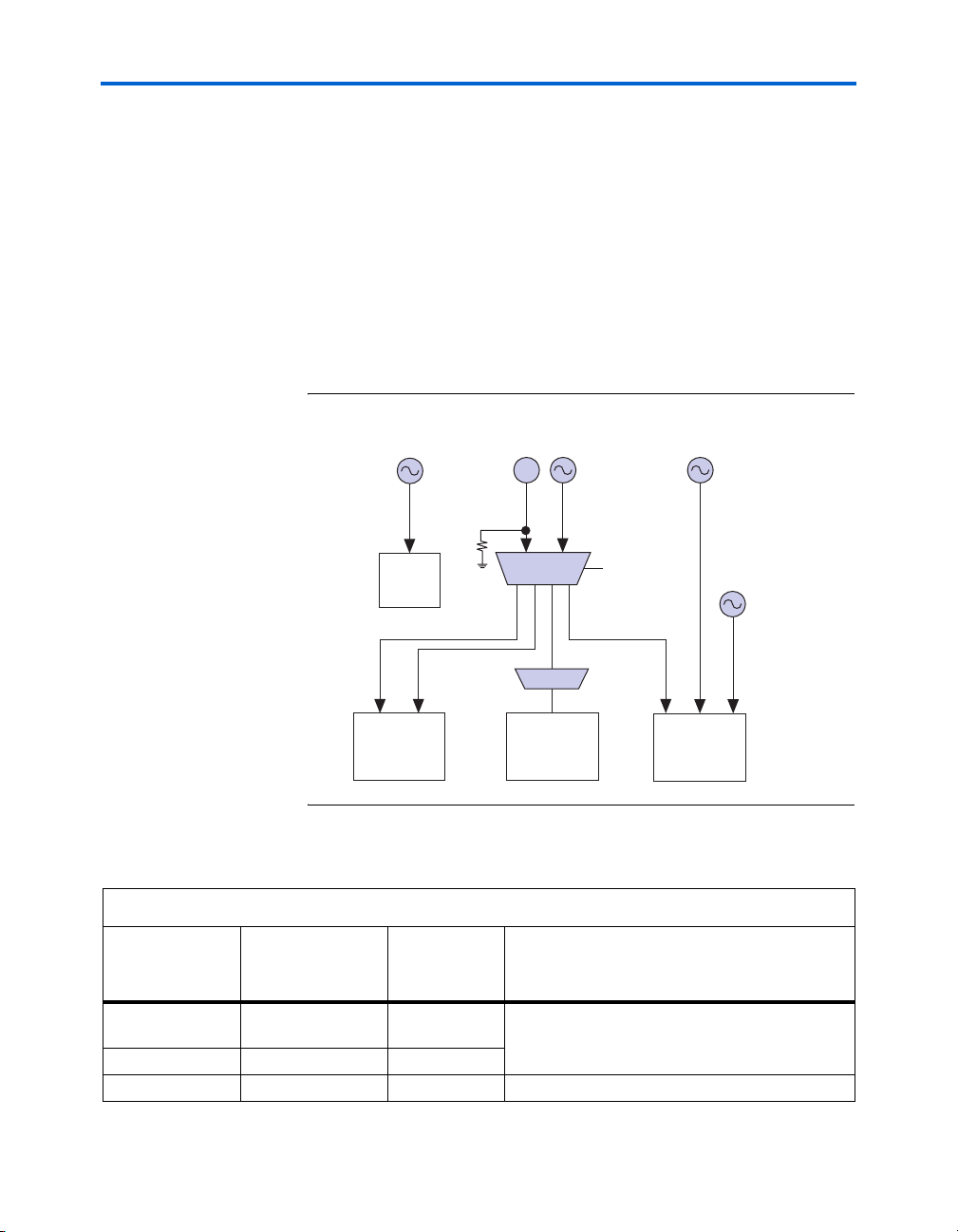
Clocking Circuitry
Three oscillators of 100 MHz, 156.25 MHz, and 155.52 MHz are used for
clocking the Stratix II GX transceivers and user logic. A fourth oscillator
of 25.000 MHz +/- 50 ppm is used as a reference clock for the Marvel
10/100/1000 Ethernet PHY device per manufacturing recommendations.
When the board is not plugged into a host board, the 100-MHz oscillator
is used to support the transceiver reference clock for PCIe applications.
Figure 2–6 shows the oscillator driving through a four-output LVDS
buffer to a variety of loads. The buffer can either be driven from the
100-MHz oscillator or from the SMA clock input for custom frequencies.
Pin 10 on the board configuration DIP switch controls what clock feeds
the buffer (see “Configuration DIP Switch (S6)” on page 2–23).
Figure 2–6. Oscillator Clocking Diagram
25 MHz
SMT OSC
LVTTL
88e1111
GigE
PHY
R
T
OSC A
SMA
LVTTL
Clock Buffer
LVDS
LVDS
LVDS
Translator
LVTTL
LVDS
100 MHz
SMT OSC
CLK_SEL
All A/C Coupled
OSC B
LVDS
156.250 MHz
SMT OSC
152.520 MHz
SMT OSC
LVDS
Stratix II GX
Enhanced PLL
Inputs
MAX II
Configuration
Controller
Stratix II GX
Enhanced PLL
Inputs
Table 2–4 lists the board’s clock distribution system.
Table 2–4. Stratix II GX PCIe Development Board Clock Distribution (Part 1 of 2)
Signal
Frequency Signal Name
Originates
Signal Propagates To
From
100 MHz 100M_OSC_P
100M_OSC_N
User input SMA clock input J4
25 MHz ENET_25M_CLK X2 Ethernet PHY
Altera Corporation Reference Manual 2–11
August 2006 Stratix II GX PCI Express Development Board
X1 U21 (ICS8543 clock buffer), Pins 4 and 5
Page 22

Configuration Schemes and Status LEDs
Table 2–4. Stratix II GX PCIe Development Board Clock Distribution (Part 2 of 2)
Signal
Frequency Signal Name
156.25 MHz xaui_refclk_cn X3 Stratix II GX pin H8 (REFCLK0_B13n)
xaui_refclk_cp Stratix II GX pin H7 (REFCLK0_B13p)
155.52 MHz SFP_REFCLK_P
SFP_REFCLK_N
Originates
From
X4 P: Stratix II GX pin P7 (RefClk0_B14P)
N: Stratix II GX pin P8 (RefClk0_P14N)
Signal Propagates To
Configuration
Schemes and
Status LEDs
f For information on the Quartus II Programmer, refer to Quartus II
The Stratix II GX device can be configured using two standard
configuration schemes, JTAG and Fast Passive Parallel (FPP). This section
discusses:
■ JTAG configuration
■ FPP configuration
■ Status and channel activity LEDs
JTAG Configuration
JTAG configuration is the simplest way to configure the Stratix II GX
device. The JTAG configuration scheme requires just the USB-Blaster
cable and the Quartus®II Software, Development Kit Edition (DKE),
which are both included with the kit.
For JTAG configuration setup, connect one end of the USB-Blaster cable
to the computer’s USB port and the other end to the 10-pin JTAG header
on the board. To download a design file to the Stratix II GX device, use the
Quartus II Programmer tool.
Development Software Handbook.
The board’s JTAG chain is connected to the Stratix II GX device, the
MAX II CPLD, and (optionally) the HSMC A and B expansion
connectors. To configure the Stratix II GX device, you need to:
™
■ Set up a new JTAG chain (including both the MAX II CPLD and the
Stratix II GX device)
■ Set the DIP switch (as noted in “Configuration DIP Switch (S6)” on
page 2–23) to remove the HSMC A and B expansion connectors from
the JTAG chain.
Figure 2–7 shows the JTAG chain connections.
2–12 Reference Manual Altera Corporation
Stratix II GX PCI Express Development Board August 2006
Page 23

Figure 2–7. JTAG Chain Connections
HSMC A
Board Components & Interfaces
3.3 V3.3 V
HSMC B
3.3 V
JTAG_TDI
JTAG Header
DIP Switch
HSMA_JTAG_TDO
DIP Switch
HSMA_JTAG_TDO
S2GX_JTAG_TDO
1.8 V
MAX II
CPLD
MAXII_JTAG_TDO
Because the Stratix II GX device’s TDO pin is located in a 1.8-V I/O bank,
the JTAG chain has a mixture of voltages. Table 2–5 shows the JTAG chain
signals based on the output.
Table 2–5. JTAG Chain I/O Signals
Signal Name Description Signal Type
JTAG_TCK JTAG clock (USB-Blaster output) 1.8 V CMOS
JTAG_TMS JTAG mode select (USB-Blaster output) 1.8 V CMOS
JTAG_TRST JTAG reset (USB-Blaster output) 1.8 V CMOS
JTAG_TDI Data output (USB-Blaster output) 1.8 V CMOS
HSMA_JTAG_TDO HSMC A data output (Bypassable at DIP switch) LVTTL
(Needs 3.3 V translation)
HSMB_JTAG_TDO HSMC B data output (Bypassable at DIP switch) LVTTL
(Needs 3.3 V translation)
MAXII_JTAG_TDO MAX II data output (Stratix II GX device input) 1.8 V CMOS
S2GX_JTAG_TDO Stratix II GX device data output (USB-Blaster input) 1.8 V CMOS
1.8 V
FPGA
f For more information about:
■ JTAG configuration, refer to Appendix A of the PCI Express
Development Kit, Stratix II GX Edition Getting Started User Guide.
■ Programming Altera devices, refer to the Configuration Handbook.
Altera Corporation Reference Manual 2–13
August 2006 Stratix II GX PCI Express Development Board
Page 24

Configuration Schemes and Status LEDs
FPP Configuration
Many applications involving PCIe require that a device being configured
enter the user operation mode before the computer containing the PCIe
card recognizes the PCIe bus. To facilitate this fast configuration scheme,
an on-board configuration controller is provided. The configuration
controller consists of a MAX II CPLD and a page-mode flash memory
device. When power is applied to the board, the MAX II CPLD loads a
configuration from the flash device into the Stratix II GX device in the
FPP mode. The MAX II CPLD holds the configuration state machine and
the flash memory holds the non-volatile configuration bit streams.
Figure 2–8 shows the FPP configuration scheme.
Figure 2–8. FPP Configuration Scheme
1.8V
100MHz
MAX II CPLD
MAX_EN
FPGA_nSTATUS
FPGA_nCONFIG
FPGA_CONF_DONE
FPGA_PGM[2:0]
FPGA_DATA[7:0]
FPGA_DCLK
LED
from DIPSW
1.8V1.8 V
10 kohm
Stratix II GX Device
INIT_DONE
n STAT U S
nCONFIG
CONF_DONE
nCE
RUnLU
PGM[2:0]
DATA[7:0]
DCLK
FLASH Interface
MSEL3
MSEL2
MSEL1
MSEL0
DIP Switch
RUnLU
CONFIG_MODE[1:0]
DIPSW+PGM[2:0]
FLASH_A[24:0]
FLASH_D[15:0]
FLASH_CEn
FLASH_OEn
FLASH_WEn
MSEL[3:0]
CFI FLASH
FLASH_A[25:0]
FLASH_D[15:0]
FLASH_CEn
FLASH_OEn
FLASH_WEn
FPGA_RSTn
FPGA_BYTEn
FPGA_RYBYn
10 kohm
1.8V
10 kohm
2–14 Reference Manual Altera Corporation
Stratix II GX PCI Express Development Board August 2006
Page 25

Board Components & Interfaces
f For information about board-supported FPGA configuration schemes,
refer to Table 2–7 on page 2–15.
Table 2–6 shows configuration file sizes for board-supported Stratix II GX
devices.
Table 2–6. Configuration File Sizes
Device
EP2SGX90 25,699,104 9,251,677
EP2SGX130 37,325,760 13,437,273
Notes to Ta b l e 2 –6 :
(1) This is a preliminary value based on both the EP2SGX90 and EP2SGX130 devices.
(2) This value assumes average reduction of 64%.
Configuration File Size
(Mb) (1)
Compressed File Size
(Mb) (2)
1 The 512-MB, on-board flash device is able to store either eight
designs of the EP2SGX90 device plus 32-Mbytes of additional
files, or eight designs of the EP2SGX130 device and 16-Mbytes of
additional files.
Table 2–7 shows the board-supported FPGA configuration schemes.
Table 2–7. Board-Supported FPGA Configuration Schemes & MSEL Settings
FPGA MSEL Settings (From MAX II CPLD) DIP Switch Settings
Configuration Scheme
MSEL-3 MSEL-2 MSEL-1 MSEL-0 Mode-1 Mode-0
Fast passive parallel (FPP) 0 0 0 0 0 0
Remote system upgrade
(RSU) FPP (1)
FPP with decompression 1 0 1 1 1 0
RSU FPP with
decompression (1)
JTAG N/A N/A N/A N/A N/A N/A
010001
110011
Note to Ta b le 2 – 7 :
(1) The RSU scheme uses the FPGA PGM(2:0) outputs page-select pins.
1 The same DIP switch used to select the configuration mode will
also have RUnLU pin control as well as some JTAG chain options.
Refer to the “General User Interfaces” on page 2–21 for more
information on the DIP switch.
Altera Corporation Reference Manual 2–15
August 2006 Stratix II GX PCI Express Development Board
Page 26

Configuration Schemes and Status LEDs
This section discusses:
■ Flash memory configuration file storage
■ MAX II configuration controller
Flash Memory Configuration File Storage
A 512-MB Spansion flash memory device is used to store configuration
files for the FPGA as well as any other necessary data. The target device
is a Spansion S29GL512N in a BGA package, which supports CFI flash
commands.
The flash memory map is determined by the MAX II CPLD design, which
is based on the parallel flash loader (PFL) megafunction. The PFL
megafunction takes up to eight Quartus II programmer object files (.pof)
and stacks them into a single image to be written to flash memory using
the Quartus II Programmer and a USB-Blaster cable. This is done via the
JTAG header and the MAX II CPLD to flash memory.
Table 2–8 lists an example flash memory map. The sizes of various blocks
may change based on the settings used, such as the compression setting,
in the Quartus II Programmer. The PFL Option Bits are used by the
MAX II CPLD design to store the address of the POF files. The Ethernet
Option Bits are used by MAC IP for IP and MAC address storage.
Table 2–8. Example Flash Memory Map (Part 1 of 2)
Memory Block Address
PFL Option Bits 0x03FF.FFFF
Ethernet Option Bits 0x03FF.FFEF
User Space
(16MB-32MB)
FPGA Design 7 0x01FF.FFFF
FPGA Design 6 0x01BF.FFFF
FPGA Design 5 0x017F.FFFF
FPGA Design 4 0x013F.FFFF
FPGA Design 3 0x00FF.FFFF
2–16 Reference Manual Altera Corporation
Stratix II GX PCI Express Development Board August 2006
0x03FF.FFF0
0x03FF.FFE0
0x03FF.FFDF
0x0200.0000
0x01C0.0000
0x0180.0000
0x0140.0000
0x0100.0000
0x00C0.0000
Page 27

Board Components & Interfaces
Table 2–8. Example Flash Memory Map (Part 2 of 2)
Memory Block Address
FPGA Design 2 0x00BF.FFFF
0x0080.0000
FPGA Design 1 0x007F.FFFF
0x0040.0000
FPGA Design 0 (default) 0x003F.FFFF
0x0000.0000
Table 2–9 lists the required signals for the flash memory. Signal directions
are relative to the FPGA as far as direction and signaling standard.
Table 2–9. Flash Interface I/O
Signal Name Description Signal Type
FLASH_A(24:0) Address bus 1.8-V CMOS out (25 bit)
FLASH_D(15:0) Data bus 1.8-V CMOS out (16 bit)
FLASH_CEn Chip enable 1.8-V CMOS out
FLASH_RESETn Reset 1.8-V CMOS out
FLASH_OEn Output enable 1.8-V CMOS out
FLASH_WEn Write enable 1.8-V CMOS out
FLASH_WPn Write protect N/A (Tie to VCC)
FLASH_RDYBSYn Ready/not busy 1.8-V CMOS in (Tie to VCC)
FLASH_BYTEn Byte/word select 1.8-V CMOS out (Tie to VCC)
VIO I/O power 1.8-V
VCC Core power 3.3-V
VSS Ground Ground
MAX II CPLD Configuration Controller
The MAX II CPLD is exclusively used for FPGA configuration and flash
programming. The target MAX II device is a 1.8 V-only EPM570GT100.
The PFL megafunction is the basis for the MAX II CPLD design.
When using the default PFL megafunction, k eep in mi nd t hat it ma y ne ed
to be modified to meet PCIe specification requirements. Specifically, the
PCIe specification states that a device be ready to enter the link training
state within 80 ms of the end of a fundamental reset (release of the
PERSTn pin). This can be a power-on-reset where the PWR GOOD signal is
Altera Corporation Reference Manual 2–17
August 2006 Stratix II GX PCI Express Development Board
Page 28

Configuration Schemes and Status LEDs
asserted within 100 ms of power levels being at the minimum level and
then an additional 100 ms for the reference clocks to stabilize. The
following text is an excerpt from the PCIe specification:
PCI Express Power-On-Reset Timing Specifications
The first set of rules addresses requirements for component devices:
■ A component must enter the initial active Link Training state within 80 ms
of the end of Fundamental Reset (Link Training is described in Section
4.2.4).
● Note: In some systems, it is possible that the two components on a Link
may exit Fundamental Reset at different times. Each component must
observe the requirement to enter the initial active Link Training state
within 80 ms of the end of Fundamental Reset from its own point of
view.
■ On the completion of Link Training (entering the DL_Active state, see
Section 3.2), a component must be able to receive and process TLPs and
DLLps.
The second set of rules addresses requirements placed on the system:
■ To allow components to perform internal initialization, system software
must wait for at least 100 ms from the end of a reset of one or more devices
before it is permitted to issue Configuration Requests to those devices.
● A system must guarantee that all components intended to be software
visible at boot time are ready to receive Configuration Requests within
100 ms of the end of Fundamental Reset at Root Complex - how this is
done is beyond the scope of this specification.
The MAX II CPLD is part of the board’s JTAG chain and can be
programmed using the Quartus II Programmer and a USB-Blaster cable.
The same JTAG interface is also used to program flash images.
Table 2–10 lists the required MAX II CPLD signals and the corresponding
PFL megafunction design I/O requirements. Signal directions are relative
to the CPLD as far as direction and signaling standard.
Table 2–10. MAX II CPLD Signals & I/O Requirements (Part 1 of 2)
Signal Name Description Signal Type
FPGA_CONFIG_DCLK Configuration clock 1.8-V CMOS out
FPGA_CONFIG_D(7:0) Configuration data bus 1.8-V CMOS out (8 bits)
CONF_DONE FPGA CONF_DONE pin
connection
2–18 Reference Manual Altera Corporation
Stratix II GX PCI Express Development Board August 2006
1.8-V CMOS in
Page 29

Board Components & Interfaces
Table 2–10. MAX II CPLD Signals & I/O Requirements (Part 2 of 2)
Signal Name Description Signal Type
CONFIGn FPGA nCONFIG pin
connection
STATUSn FPGA nSTATUS pin
connection
FLASH_A(24:0) Flash address bus 1.8-V CMOS out (25 bit)
FLASH_D Flash data bus 1.8 -V CMOS in/out (16 bit)
FLASH_CEn Flash chip enable 1.8-V CMOS out
FLASH_OEn Flash output enable 1.8-V CMOS out
FLASH_WEn Flash write enable 1.8-V CMOS out
CONFIG_MODE(1:0) Configuration mode input 1.8-V CMOS in (2 bits)
MSEL(3:0) FPGA mode select output 1.8-V CMOS out (4 bits)
MAX_EN Enables operation for
PFL
FPGA_PGM(2:0) Remote configuration
page select
DIPSW_PGM(2:0) DIP switch configuration
page select
MAXII_CLK_IN 100-MHz clock input 1.8-V CMOS in
TMS JTAG mode select N/A
TDI JTAG data in N/A
TDO JTAG data out N/A
TCK JTAG clock N/A
VCCIO1 I/O bank 1 power 1.8 V
VCCIO2 I/O bank 2 power 1.8 V
VCCINT Core power 1.8 V
GNDIO I/O GND GND
GNDINT Core GND GND
1.8-V CMOS in
1.8-V CMOS in
1.8-V CMOS in
1.8-V CMOS in (3 bits)
1.8-V CMOS in (3 bits)
1 For more information about the advanced parallel flash loader
settings, refer to Chapter 2 of the Configuration Handbook,
Configuring Stratix II and Stratix II GX Devices.
Altera Corporation Reference Manual 2–19
August 2006 Stratix II GX PCI Express Development Board
Page 30

Configuration Schemes and Status LEDs
Status and Channel Activity LEDs
The board provides status and channel activity LEDs, which indicate
successful configuration, power-on status, connection to expansion
connectors, etc. Tables 2–11 and 2–12 list board status and channel activity
LEDs.
Table 2–11. Status LEDs
Board Reference Number Indicates
D1 HSMC A detected
D2 HSMC B detected
D8 Successful configuration
D19 Power-on
D20 Gigabit Ethernet 10 Mb link
D21 Gigabit Ethernet 100 Mb link
D22 Gigabit Ethernet 1000 Mb link
Table 2–12. Channel Activity LEDs
Board Reference Number Indicates
D3 HSMC A TX
D4 HSMC A RX
D5 HSMC B TX
D6 HSMC B RX
D17 Ethernet RX
D18 Ethernet TX
D23 SFP A RX
D24 SFP A TX
D25 SFP B RX
D26 SFP B TX
D27 PCI Express x1
D28 PCI Express x2
D29 PCI Express x3
2–20 Reference Manual Altera Corporation
Stratix II GX PCI Express Development Board August 2006
Page 31

Board Components & Interfaces
General User Interfaces
To allow you to fully leverage the I/O capabilities of the Stratix II GX
device for debugging, control, and monitoring purposes, the following
general user interfaces are available on the board:
■ Push buttons
■ User DIP switch
■ User LEDs
■ Board-specific DIP switch
■ Board-specific LEDs
Push Button Switches (S1 Through S4)
Board references S1 through S4 are push-button switches allowing
general user I/O interfaces to the Stratix II GX device.
The nCONFIG push button has a direct connection to the Stratix II GX
device’s nCONFIG signal that—upon pressing to drive low—forces an
erase and reprogram of the FPGA’s design. The other push buttons
connect directly to user I/O pins for user programming. Although the
RESET push button’s purpose is programming, its special label is
intended to encourage its use as a logic reset signal for FPGA designs so
that user designs are reset in a consistent manner.
Table 2–13 lists the schematic signal names and corresponding
Stratix II GX pin numbers.
Table 2–13. Push-Button Switch Signal Names and Functions
Board Reference
S1 nCONFIG N/A
S2 USER_PB1 D37
S3 USER_PB0 E36
S4 USER_RESET AM22
Schematic
Signal Name
Stratix II GX Pin Number
1 Board reference S1 is tied to the nCONFIG signal on the Stratix II
GX device. Pushing the S1 switch causes the FPGA to reload a
configuration from the on-board flash device. Pin AM22 is the
DEV_CLRn pin; when enabled in the Quartus II software, it will
reset all Stratix II GX device registers. Pin AM22 can also be used
as a standard input.
Altera Corporation Reference Manual 2–21
August 2006 Stratix II GX PCI Express Development Board
Page 32

General User Interfaces
User-Defined DIP Switch (S5)
Board reference S5 is an eight-pin DIP switch. The DIP switches in S5 are
user-defined, and are provided for additional FPGA input control. Each
pin can be set to a logic 1 by pushing it to the open position, and each pin
can be set to logic 0 by pushing it to the closed position.
Table 2–14 lists the DIP switch settings, schematic signal name, and
corresponding Stratix II GX device’s pin number.
Table 2–14. User-Defined DIP Switch Pin-Out (S5)
S5 Switch Schematic Signal Name Stratix II GX Device Pin
1 USER_DIPSW0 V36
2 USER_DIPSW1 V34
3 USER_DIPSW2 V35
4 USER_DIPSW3 W33
5 USER_DIPSW4 V33
6 USER_DIPSW5 W34
7 USER_DIPSW6 V32
8 USER_DIPSW7 V27
Figure 2–9 shows the user-defined DIP switch board image.
Figure 2–9. User-Defined DIP Switch Board Image
2–22 Reference Manual Altera Corporation
Stratix II GX PCI Express Development Board August 2006
Page 33

Board Components & Interfaces
User LEDs (D9 Through D16)
The board provides eight user-defined LEDs. A logic 0 driven to an LED
turns it off; a logic 1 driven to an LED turns it on.
Table 2–15 lists the schematic signal name and the corresponding
Stratix II GX device’s pin number.
Table 2–15. User-Defined LED Pin-Out
Board Reference Schematic Signal Name
D9 USER_LED0 AR33
D10 USER_LED1 AP30
D11 USER_LED2 AT32
D12 USER_LED3 AP31
D13 USER_LED4 AU34
D14 USER_LED5 AT33
D15 USER_LED6 AN31
D16 USER_LED7 AT31
Stratix II GX Device
Pin Number
Configuration DIP Switch (S6)
The configuration DIP switch is used to set up specific board functions,
such as FPGA bootstrap settings, JTAG chain bypassing, or configuration
setup. In the open position, the selected signal is driven to logic 0. In the
closed position, the selected signal is driven to a logic 1.
Altera Corporation Reference Manual 2–23
August 2006 Stratix II GX PCI Express Development Board
Page 34

General User Interfaces
Table 2–16 shows the configuration DIP switch (S6) signal names and
descriptions.
Table 2–16. Configuration DIP Switch (S6) Signal Names and Descriptions
Schematic Signal Name Description
CONFIG_MODE0 Configuration mode - bit 0
CONFIG_MODE1 Configuration mode - bit 1
DIPSW_PGM0 Configuration file page select - bit 0
DIPSW_PGM1 Configuration file page select - bit 1
DIPSW_PGM2 Configuration file page select - bit 2
VCCHTX_ADJ Transceiver power select (on = 1.5 V, off = 1.2 V)
RUnLU Remote/local configuration mode
HSMCA_JTAG HSMC-A JTAG bypass (close to bypass HSMC-A)
HSMCB_JTAG HSMC-B JTAG bypass (close to bypass HSMC-B)
CLK_SEL Local oscillator / SMA input select (on = local
oscillator)
Board-Specific LEDs
This section describes the two types of board-specific LEDs:
■ FPGA transceiver channel activity LEDs
■ Power, configuration, and traffic activity LEDs
FPGA Transceiver Channel Activity LEDs
In addition to the user-defined LEDs, the board provides a set of 12
yellow LEDs (2 per interface). These board-specified LEDs are used to
display FPGA transceiver channel activity (or traffic) on a XCVR interface
basis for both TX and RX signals.
Table 2–17 shows the channels needing TX and RX LEDs.
Table 2–17. FPGA Transceiver Interface LEDs (Part 1 of 2)
Number Transceiver Interface Indicator LED Color
1 PCIe edge connector (L0x1, L0x4, L0x8) Yellow
2 SFP A interface (TX & RX) Yellow
3 SFP B interface (TX & RX) Yellow
4 Gigabit Ethernet (TX & RX) Yellow
2–24 Reference Manual Altera Corporation
Stratix II GX PCI Express Development Board August 2006
Page 35

Board Components & Interfaces
Table 2–17. FPGA Transceiver Interface LEDs (Part 2 of 2)
Number Transceiver Interface Indicator LED Color
5 HSMC A interface (TX & RX) Yellow
6 HSMC B interface (TX & RX) Yellow
Power, Configuration, and Traffic Activity LEDs
The board provides many other special purpose LEDs. For example, a set
of display power status (PWR_ON when illuminated) LEDs as well as
FPGA configuration status LEDs (LED_ON if the FPGA is programmed).
Additionally, two other LEDs are provided to display traffic activity as
well as link status on GigE on the RJ-45 jack. Table 2–18 shows the
transceiver interface and LED colors.
Table 2–18. Power, Configuration, and Traffic Activity LEDs
Standard Communication Ports
Number
1 GigE – 10 Mb link Green
2 GigE – 100 Mb link Green
4 GigE – 1000 Mb link Green
5 HSMC-A present Green
6 HSMC-B present Green
7 CONF_DONE Green
8 PWR_ON Blue
The board supports the following communication ports discussed in this
section:
■ PCIe edge connector interface
■ Gigabit Ethernet interface
■ SFP module interface
■ High-speed Mezzazine card interfaces (A and B)
■ JTAG interface
Transceiver Interface
Indicators
LED Color
PCI Express Edge Connector Interface (J9)
The board features a x8 PCIe edge connector. The high speed PCIe signals
are directly routed to two Stratix II GX device transceivers quads. The
PCIe signals have 100 differential traces terminated on the receive-side
Altera Corporation Reference Manual 2–25
August 2006 Stratix II GX PCI Express Development Board
Page 36

Standard Communication Ports
using internal termination resistors in the Stratix II GX device receiver
pins. Table 2–19 lists the PCIe edge connector pin-out and corresponding
Stratix II GX device pin number..
pcie_led_x1 AU11
pcie_led_x4 AG16
pcie_led_x8 AM13
pcie_perstn AL16
pcie_refclk_n AB8
pcie_refclk_p AB7
pcie_rx_n[0] AG2
pcie_rx_n[1] AE2
pcie_rx_n[2] AJ2
pcie_rx_n[3] AL2
pcie_rx_n[4] W2
pcie_rx_n[5] U2
pcie_rx_n[6] AA2
pcie_rx_n[7] AC2
pcie_rx_p[0] AG1
pcie_rx_p[1] AE1
pcie_rx_p[2] AJ1
pcie_rx_p[3] AL1
pcie_rx_p[4] W1
pcie_rx_p[5] U1
pcie_rx_p[6] AA1
pcie_rx_p[7] AC1
pcie_smbclk AK18
pcie_smbdat AH20
pcie_tx_n[0] AG5
pcie_tx_n[1] AE5
pcie_tx_n[2] AJ5
pcie_tx_n[3] AL5
pcie_tx_n[4] W5
pcie_tx_n[5] U5
pcie_tx_n[6] AA5
Table 2–19. PCIe Edge Connector Pin-Out
Schematic Signal Name Stratix II GX Pin Number
2–26 Reference Manual Altera Corporation
Stratix II GX PCI Express Development Board August 2006
Page 37

Board Components & Interfaces
Table 2–19. PCIe Edge Connector Pin-Out
Schematic Signal Name Stratix II GX Pin Number
pcie_tx_n[7] AC5
pcie_tx_p[0] AG4
pcie_tx_p[1] AE4
pcie_tx_p[2] AJ4
pcie_tx_p[3] AL4
pcie_tx_p[4] W4
pcie_tx_p[5] U4
pcie_tx_p[6] AA4
pcie_tx_p[7] AC4
pcie_waken AT10
The PCIe specification allows for a maximum of 25 W of add-in card
power dissipation. If a card must be over 25 W, then it must power-up in
a state of 25 W or less and wait for the server to register the card as a
high-power device. The card can then ramp up to a maximum of no more
than 40-W total power dissipation.
The x8 edge connector provides 12-V @ 2.1A (max) and 3.3-V @ 3A (max).
There is also a 3.3-V AUX provided for up to 375 mA for wake-on-LAN
and other power sequencing circuitry.
1 These numbers are valid for typical servers or workstations.
They are not valid for stand-alone operation outside of a host
board where all power is derived from an external DC input
jack.
The REFCLKp and REFCLKn signals are the 100-MHz (±300 PPM)
differential reference clock that is driven from a base-board onto the PCIe
add-in card. This is used as the reference clock for the FPGA transceivers
connected to the HSIO data channels. The nominal swing for each
single-ended signal of the differential pair is from 0 V to 700 mV.
The I/O standard is called high-speed current steering logic (HCSL),
which Figure 2–10 shows along with the Voh/Vol levels that should be
expected as inputs to the card. The clocks are terminated on the host and
should DC couple to the Stratix II GX FPGA.
Altera Corporation Reference Manual 2–27
August 2006 Stratix II GX PCI Express Development Board
Page 38

Standard Communication Ports
Figure 2–10. PCI Express Reference Clock Levels
VOH = 0.525V
V
CROSS
VOL = 0.175V
Gigabit Ethernet (GigE) Interface (RJ1)
The board’s GigE interface is implemented with an RJ-45 jack and a
dedicated 10/100/1000 base-T, auto-negotiating Ethernet physical
device. The media access controller (MAC) layer must be implemented in
the FPGA and connect to the PHY device through either the Gigabit
medium independent interface (GMII) or medium independent interface
(MII).
Clock#
T
T
FALL
(Clock)
RISE
(Clock#)
Clock
Figure 2–11 shows the interface between the Stratix II GX device’s MAC
and the GigE PHY layer.
2–28 Reference Manual Altera Corporation
Stratix II GX PCI Express Development Board August 2006
Page 39

Board Components & Interfaces
Figure 2–11. Marvell 88E1111 GigE PHY Layer & GMII Interface to the FPGA
GMII Interface
Stratix II GX
MAC Block
GTX_CLK
TX_ER
TX_EN
TXD[7:0]
RX_CLK
RX_ER
RX_DV
RXD[7:0]
CRS
COL
GTX_CLK
TX_ER
TX_EN
TXD[7:0]
RX_CLK
RX_ER
RX_DV
RXD[7:0]
CRS
COL
Marvell 88E1111
GigE PHY Layer
f For more information about the Stratix II GX Gigabit Ethernet MAC
megafunction, please refer to the following:
■ Stratix II GX Embedded Ethernet MAC/PHY Users Guide (Verilog HDL)
■ Stratix II GX Embedded Ethernet MAC/PHY Users Guide (VHDL)
■ Stratix II GX Handbook
Table 2–20 lists the RJ-45 jack board reference and description.
Table 2–20. Component Reference RJ-45 Jack
Board Reference Device Description
RJ1 RJ-45 single-port jack
Table 2–21 lists manufacturing information.
Table 2–21. Manufacturing Information
Manufacturer
HALO Electronics HFJ11-1G02E www.haloelectronics.com
Altera Corporation Reference Manual 2–29
August 2006 Stratix II GX PCI Express Development Board
Manufacturer Part
Number
Manufacturer Website
Page 40

Standard Communication Ports
Table 2–22 lists GigE PHY layer component reference information.
Table 2–22. Component Reference GigE PHY Layer
Board
Reference
U1 10/100/1000 GigE PHY Marvel Electronics 88E1111 www.marvell.com
Device Description Manufacturer
Manufacturer Part
Number
Manufacturer
Website
Table 2–23 lists GigE PHY pin-out and corresponding Stratix II GX device
pin numbers.
Table 2–23. GigE PHY Pin-Out (Part 1 of 2)
Schematic Signal Name Stratix II GX Device Pin Number
enet_col C26
enet_crs D31
enet_gtx_clk B33
enet_intn A29
enet_mdc A28
enet_mdio E34
enet_resetn H31
enet_rx_clk M27
enet_rx_dv E28
enet_rx_er G24
enet_rxd[0] G28
enet_rxd[1] A35
enet_rxd[2] D23
enet_rxd[3] C28
enet_rxd[4] B24
enet_rxd[5] F25
enet_rxd[6] C32
enet_rxd[7] G26
enet_tx_clk F28
enet_tx_en A37
enet_tx_er P22
enet_txd[0] N24
enet_txd[1] J27
enet_txd[2] C24
2–30 Reference Manual Altera Corporation
Stratix II GX PCI Express Development Board August 2006
Page 41

Board Components & Interfaces
Table 2–23. GigE PHY Pin-Out (Part 2 of 2)
Schematic Signal Name Stratix II GX Device Pin Number
enet_txd[3] C29
enet_txd[4] D26
enet_txd[5] J30
enet_txd[6] F26
enet_txd[7] F21
The interface to the GigE PHY layer can also use the MII interface for 10
and 100 Mb/s signaling. Table 2–24 shows the GMII-to-MII interface
mapping.
Table 2–24. GMII-to-MII I/O Mapping, Note (1)
Marvel Target
Device Pins
GTX_CLK GTX_CLK —
TX_CLK — TX_CLK
TX_ER TX_ER TX_ER
TX_EN TX_EN TX_EN
TXD[7:0] TXD[7:0] TXD[3:0]
RX_CLK RX_CLK RX_CLK
RX_ER RX_ER RX_ER
RX_DV RX_DV RX_DV
RXD[7:0] RXD[7:0] RXD[3:0]
CRS CRS CRS
COL COL COL
Note to Table 2–24:
(1) The 1.8-V logic outputs on the FPGA are up-converted using an FXL4T245
dual-voltage buffer. The 2-5-V CMOS outputs from the Marvel 88E1111 device are
over-driving the FPGA input pins.
GMII Interface Standard MII Interface Standard
The GMII interface is single-data-rate (SDR), source-synchronous in
nature, and operates at 125 MHz. Whereas, the reduced gigabit media
independent interface (RGMII) uses half of the eight data pins, but also
operates at 125 MHz. The RGMII interface achieves the 50% pin count
reduction by using DDR flip flops. The Stratix II GX PCIe development
board can use either the GMII or RGMII interface. However, because of
it’s simpler timing model, the GMII interface is preferred.
Altera Corporation Reference Manual 2–31
August 2006 Stratix II GX PCI Express Development Board
Page 42

Standard Communication Ports
Because the GMII interface bank’s voltage level for the FPGA is only
1.8 V, voltage translators are required to “up-convert” the 1.8 V FPGA
outputs using FXL4T245 dual-voltage buffers. The 2.5-V CMOS outputs
from the Marvell 88E1111 are over-driving the FPGA input pins (2.5 V
CMOS driving 1.8 V buffer inputs). The source-synchronous timing is
affected by this up-conversion as the buffers have their own pin-to-pin
delay specification.
Figure 2–12 shows the source-synchronous GMII interface TX timing
diagram.
Figure 2–12. Marvell 88E1111 GMII TX Timing Diagram
T
P_GMII_GTX_CLK
T
R_GMII_GTX_CLK
GTX_CLK
T
H_GMII_GTX_CLK
T
F_GMII_GTX_CLK
T
R_GMII_GTX_CLK
V
V
IH_GMII
IL_GMII
(Min.)
(Max.)
TDX[7:0]
TX_EN
TX_ER
(Min.)
V
IH_GMII
(Max.)
V
IL_GMII
T
SU_GMII_GTX_CLK
T
HD_GMII_GTX_CLK
The board provides an internal MAC core as an application layer
interface for user designs. You can test it by accessing the stack provided
as an Altera SOPC Builder component.
An IP core is also available from the Altera Megafunctions Partner
SM
Program (AMPP
) partner MorethanIP. The MorethanIP core has been
used and tested on an existing Altera daughter card using the Nios II
processor core and the MorethanIP TCP/IP driver software for the Nios II
processor.
1 Additional GigE ports can be added using plug-in modules on
the board’s SFP connectors for either copper or optical
applications.
2–32 Reference Manual Altera Corporation
Stratix II GX PCI Express Development Board August 2006
Page 43

Board Components & Interfaces
SFP A and B Interfaces (J6 and J7)
Two SFP standard cages (SFP_A and SFP_B) connect to the Stratix II GX
device’s transceivers and protrude through the PCIe panel. These two
interfaces are designed per the SFP MSA specifications. Modules that
comply with the SFP MSA specifications include networking standards,
such as asynchronous transfer mode (ATM), fiber distributed data
interface (FDDI), Fiber Channel, and GigE (both copper and optical).
The SFP MSA requires signals only up to 5.0 Gb/s, but standard modules
available today are typically 2.488 Gb/s synchronous optical net
(SONET) mode or below. The board is designed to deliver electrical
transceiver signals up to 5.0 Gb/s to each SFP connector. The two
channels of transceivers dedicated from the FPGA come from the same
transceiver block as two of the channels that are routed to the HSMC-A
transceiver interface. See “High-Speed Mezzanine Connectors A and B
Interface” on page 2–35.
Figure 2–13 shows an SFP pin-out diagram.
Figure 2–13. SFP Pin-Out Diagram
SFP Module
Towards Bezel
120
2 TXFault
3 TXDisable
4 MOD-DEF(2)
5
6 MOD-DEF(0)
7 Rate Select
8 LOS
9V
10 VeeR
MOD-DEF(1)
R
ee
VeeT
TD-
TD+
VeeT
VccT
VccR
VeeR
RD+
RD-
VeeR
20
19
18
17
Towards FPGA
16
15
14
13
12
11
Altera Corporation Reference Manual 2–33
August 2006 Stratix II GX PCI Express Development Board
Page 44

Standard Communication Ports
Table 2–25 lists the SFP A and B pin-out and corresponding Stratix II GX
pin number.
sfp_refclk_cn P8
sfp_refclk_cp P7
sfpa_led_rx L16
sfpa_led_tx K15
sfpa_los H16
sfpa_mod0_prsntn D11
sfpa_mod1_scl N15
sfpa_mod2_sda G11
sfpa_ratesel J21
sfpa_rx_n0 N2
sfpa_rx_p0 N1
sfpa_tx_n0 N5
sfpa_tx_p0 N4
sfpa_txdisable F10
sfpa_txfault C9
sfpb_led_rx L15
sfpb_led_tx H18
sfpb_los M16
sfpb_mod0_prsntn P18
sfpb_mod1_scl N18
sfpb_mod2_sda N17
sfpb_ratesel K18
sfpb_rx_n0 R2
sfpb_rx_p0 R1
sfpb_tx_n0 R5
sfpb_tx_p0 R4
sfpb_txdisable C12
sfpb_txfault J18
Table 2–25. SFP A and B Pin-Out
Schematic Signal Name Stratix II GX Pin Number
2–34 Reference Manual Altera Corporation
Stratix II GX PCI Express Development Board August 2006
Page 45

Board Components & Interfaces
High-Speed Mezzanine Connectors A and B Interface
The high-speed Mezzanine connector (HSMC) is an Altera-developed
specification, which allows users to expand the functionality of the PCIe
development board through the addition of daughter cards (HSMC
cards).
The specification allows for eight transceiver channels, up to 18 LVDS
channels (plus differential clock input and output), 6 single ended I/O
(plus dedicated clock input and output), a JTAG bus, 3.3 V, 12 volts, and
GND.
f For more information about the Altera HSMC connectors, refer to the
HSMC specifications on the Altera website, www.altera.com.
The Stratix II GX device has 16 transceivers: Two are used by the SFP
connectors and eight are used by the PCIe edge connector, which leaves
only six for the HSMC connectors. Therefore, HSMC A has only four
transceivers routed to it and HSMC B has only two transceivers routed to
it. This is the only deviation from the HSMC specification made on these
connectors.
Table 2–26 lists the HSMC A and B connector component reference and
manufacturing information.
Table 2–26. HSMC A and B Connectors
Board
Reference
J1, J2 High speed Mezzanine
connector
Description Manufacturer
Samtec ASP-122953-01 www.samtec.com
Manufacturer Part
Number
Manufacturer
Website
Table 2–27 lists HSMC A connector pin-out as well as corresponding
Samtec and Stratix II GX pin numbers.
Table 2–27. HSMC A Connector Pin-Out (Part 1 of 5)
Schematic Signal Name Samtec Pin Number Stratix II GX Pin Number
hsma_clk_in_n1 98 C38
hsma_clk_in_n2 158 V38
hsma_clk_in_p1 96 C39
hsma_clk_in_p2 156 V39
hsma_clk_in0 40 V37
hsma_clk_out_n1 97 Y31
Altera Corporation Reference Manual 2–35
August 2006 Stratix II GX PCI Express Development Board
Page 46

Standard Communication Ports
hsma_clk_out_n2 157 T30
hsma_clk_out_p1 95 W32
hsma_clk_out_p2 155 T31
hsma_clk_out0 39 G22
hsma_d[0] 41 D22
hsma_d[1] 42 F22
hsma_d[2] 43 A22
hsma_d[3] 44 B22
hsma_led_rx N/A B31
hsma_led_tx N/A F29
hsma_rx_d_n[0] 50 J38
hsma_rx_d_n[1] 56 K37
hsma_rx_d_n[10] 116 L39
hsma_rx_d_n[11] 122 R36
hsma_rx_d_n[12] 128 M38
hsma_rx_d_n[13] 134 P39
hsma_rx_d_n[14] 140 T34
hsma_rx_d_n[15] 146 R38
hsma_rx_d_n[16] 152 T39
hsma_rx_d_n[2] 62 L36
hsma_rx_d_n[3] 68 M36
hsma_rx_d_n[4] 74 N37
hsma_rx_d_n[5] 80 P36
hsma_rx_d_n[6] 86 R34
hsma_rx_d_n[7] 92 T37
hsma_rx_d_n[8] 104 U36
hsma_rx_d_n[9] 110 N35
hsma_rx_d_p[0] 48 J39
hsma_rx_d_p[1] 54 K38
hsma_rx_d_p[10] 114 K39
hsma_rx_d_p[11] 120 R37
hsma_rx_d_p[12] 126 M39
hsma_rx_d_p[13] 132 N39
hsma_rx_d_p[14] 138 T35
Table 2–27. HSMC A Connector Pin-Out (Part 2 of 5)
Schematic Signal Name Samtec Pin Number Stratix II GX Pin Number
2–36 Reference Manual Altera Corporation
Stratix II GX PCI Express Development Board August 2006
Page 47

Board Components & Interfaces
Table 2–27. HSMC A Connector Pin-Out (Part 3 of 5)
Schematic Signal Name Samtec Pin Number Stratix II GX Pin Number
hsma_rx_d_p[15] 144 R39
hsma_rx_d_p[16] 150 U39
hsma_rx_d_p[2] 60 L37
hsma_rx_d_p[3] 66 M37
hsma_rx_d_p[4] 72 N38
hsma_rx_d_p[5] 78 P37
hsma_rx_d_p[6] 84 R35
hsma_rx_d_p[7] 90 T38
hsma_rx_d_p[8] 102 U37
hsma_rx_d_p[9] 108 N36
hsma_rx_n[0] 32 C2
hsma_rx_n[1] 28 A4
hsma_rx_n[2] 24 E2
hsma_rx_n[3] 20 G2
hsma_rx_n[4] 16 J2
hsma_rx_n[5] 12 L2
hsma_rx_p[0] 30 C1
hsma_rx_p[1] 26 A3
hsma_rx_p[2] 22 E1
hsma_rx_p[3] 18 G1
hsma_rx_p[4] 14 J1
hsma_rx_p[5] 10 L1
hsma_scl 34 H36
hsma_sda 33 F38
hsma_tx_d_n[0] 49 G32
hsma_tx_d_n[1] 55 J31
hsma_tx_d_n[10] 115 L33
hsma_tx_d_n[11] 121 R27
hsma_tx_d_n[12] 127 N33
hsma_tx_d_n[13] 133 P33
hsma_tx_d_n[14] 139 R32
hsma_tx_d_n[15] 145 T32
hsma_tx_d_n[16] 151 U33
hsma_tx_d_n[2] 61 K31
hsma_tx_d_n[3] 67 L31
Altera Corporation Reference Manual 2–37
August 2006 Stratix II GX PCI Express Development Board
Page 48

Standard Communication Ports
hsma_tx_d_n[4] 73 M31
hsma_tx_d_n[5] 79 N31
hsma_tx_d_n[6] 85 R31
hsma_tx_d_n[7] 91 T29
hsma_tx_d_n[8] 103 P28
hsma_tx_d_n[9] 109 K33
hsma_tx_d_p[0] 47 G33
hsma_tx_d_p[1] 53 J32
hsma_tx_d_p[10] 113 L34
hsma_tx_d_p[11] 119 P27
hsma_tx_d_p[12] 125 N34
hsma_tx_d_p[13] 131 P34
hsma_tx_d_p[14] 137 R33
hsma_tx_d_p[15] 143 T33
hsma_tx_d_p[16] 149 U34
hsma_tx_d_p[2] 59 K32
hsma_tx_d_p[3] 65 K30
hsma_tx_d_p[4] 71 M32
hsma_tx_d_p[5] 77 N32
hsma_tx_d_p[6] 83 P30
hsma_tx_d_p[7] 89 R30
hsma_tx_d_p[8] 101 N27
hsma_tx_d_p[9] 107 K34
hsma_tx_n[0] 31 C5
hsma_tx_n[1] 27 A7
hsma_tx_n[2] 23 E5
hsma_tx_n[3] 19 G5
hsma_tx_n[4] 15 J5
hsma_tx_n[5] 11 L5
hsma_tx_p[0] 29 C4
hsma_tx_p[1] 25 A6
hsma_tx_p[2] 21 E4
hsma_tx_p[3] 17 G4
Table 2–27. HSMC A Connector Pin-Out (Part 4 of 5)
Schematic Signal Name Samtec Pin Number Stratix II GX Pin Number
2–38 Reference Manual Altera Corporation
Stratix II GX PCI Express Development Board August 2006
Page 49

Board Components & Interfaces
Table 2–27. HSMC A Connector Pin-Out (Part 5 of 5)
Schematic Signal Name Samtec Pin Number Stratix II GX Pin Number
hsma_tx_p[4] 13 J4
hsma_tx_p[5] 9 L4
Table 2–28 lists HSMC B connector pin-out as well as cooresponding
Samtec and Stratix II GX pin numbers.
Table 2–28. HSMC B Connector Pin-Out
Schematic Signal Name Samtec Pin Number
hsmb_clk_in_n1 98 W38
hsmb_clk_in_n2 158 AU38
hsmb_clk_in_p1 96 W39
hsmb_clk_in_p2 156 AU39
hsmb_clk_in0 40 W37
hsmb_clk_out_n1 97 AM33
hsmb_clk_out_n2 157 AE31
hsmb_clk_out_p1 95 AM34
hsmb_clk_out_p2 155 AE32
hsmb_clk_out0 39 AN22
hsmb_d[0] 41 AR22
hsmb_d[1] 42 AT22
hsmb_d[2] 43 AT21
hsmb_d[3] 44 AP22
hsmb_led_rx N/A AF25
hsmb_led_tx N/A AV33
hsmb_rx_d_n[0] 50 _AE36
hsmb_rx_d_n[1] 56 AE38
hsmb_rx_d_n[10] 116 AG35
hsmb_rx_d_n[11] 122 AH36
hsmb_rx_d_n[12] 128 AJ36
hsmb_rx_d_n[13] 134 AK35
hsmb_rx_d_n[14] 140 AL38
hsmb_rx_d_n[15] 146 AP38
hsmb_rx_d_n[16] 152 AT39
hsmb_rx_d_n[2] 62 AG39
Stratix II GX
Pin Number
Altera Corporation Reference Manual 2–39
August 2006 Stratix II GX PCI Express Development Board
Page 50

Standard Communication Ports
Table 2–28. HSMC B Connector Pin-Out
Schematic Signal Name Samtec Pin Number
hsmb_rx_d_n[3] 68 AG37
hsmb_rx_d_n[4] 74 AH38
hsmb_rx_d_n[5] 80 AK39
hsmb_rx_d_n[6] 86 AK37
hsmb_rx_d_n[7] 92 AM39
hsmb_rx_d_n[8] 104 AE34
hsmb_rx_d_n[9] 110 AF36
hsmb_rx_d_p[0] 48 AE37
hsmb_rx_d_p[1] 54 AE39
hsmb_rx_d_p[10] 114 AG36
hsmb_rx_d_p[11] 120 AH37
hsmb_rx_d_p[12] 126 AJ37
hsmb_rx_d_p[13] 132 AK36
hsmb_rx_d_p[14] 138 AL39
hsmb_rx_d_p[15] 144 AP39
hsmb_rx_d_p[16] 150 AR39
hsmb_rx_d_p[2] 60 AF39
hsmb_rx_d_p[3] 66 AG38
hsmb_rx_d_p[4] 72 AH39
hsmb_rx_d_p[5] 78 AJ39
hsmb_rx_d_p[6] 84 AK38
hsmb_rx_d_p[7] 90 AN39
hsmb_rx_d_p[8] 102 AE35
hsmb_rx_d_p[9] 108 AF37
hsmb_rx_n[0] 32 AR2
hsmb_rx_n[1] 28 AN2
hsmb_rx_n[2] 24 AU2
hsmb_rx_n[3] 20 AW4
hsmb_rx_p[0] 30 AR1
hsmb_rx_p[1] 26 AN1
hsmb_rx_p[2] 22 AU1
hsmb_rx_p[3] 18 AW3
hsmb_scl 34 AG30
Stratix II GX
Pin Number
2–40 Reference Manual Altera Corporation
Stratix II GX PCI Express Development Board August 2006
Page 51

Table 2–28. HSMC B Connector Pin-Out
Board Components & Interfaces
Schematic Signal Name Samtec Pin Number
hsmb_sda 33 AD34
hsmb_tx_d_n[0] 49 AB33
hsmb_tx_d_n[1] 55 AA26
hsmb_tx_d_n[10] 115 AB31
hsmb_tx_d_n[11] 121 AC33
hsmb_tx_d_n[12] 127 AD31
hsmb_tx_d_n[13] 133 AD30
hsmb_tx_d_n[14] 139 AC27
hsmb_tx_d_n[15] 145 AE28
hsmb_tx_d_n[16] 151 AA25
hsmb_tx_d_n[2] 61 AB27
hsmb_tx_d_n[3] 67 AE33
hsmb_tx_d_n[4] 73 AB29
hsmb_tx_d_n[5] 79 AC25
hsmb_tx_d_n[6] 85 AD25
hsmb_tx_d_n[7] 91 AE26
hsmb_tx_d_n[8] 103 Y33
hsmb_tx_d_n[9] 109 AA31
hsmb_tx_d_p[0] 47 AA33
hsmb_tx_d_p[1] 53 Y27
hsmb_tx_d_p[10] 113 AB32
hsmb_tx_d_p[11] 119 AC34
hsmb_tx_d_p[12] 125 AD32
hsmb_tx_d_p[13] 131 AC30
hsmb_tx_d_p[14] 137 AB26
hsmb_tx_d_p[15] 143 AD27
hsmb_tx_d_p[16] 149 Y25
hsmb_tx_d_p[2] 59 AA27
hsmb_tx_d_p[3] 65 AD33
hsmb_tx_d_p[4] 71 AB30
hsmb_tx_d_p[5] 77 AB25
hsmb_tx_d_p[6] 83 AD26
hsmb_tx_d_p[7] 89 AE27
Stratix II GX
Pin Number
Altera Corporation Reference Manual 2–41
August 2006 Stratix II GX PCI Express Development Board
Page 52

Standard Communication Ports
Table 2–28. HSMC B Connector Pin-Out
Schematic Signal Name Samtec Pin Number
hsmb_tx_d_p[8] 101 Y34
hsmb_tx_d_p[9] 107 AA32
hsmb_tx_n[0] 31 AR5
hsmb_tx_n[1] 27 AN5
hsmb_tx_n[2] 23 AU5
hsmb_tx_n[3] 19 AW7
hsmb_tx_p[0] 29 AR4
hsmb_tx_p[1] 25 AN4
hsmb_tx_p[2] 21 AU4
hsmb_tx_p[3] 17 AW6
Stratix II GX
Pin Number
The high-speed mezzanine cards use the board-provided Samtec socket
connector header. Figure 2–14 shows example mezzanine cards. The
top-left is a x8 PCIe female adapter (right-angle) and the top-right is an
ATCA mezzanine card (AMC) adapter. The lower two figures are Altera
daughter card (PROTO1) adapters, which are typically 3” wide and can
be any length upward.
2–42 Reference Manual Altera Corporation
Stratix II GX PCI Express Development Board August 2006
Page 53

Figure 2–14. Example Mezzanine Cards
Board Components & Interfaces
x8 PCIe Female
(Right Angle)
fuse
Front of Card
2 x 20
fuse
cap
F2
cap
F3
F1
2 x 10
2 x 7
AMC Header (type B)
(Right Angle)
fuse
cap
F3
2 x 10
Front of Card
cap
F2
F3
2 x 10
Front of Card
cap
F2
2 x 20
2 x 20
fuse
F1
F1
cap
2 x 7
cap
2 x 7
cap
JTAG Interface
The board provides a right-angle, 10-pin JTAG header. The JTAG header
protrudes through the front panel of the PCIe card, which positions it well
for internal accessibility while the box is closed. Pin 1 is located on the
side nearest the SFP connectors.
The JTAG header can be used for JTAG-based FPGA programming as
well as communication to a standard computer using a USB-Blaster
download cable. Speeds of approximately 1 Mb/s are achievable using an
SOPC Builder-based Nios II system in the FPGA (via the Quartus II
software SLDHUB primitive) and the default USB-Blaster driver that
Quartus II software installs for JTAG programming and SignalTap
debugging.
f For more information on the JTAG chain, refer to “JTAG Configuration”
on page 2–12.
Altera Corporation Reference Manual 2–43
August 2006 Stratix II GX PCI Express Development Board
Page 54

Off-Chip Memory
Off-Chip
Memory
This section describes the board’s off-chip memory interface support,
providing signal type and signal connectivity relative to the Stratix II GX
device.
The board supports the following off-chip memory interfaces:
■ DDR2 SDRAM
■ QDRII SRAM
DDR2 SDRAM
The board features a 72-bit double-data-rate (DDR2) synchronous
dynamic random access memory (SDRAM) interface. The 72-bit interface
is made up of four x16 devices for the 64-bit datapath and a single x8
device for the ECC bits. The maximum speed is 333-MHz DDR for a total
theoretical bandwidth of nearly 48 Gb/s. The DDR interface signals have
a single 56 Ω termination. Resistors tied to a termination voltage of 0.9 V
are called VTT. This termination scheme is referred to as Class I
termination. The DDR2 components also provide an optional on-chip
termination of 50, 75, or 150 Ω.
Table 2–29 lists DDR2 SRAM component reference and manufacturing
information.
Table 2–29. DDR2 Component Reference and Manufacturing Information
Board Reference
U2, U5, U8, U11, U13 333 MHz
Device
Description
DDR2
SDRAM
Manufacturer
Micron MT47H32M16CC-3 32Mx16
(U5, U8, U11, U13);
MT47H64M8CB-3 32Mx8 (U2)
Manufacturer
Part Number
Manufacturer
Website
www.micron.com
Table 2–30 lists DDR2 SRAM pin-out as well as corresponding
Stratix II GX pin numbers.
Table 2–30. DDR2 SRAM Pin-Out (Part 1 of 5)
Schematic Signal Name Stratix II GX Device Pin Number
ddr2_a[0] AP16
ddr2_a[1] AH28
ddr2_a[10] AT30
ddr2_a[11] AN21
ddr2_a[12] AP28
2–44 Reference Manual Altera Corporation
Stratix II GX PCI Express Development Board August 2006
Page 55

Board Components & Interfaces
Table 2–30. DDR2 SRAM Pin-Out (Part 2 of 5)
Schematic Signal Name Stratix II GX Device Pin Number
ddr2_a[13] AL28
ddr2_a[14] AG19
ddr2_a[2] AP26
ddr2_a[3] AP29
ddr2_a[4] AL15
ddr2_a[5] AK27
ddr2_a[6] AK25
ddr2_a[7] AU29
ddr2_a[8] AH15
ddr2_a[9] AH25
ddr2_ba[0] AN28
ddr2_ba[1] AG24
ddr2_ba[2] AH27
ddr2_casn AG23
ddr2_ck_n[0] AV19
ddr2_ck_n[1] AT20
ddr2_ck_n[2] AN20
ddr2_ck_p[0] AW19
ddr2_ck_p[1] AU20
ddr2_ck_p[2] AP20
ddr2_cke AF18
ddr2_csn AJ25
ddr2_dm[0] AT11
ddr2_dm[1] AP12
ddr2_dm[2] AU15
ddr2_dm[3] AT17
ddr2_dm[4] AP18
ddr2_dm[5] AU24
ddr2_dm[6] AV27
ddr2_dm[7] AV30
ddr2_dm[8] AW36
ddr2_dq[0] AU9
ddr2_dq[1] AN10
ddr2_dq[10] AR12
Altera Corporation Reference Manual 2–45
August 2006 Stratix II GX PCI Express Development Board
Page 56

Off-Chip Memory
Table 2–30. DDR2 SRAM Pin-Out (Part 3 of 5)
Schematic Signal Name Stratix II GX Device Pin Number
ddr2_dq[11] AW12
ddr2_dq[12] AN13
ddr2_dq[13] AT13
ddr2_dq[14] AN12
ddr2_dq[15] AU13
ddr2_dq[16] AW13
ddr2_dq[17] AN14
ddr2_dq[18] AV13
ddr2_dq[19] AP14
ddr2_dq[2] AP10
ddr2_dq[20] AT15
ddr2_dq[21] AR15
ddr2_dq[22] AW14
ddr2_dq[23] AW15
ddr2_dq[24] AN16
ddr2_dq[25] AN15
ddr2_dq[26] AU16
ddr2_dq[27] AT16
ddr2_dq[28] AN17
ddr2_dq[29] AW16
ddr2_dq[3] AW9
ddr2_dq[30] AV16
ddr2_dq[31] AP17
ddr2_dq[32] AW18
ddr2_dq[33] AT18
ddr2_dq[34] AW17
ddr2_dq[35] AR18
ddr2_dq[36] AN18
ddr2_dq[37] AT19
ddr2_dq[38] AU19
ddr2_dq[39] AN19
ddr2_dq[4] AV10
ddr2_dq[40] AP23
ddr2_dq[41] AW23
ddr2_dq[42] AW24
ddr2_dq[43] AV24
2–46 Reference Manual Altera Corporation
Stratix II GX PCI Express Development Board August 2006
Page 57

Board Components & Interfaces
Table 2–30. DDR2 SRAM Pin-Out (Part 4 of 5)
Schematic Signal Name Stratix II GX Device Pin Number
ddr2_dq[44] AT24
ddr2_dq[45] AP24
ddr2_dq[46] AW25
ddr2_dq[47] AV25
ddr2_dq[48] AP25
ddr2_dq[49] AR25
ddr2_dq[5] AU10
ddr2_dq[50] AU26
ddr2_dq[51] AW26
ddr2_dq[52] AU27
ddr2_dq[53] AW27
ddr2_dq[54] AW28
ddr2_dq[55] AT27
ddr2_dq[56] AT28
ddr2_dq[57] AW29
ddr2_dq[58] AR28
ddr2_dq[59] AT29
ddr2_dq[6] AN11
ddr2_dq[60] AU30
ddr2_dq[61] AW30
ddr2_dq[62] AW31
ddr2_dq[63] AU31
ddr2_dq[64] AW32
ddr2_dq[65] AU32
ddr2_dq[66] AU33
ddr2_dq[67] AW34
ddr2_dq[68] AW35
ddr2_dq[69] AV34
ddr2_dq[7] AW10
ddr2_dq[70] AV37
ddr2_dq[71] AW37
ddr2_dq[8] AT12
ddr2_dq[9] AW11
ddr2_dqs[0] AT9
Altera Corporation Reference Manual 2–47
August 2006 Stratix II GX PCI Express Development Board
Page 58

Off-Chip Memory
Table 2–30. DDR2 SRAM Pin-Out (Part 5 of 5)
Schematic Signal Name Stratix II GX Device Pin Number
ddr2_dqs[1] AU12
ddr2_dqs[2] AT14
ddr2_dqs[3] AP15
ddr2_dqs[4] AV18
ddr2_dqs[5] AU23
ddr2_dqs[6] AT25
ddr2_dqs[7] AU28
ddr2_dqs[8] AW33
ddr2_odt AN25
ddr2_rasn AJ27
ddr2_sync_clk_in AW20
ddr2_sync_clk_out AV36
ddr2_wen AL13
QDRII SRAM
The board uses a burst-of-four QDRII SRAM memory device for
high-speed, low-latency memory access, with addressing for up to a
72-MB device.
The QDRII device has separate read and write data ports with DDR
interfaces at up to 300 MHz. Burst-of-4 devices have higher data rates due
to the longer sequential addressing. The QDRII interface supports over
21 Gb/s of throughput at 300 MHz (600 MB/s x 36 pins). The bandwidth
doubles to over 42 Gb/s when combined read and write bandwidths are
considered.
The QDRII interface signals do not have board-level termination
resistors. Instead, the QDRII interface is terminated using the 50 Ω output
impedance settings available on both the Stratix II GX device and the
QDRII SRAM device. This approach simplifies board routing and lowers
power consumption.
2–48 Reference Manual Altera Corporation
Stratix II GX PCI Express Development Board August 2006
Page 59

Board Components & Interfaces
Table 2–31 lists QDRII SRAM component reference and manufacturing
information.
Table 2–31. QDRII SRAM Component Reference and Manufacturing Information
Board
Reference
U6 Burst-of-four, 300 MHz QDRII
Device Description Manufacturer Manufacturer Part Number
SRAM
Table 2–32 lists the QDRII SRAM pin-out and corresponding Stratix II GX
device pin number.
Table 2–32. QDRII SRAM Pin-Out (Part 1 of 4)
Schematic Signal Name Stratix II GX Pin Number
qdrii_a[0] D10
qdrii_a[1] D9
qdrii_a[10] F16
qdrii_a[11] J15
qdrii_a[12] M14
qdrii_a[13] P16
qdrii_a[14] J16
qdrii_a[15] C11
qdrii_a[16] G10
qdrii_a[17] C19
qdrii_a[18] N21
qdrii_a[2] N20
qdrii_a[3] F18
qdrii_a[4] N19
qdrii_a[5] H21
qdrii_a[6] D16
qdrii_a[7] H15
qdrii_a[8] D13
qdrii_a[9] P15
qdrii_bwsn[0] A9
qdrii_bwsn[1] C21
qdrii_bwsn[2] C10
qdrii_bwsn[3] A10
Manufacturer
Website
NEC UPD44165364AF5-E33-EQ2-A www.nec.com
Altera Corporation Reference Manual 2–49
August 2006 Stratix II GX PCI Express Development Board
Page 60

Off-Chip Memory
Table 2–32. QDRII SRAM Pin-Out (Part 2 of 4)
Schematic Signal Name Stratix II GX Pin Number
qdrii_cq_n B15
qdrii_cq_p C15
qdrii_d[0] M24
qdrii_d[1] K25
qdrii_d[10] J25
qdrii_d[11] F24
qdrii_d[12] A23
qdrii_d[13] D25
qdrii_d[14] C25
qdrii_d[15] N25
qdrii_d[16] N26
qdrii_d[17] B27
qdrii_d[18] H27
qdrii_d[19] H28
qdrii_d[2] G25
qdrii_d[20] A33
qdrii_d[21] G31
qdrii_d[22] A32
qdrii_d[23] A30
qdrii_d[24] B30
qdrii_d[25] D28
qdrii_d[26] B28
qdrii_d[27] K27
qdrii_d[28] M28
qdrii_d[29] F30
qdrii_d[3] C22
qdrii_d[30] A31
qdrii_d[31] C30
qdrii_d[32] A36
qdrii_d[33] B36
qdrii_d[34] B37
qdrii_d[35] F27
qdrii_d[4] C23
qdrii_d[5] D24
2–50 Reference Manual Altera Corporation
Stratix II GX PCI Express Development Board August 2006
Page 61

Board Components & Interfaces
Table 2–32. QDRII SRAM Pin-Out (Part 3 of 4)
Schematic Signal Name Stratix II GX Pin Number
qdrii_d[6] B25
qdrii_d[7] M25
qdrii_d[8] M26
qdrii_d[9] G21
qdrii_k_n G20
qdrii_k_p F20
qdrii_q[0] G13
qdrii_q[1] F12
qdrii_q[10] G12
qdrii_q[11] F13
qdrii_q[12] A11
qdrii_q[13] B12
qdrii_q[14] C13
qdrii_q[15] A13
qdrii_q[16] D14
qdrii_q[17] G15
qdrii_q[18] D19
qdrii_q[19] C18
qdrii_q[2] F14
qdrii_q[20] C17
qdrii_q[21] E15
qdrii_q[22] A18
qdrii_q[23] A17
qdrii_q[24] C16
qdrii_q[25] A16
qdrii_q[26] F15
qdrii_q[27] D17
qdrii_q[28] D18
qdrii_q[29] E18
qdrii_q[3] E12
qdrii_q[30] F17
qdrii_q[31] D15
qdrii_q[32] G16
qdrii_q[33] G17
Altera Corporation Reference Manual 2–51
August 2006 Stratix II GX PCI Express Development Board
Page 62

Off-Chip Memory
Table 2–32. QDRII SRAM Pin-Out (Part 4 of 4)
Schematic Signal Name Stratix II GX Pin Number
qdrii_q[34] B16
qdrii_q[35] G18
qdrii_q[4] D12
qdrii_q[5] A12
qdrii_q[6] B13
qdrii_q[7] C14
qdrii_q[8] A14
qdrii_q[9] G14
qdrii_rdn N14
qdrii_rpsn F19
qdrii_rup N13
qdrii_wpsn M15
Flash Memory
A 512-MB Spansion flash memory device is used to store configuration
files for the FPGA as well as any other necessary data. The target device
does support CFI flash commands. The flash device is used to store
configurations for the Stratix II GX device. Upon power-on one of these
configurations is written into the Stratix II GX device by the MAX II
configuration controller.
f For more information about the flash configuration operation, refer to
“Configuration Schemes and Status LEDs” on page 2–12.
Table 2–33 lists flash memory component reference and manufacturing
information.
Table 2–33. Flash Memory Component Reference Information
Board
Reference
U3 512 Mybte flash device Spansion S29GL512N www.spansion.com
2–52 Reference Manual Altera Corporation
Stratix II GX PCI Express Development Board August 2006
Device Description Manufacturer
Manufacturer Part
Number
Manufacturer
Website
Page 63

Board Components & Interfaces
Table 2–34 lists flash memory pin-out and corresponding Stratix II GX
pin-out.
Table 2–34. Flash Memory Pin-Out
Schematic Signal Name Stratix II GX Pin Number
flash_a[0] AG15
flash_a[1] AM21
flash_a[10] AG18
flash_a[11] AF21
flash_a[12] AL18
flash_a[13] AG25
flash_a[14] AV15
flash_a[15] AP27
flash_a[16] AH26
flash_a[17] AK16
flash_a[18] AN27
flash_a[19] AG26
flash_a[2] AU21
flash_a[20] AM16
flash_a[21] AK24
flash_a[22] AM27
flash_a[23] AG22
flash_a[24] AN29
flash_a[3] AU14
flash_a[4] AJ15
flash_a[5] AV12
flash_a[6] AU25
flash_a[7] AK15
flash_a[8] AL25
flash_a[9] AT23
flash_byten H25
flash_cen C20
flash_d[0] D20
flash_d[1] D29
flash_d[10] B18
flash_d[11] L25
flash_d[12] B10
Altera Corporation Reference Manual 2–53
August 2006 Stratix II GX PCI Express Development Board
Page 64

Temperature Sensor
Table 2–34. Flash Memory Pin-Out
Schematic Signal Name Stratix II GX Pin Number
flash_d[13] C27
flash_d[14] K24
flash_d[15] A15
flash_d[2] B19
flash_d[3] C31
flash_d[4] A26
flash_d[5] G29
flash_d[6] F23
flash_d[7] H24
flash_d[8] A24
flash_d[9] A27
flash_oen A25
flash_rdybsyn N16
flash_resetn A34
flash_wen L27
Temperature
Sensor
Heat Sink and Fan
2–54 Reference Manual Altera Corporation
Stratix II GX PCI Express Development Board August 2006
The board has a two-wire SMBus interface to a MAX1619 temperature
sensing device. This is a low-bandwidth A/D converter that measures
small voltage changes across a 2N3904-equivalent diode on the FPGA’s
die. The device can be programmed to automatically turn on a cooling fan
at a temperature threshold. A regular I/O pin is used to override the fan
control regardless of the MAX1619 device setting.
One of several available fans that fits the 55 mm-spaced holes is the
Dynatron SCP1 heat-sink with an integrated fan, which is used for FPGA
heat dissipation on each Stratix II GX device. The fan uses 190 mA at 12 V
and can dissipate 25 W of heat with no additional air flow in a lab-bench
type environment. The 12 V is delivered through a two-pin, 100-mil
header (power and GND).
Page 65

Board Components & Interfaces
Power Supply
The power supply block distributes clean power to the Stratix II GX
device. You can either power-up using an on-board regulator or an
external power supply. This section provides the following board power
information:
■ Power supply for each component
■ Components attached to each power rail
■ Power distribution system
Power Supply for Each Component
Table 2–35 shows the board’s power specifications per component.
Table 2–35. Power By Component (Part 1 of 2)
Board Device Interface Name Voltage
EP2SGX90 FPGA DDR2 I/O 1.8 V
QDRII I/O 1.8 V
HSMC A (LVDS) 2.5 V
HSMC B (LVDS) 2.5 V
VCCPD 3.3 V
VCCT (XCVR TX) (1) 1.2 V
VCCG (XCVR TX buffer) (1) 1.5 V
VCCR (XCVR RX) (1) 1.2 V
VCCA (XCVR analog) (1) 3.3 V
VCCP (XCVR PCS) (1) 1.2 V
VCCA (PLL) 1.2 V
VCCINT 1.2 V
MT47H32M16 - DDR VDD 333 MHz 1.8 V
VDDQ 333 MHz x72 1.8 V
UPD44165364AF5-E33-EQ2-A - QDR VDD 300 MHz 1.8 V
VDDQ 300 MHz x36 1.8 V
88E1111 - GigE PHY VDDO/H/X (MAC I/O pins) 2.5 V
AVDD (analog) 2.5 V
DVDD (digital) 1.2 V
25-MHz oscillator Marvel GigE 3.3 V
100-MHz oscillator FPGA PCIe 3.3 V
156-MHz oscillator FPGA XAUI 3.3 V
155-MHz oscillator FPGA SONET 3.3 V
LVDS clock driver LVDS buffer 3.3 V
Altera Corporation Reference Manual 2–55
August 2006 Stratix II GX PCI Express Development Board
Page 66

Powe r S up ply
Table 2–35. Power By Component (Part 2 of 2)
Board Device Interface Name Voltage
512-Mb flash Configuration flash 1.8 V
EPM570 CPLD Configuration flash 1.8 V
SFP A 3.3-V to module 3.3 V
SFP B 3.3-V to module 3.3 V
Cooling fan Cooling fan 12 V
HSMC A 12-V to card 12 V
3.3-V to card 3.3 V
HSMC B 12-V to card 12 V
3.3-V to card 3.3 V
Note to Table 2–35:
(1) Using pre-release EPS2GX device power calculator. Assumes x8 PCIe + Dual
6.25Gb/s mezzanine cards (1 x 6 and 1 x 4) and two SONET SFPs (20-channel
EP2SGX130 device).
Components Attached to Each Power Rail
Table 2–36 shows the components attached to each power rail voltage.
Table 2–36. Power by Rail (Part 1 of 2)
Power Rail Interface Name
1.2 V FPGA – VCCINT
FPGA – VCCA (PLL)
FPGA – VCCT (XCVR TX)
FPGA – VCCR (XCVR RX)
FPGA – VCCP (XCVR PCS)
DVD D (dig ital)
Tot al
1.5 V FPGA – VCCG (XCVR TX buffer)
Tot al
2–56 Reference Manual Altera Corporation
Stratix II GX PCI Express Development Board August 2006
Page 67

Board Components & Interfaces
Table 2–36. Power by Rail (Part 2 of 2)
Power Rail Interface Name
1.8 V FPGA DDR2 I/O
FPGA QDRII I/O
SDRAM VDD 333 MHz
SDRAM VDDQ 333 MHz x72
SRAM 300 MHz
SRAM 300 MHz x36
512 Mb flash
EPM570 CPLD
Tot al
2.5 V FPGA HSMC A (LVDS)
FPGA HSMC B (LVDS)
GigE PHY VDDO/H/X
GigE PHY AVDD
Tot al
3.3 V FPGA –VCCPD
Oscillator – Marvel GigE ref
Oscillator – PCIe ref
Oscillator – XAUI ref
Oscillator – SONET ref
Clock driver – LVDS buffer
3.3 V-to-SFP module
3.3 V-to-SFP module
3.3 V-to-HMC A
3.3 V-to-HMC B
Linear regulator inputs
Tot al
5.0 V FPGA – VCCA (XCVR Analog)
Linear regulator inputs
Tot al
12 V 12 V-to-card
12 V-to-card
Cooling fan
Switching regulator inputs
Altera Corporation Reference Manual 2–57
August 2006 Stratix II GX PCI Express Development Board
Page 68

Powe r S up ply
Power Distribution System
The main source of power comes from both the 12-V and 3.3-V pins on a
PCIe motherboard (host), or from a DC input jack and subsequent
laptop-style DC power supply. The nominal input spec is from
9 V to 20 V DC on the jack. Figure 2–15 shows the board’s power
distribution system.
w This document assumes that the development board is
connected to a computer using a PCI e x8 s lot. An e xternal power
supply and cables have been provided so that you can use the
development board without connecting it to a PCIe chassis.
WARNING: DO NOT CONNECT THE EXTERNAL POWER
SUPPLY TO THE PCIe BOARD IF IT IS BEING POWERED
FROM A BACKPLANE PCIe x8 SLOT.
To use the external power supply, connect the power cable to the
board and plug the other end into a power outlet, then place the
power switch (SW1) in the ON position. When power is
supplied to the board, the LED (D19) illuminates. If the board
does not power up after you connect the power cable, ensure
that the power switch (SW1) is in the ON position.
2–58 Reference Manual Altera Corporation
Stratix II GX PCI Express Development Board August 2006
Page 69

Figure 2–15. Power Distribution System
12V = PCIe Motherboard
12 V
Board Components & Interfaces
12-V PowerNet
HMCA
HMCB
Cooling Fan
DC Input
14 V - 20 V
Custom
Dual
Output
Switching
Regulator
12 V
3.3 V
12A Switching
Regulator
Module
6A Switching
Regulator
Module
6A Switching
Regulator
Module
1.2 V
1.8 V
5.0 V
92 mA
33 mA
33 mA
33 mA
33 mA
V
V
V
V
V
V
V
V
V
V
IN
Linear
BIAS
IN
Linear
BIAS
IN
Linear
BIAS
IN
Linear
BIAS
IN
Linear
BIAS
0.9 V
3.3 V
2.5 V
1.5 V
1.2 V
VREF
1.2-V Partial Plane
Stratix II GX VCCint
Stratix GX XCVR PCS
Marvell PHY
1.8-V Partial Plane
Stratix II GX VCCio
DDR2 SDRAM
QDRII SRAM
MAXII and FLASH
VTT
PowerNet
Memory Termination
XCVR_VCCA
PowerNet
TXVR VCCA
2.5-V
Partial Plane
Stratix II LVDS VCCio
Marvell PHY
XCVR_VCCHTX
PowerNet
XCVR VCCG
XCVR_VCCR
PowerNet
XCVR VCCR
XCVR_VCCT
PowerNet
XCVR VCCT
XCVR VCCL
VCCA
PowerNet
Stratix II GX
EPLL/FPLL
3.3-V Partial Plane
Stratix II GX VCCpd
HMCA, HMCB
SFPA, SFPB
Oscillators, Driver
3.3 V = PCIe Motherboard
33 mA
33 mA
V
V
V
V
IN
Linear
BIAS
IN
Linear
BIAS
1.2 V
1.2 V
Altera Corporation Reference Manual 2–59
August 2006 Stratix II GX PCI Express Development Board
Page 70

Termination
Termination
DDR2 Memory
The DDR2 interface signals have a single 56 Ω termination. Resistors tied
to a termination voltage of 0.9 V are called VTT. This termination scheme
is referred to as a Class I termination. The DDR2 components also provide
an optional on-chip termination of 50, 75, or 150 Ω.
QDRII Memory
The QDRII interface signals do not have board-level termination
resistors. Instead, the QDRII interface is terminated using the 50 Ω output
impedance settings available on both the Stratix II GX device and the
QDRII SRAM device. This approach simplifies board routing and lowers
power consumption.
PCI Express
The PCI Express signals have 100 Ω differential traces terminated on the
receive-side using internal termination resistors in the Stratix II GX
receiver pins.
2–60 Reference Manual Altera Corporation
Stratix II GX PCI Express Development Board August 2006
 Loading...