

Page 1

Stratix II GX Device Handbook, Volume 1
101 Innovation Drive
San Jose, CA 95134
www.altera.com
SIIGX5V1-4.4
Page 2

Copyright © 2009 Altera Corporation. All rights reserved. Altera, The Programmable Solutions Company, the stylized Altera logo, specific device designations, and all other words and logos that are identified as trademarks and/or service marks are, unless noted otherwise, the trademarks and
service marks of Altera Corporation in the U.S. and other countries. All other product or service names are the property of their respective holders. Altera products are protected under numerous U.S. and foreign patents and pending applications, maskwork rights, and copyrights. Altera warrants
performance of its semiconductor products to current specifications in accordance with Altera's standard warranty, but reserves the right to make
changes to any products and services at any time without notice. Altera assumes no responsibility or liability arising out of the application or use of any information, product, or service described herein except as
expressly agreed to in writing by Altera Corporation. Altera customers are advised to obtain the latest version of device specifications before relying on any published information and before placing orders for
products or services.
ii Altera Corporation
Page 3

Contents
Section I. Stratix II GX Device Data Sheet
Chapter 1. Introduction
Features ................................................................................................................................................... 1–1
Referenced Document ........................................................................................................................... 1–5
Document Revision History ................................................................................................................. 1–5
Chapter 2. Stratix II GX Architecture
Transceivers ............................................................................................................................................ 2–1
Transmitter Path ............................................................................................................................... 2–4
Receiver Path ................................................................................................................................... 2–14
Loopback Modes ............................................................................................................................ 2–30
Transceiver Clocking ..................................................................................................................... 2–35
Other Transceiver Features ........................................................................................................... 2–41
Logic Array Blocks .............................................................................................................................. 2–44
LAB Interconnects .......................................................................................................................... 2–45
LAB Control Signals ....................................................................................................................... 2–46
Adaptive Logic Modules .................................................................................................................... 2–48
ALM Operating Modes ................................................................................................................. 2–50
Arithmetic Mode ............................................................................................................................ 2–55
Shared Arithmetic Mode ............................................................................................................... 2–58
Shared Arithmetic Chain ............................................................................................................... 2–60
Register Chain ................................................................................................................................. 2–61
Clear and Preset Logic Control .................................................................................................... 2–63
MultiTrack Interconnect ..................................................................................................................... 2–63
TriMatrix Memory ............................................................................................................................... 2–69
M512 RAM Block ............................................................................................................................ 2–70
M4K RAM Blocks ........................................................................................................................... 2–73
M-RAM Block ................................................................................................................................. 2–75
Digital Signal Processing (DSP) Block .............................................................................................. 2–81
Modes of Operation ....................................................................................................................... 2–85
DSP Block Interface ........................................................................................................................ 2–85
PLLs and Clock Networks .................................................................................................................. 2–89
Global and Hierarchical Clocking ................................................................................................2–89
Enhanced and Fast PLLs ............................................................................................................... 2–97
Enhanced PLLs ............................................................................................................................. 2–109
Fast PLLs ........................................................................................................................................ 2–109
I/O Structure ...................................................................................................................................... 2–110
Double Data Rate I/O Pins ......................................................................................................... 2–118
External RAM Interfacing ........................................................................................................... 2–122
Altera Corporation iii
Page 4

Contents Stratix II GX Device Handbook, Volume 1
Programmable Drive Strength ................................................................................................... 2–124
Open-Drain Output ...................................................................................................................... 2–125
Bus Hold ........................................................................................................................................ 2–125
Programmable Pull-Up Resistor ................................................................................................ 2–126
Advanced I/O Standard Support .............................................................................................. 2–126
On-Chip Termination .................................................................................................................. 2–130
MultiVolt I/O Interface ............................................................................................................... 2–133
High-Speed Differential I/O with DPA Support .......................................................................... 2–136
Dedicated Circuitry with DPA Support .................................................................................... 2–138
Fast PLL and Channel Layout .................................................................................................... 2–141
Referenced Documents ..................................................................................................................... 2–142
Document Revision History ............................................................................................................. 2–143
Chapter 3. Configuration & Testing
IEEE Std. 1149.1 JTAG Boundary-Scan Support ............................................................................... 3–1
SignalTap II Embedded Logic Analyzer ............................................................................................ 3–3
Configuration ......................................................................................................................................... 3–3
Operating Modes .............................................................................................................................. 3–4
Configuration Schemes ................................................................................................................... 3–6
Device Security Using Configuration Bitstream Encryption ..................................................... 3–7
Device Configuration Data Decompression ................................................................................. 3–7
Remote System Upgrades ............................................................................................................... 3–8
Configuring Stratix II GX FPGAs with JRunner .......................................................................... 3–8
Programming Serial Configuration Devices with SRunner ....................................................... 3–9
Configuring Stratix II FPGAs with the MicroBlaster Driver ..................................................... 3–9
PLL Reconfiguration ........................................................................................................................ 3–9
Temperature Sensing Diode (TSD) ................................................................................................... 3–10
Automated Single Event Upset (SEU) Detection ............................................................................ 3–12
Custom-Built Circuitry .................................................................................................................. 3–12
Software Interface ........................................................................................................................... 3–12
Referenced Documents ....................................................................................................................... 3–13
Document Revision History ............................................................................................................... 3–13
Chapter 4. DC and Switching Characteristics
Operating Conditions ........................................................................................................................... 4–1
Absolute Maximum Ratings ........................................................................................................... 4–1
Recommended Operating Conditions .......................................................................................... 4–2
Transceiver Block Characteristics .................................................................................................. 4–3
DC Electrical Characteristics ........................................................................................................ 4–42
I/O Standard Specifications ......................................................................................................... 4–43
Bus Hold Specifications ................................................................................................................. 4–56
On-Chip Termination Specifications ........................................................................................... 4–56
Pin Capacitance .............................................................................................................................. 4–58
Power Consumption ........................................................................................................................... 4–59
Timing Model ....................................................................................................................................... 4–59
Preliminary and Final Timing ...................................................................................................... 4–59
I/O Timing Measurement Methodology .................................................................................... 4–60
iv Altera Corporation
Page 5

Stratix II GX Device Handbook, Volume 1 Contents
Internal Timing Parameters .......................................................................................................... 4–69
Stratix II GX Clock Timing Parameters ....................................................................................... 4–76
Clock Network Skew Adders .......................................................................................................4–81
IOE Programmable Delay ............................................................................................................. 4–82
Default Capacitive Loading of Different I/O Standards .......................................................... 4–83
I/O Delays ....................................................................................................................................... 4–84
Maximum Input and Output Clock Toggle Rate ....................................................................... 4–98
Duty Cycle Distortion ....................................................................................................................... 4–118
DCD Measurement Techniques ................................................................................................. 4–118
High-Speed I/O Specifications ........................................................................................................ 4–126
PLL Timing Specifications ................................................................................................................ 4–130
External Memory Interface Specifications ..................................................................................... 4–132
JTAG Timing Specifications ............................................................................................................. 4–134
Referenced Documents ..................................................................................................................... 4–136
Document Revision History ............................................................................................................. 4–137
Chapter 5. Reference and Ordering Information
Device Pin-Outs ..................................................................................................................................... 5–1
Ordering Information ........................................................................................................................... 5–1
Referenced Documents ......................................................................................................................... 5–2
Document Revision History ................................................................................................................. 5–2
Altera Corporation v
Page 6

Contents Stratix II GX Device Handbook, Volume 1
vi Altera Corporation
Page 7

Chapter Revision Dates
The chapters in this book, Stratix II GX Device Handbook, Volume 1, were revised on the following
dates. Where chapters or groups of chapters are available separately, part numbers are listed.
Chapter 1. Introduction
Revised: October 2007
Part number: SIIGX51001-1.6
Chapter 2. Stratix II GX Architecture
Revised: October 2007
Part number: SIIGX51003-2.2
Chapter 3. Configuration & Testing
Revised: October 2007
Part number: SIIGX51005-1.4
Chapter 4. DC and Switching Characteristics
Revised: June 2009
Part number: SIIGX51006-4.6
Chapter 5. Reference and Ordering Information
Revised: August 2007
Part number: SIIGX51007-1.3
Altera Corporation vii
Page 8

Chapter Revision Dates Stratix II GX Device Handbook, Volume 1
viii Altera Corporation
Page 9
About this Handbook
This handbook provides comprehensive information about the Altera®
Stratix II GX family of devices.
How to Contact
For the most up-to-date information about Altera products, refer to the
following table.
Altera
Contact
Method
Email custrain@altera.com
Email nacomp@altera.com
Email authorization@altera.com
Address
Typographic
Contact (1)
Technical support Website www.altera.com/support
Technical training Website www.altera.com/training
Product literature Email www.altera.com/literature
Altera literature services Website literature@altera.com
Non-technical support (General)
(Software Licensing)
Note to table:
(1) You can also contact your local Altera sales office or sales representative.
This document uses the typographic conventions shown below.
Conventions
Visual Cue Meaning
Bold Type with Initial
Capital Letters
bold type External timing parameters, directory names, project names, disk drive names,
Italic Type with Initial Capital
Letters
Command names, dialog box titles, checkbox options, and dialog box options are
shown in bold, initial capital letters. Example: Save As dialog box.
filenames, filename extensions, and software utility names are shown in bold
type. Examples: f
Document titles are shown in italic type with initial capital letters. Example: AN 75:
High-Speed Board Design.
, \qdesigns directory, d: drive, chiptrip.gdf file.
MAX
Altera Corporation ix
Preliminary
Page 10

Typographic Conventions Stratix II GX Device Handbook, Volume 1
Visual Cue Meaning
Italic type Internal timing parameters and variables are shown in italic type.
Examples: t
Variable names are enclosed in angle brackets (< >) and shown in italic type.
Example: <file name>, <project name>.pof file.
Initial Capital Letters Keyboard keys and menu names are shown with initial capital letters. Examples:
Delete key, the Options menu.
“Subheading Title” References to sections within a document and titles of on-line help topics are
shown in quotation marks. Example: “Typographic Conventions.”
PIA
, n + 1.
Courier type Signal and port names are shown in lowercase Courier type. Examples: data1,
tdi, input. Active-low signals are denoted by suffix n, e.g., resetn.
Anything that must be typed exactly as it appears is shown in Courier type. For
example:
actual file, such as a Report File, references to parts of files (e.g., the AHDL
keyword
Courier.
1., 2., 3., and
a., b., c., etc.
● • Bullets are used in a list of items when the sequence of the items is not important.
■
v The checkmark indicates a procedure that consists of one step only.
1 The hand points to information that requires special attention.
c
w
r The angled arrow indicates you should press the Enter key.
f The feet direct you to more information on a particular topic.
Numbered steps are used in a list of items when the sequence of the items is
important, such as the steps listed in a procedure.
A caution calls attention to a condition or possible situation that can damage or
destroy the product or the user’s work.
A warning calls attention to a condition or possible situation that can cause injury
to the user.
c:\qdesigns\tutorial\chiptrip.gdf. Also, sections of an
SUBDESIGN), as well as logic function names (e.g., TRI) are shown in
x Altera Corporation
Preliminary
Page 11

Section I. Stratix II GX
Device Data Sheet
This section provides designers with the data sheet specifications for
Stratix® II GX devices. They contain feature definitions of the
transceivers, internal architecture, configuration, and JTAG
boundary-scan testing information, DC operating conditions, AC timing
parameters, a reference to power consumption, and ordering information
for Stratix II GX devices.
This section includes the following chapters:
■ Chapter 1, Introduction
■ Chapter 2, Stratix II GX Architecture
■ Chapter 3, Configuration & Testing
■ Chapter 4, DC and Switching Characteristics
■ Chapter 5, Reference and Ordering Information
Revision History
Altera Corporation Section I–1
Refer to each chapter for its own specific revision history. For information
on when each chapter was updated, refer to the Chapter Revision Dates
section, which appears in the full handbook.
Page 12

Stratix II GX Device Data Sheet Stratix II GX Device Handbook, Volume 1
Section I–2 Altera Corporation
Page 13

SIIGX51001-1.6
1. Introduction
The Stratix® II GX family of devices is Altera’s third generation of FPGAs
to combine high-speed serial transceivers with a scalable,
high-performance logic array. Stratix II GX devices include 4 to 20
high-speed transceiver channels, each incorporating clock and data
recovery unit (CRU) technology and embedded SERDES capability at
data rates of up to 6.375 gigabits per second (Gbps). The transceivers are
grouped into four-channel transceiver blocks and are designed for low
power consumption and small die size. The Stratix II GX FPGA
technology is built upon the Stratix II architecture and offers a 1.2-V logic
array with unmatched performance, flexibility, and time-to-market
capabilities. This scalable, high-performance architecture makes
Stratix II GX devices ideal for high-speed backplane interface,
chip-to-chip, and communications protocol-bridging applications.
Features
This section lists the Stratix II GX device features.
■ Main device features:
● TriMatrix memory consisting of three RAM block sizes to
implement true dual-port memory and first-in first-out (FIFO)
buffers with performance up to 550 MHz
● Up to 16 global clock networks with up to 32 regional clock
networks per device region
● High-speed DSP blocks provide dedicated implementation of
multipliers (at up to 450 MHz), multiply-accumulate functions,
and finite impulse response (FIR) filters
● Up to four enhanced PLLs per device provide spread spectrum,
programmable bandwidth, clock switch-over, real-time PLL
reconfiguration, and advanced multiplication and phase
shifting
● Support for numerous single-ended and differential I/O
standards
● High-speed source-synchronous differential I/O support on up
to 71 channels
● Support for source-synchronous bus standards, including SPI-4
Phase 2 (POS-PHY Level 4), SFI-4.1, XSBI, UTOPIA IV, NPSI,
and CSIX-L1
● Support for high-speed external memory, including quad data
rate (QDR and QDRII) SRAM, double data rate (DDR and
DDR2) SDRAM, and single data rate (SDR) SDRAM
Altera Corporation 1–1
October 2007
Page 14

Features
● Support for multiple intellectual property megafunctions from
®
MegaCore® functions and Altera Megafunction Partners
Altera
Program (AMPPSM) megafunctions
● Support for design security using configuration bitstream
encryption
● Support for remote configuration updates
■ Transceiver block features:
● High-speed serial transceiver channels with clock data recovery
(CDR) provide 600-megabits per second (Mbps) to 6.375-Gbps
full-duplex transceiver operation per channel
● Devices available with 4, 8, 12, 16, or 20 high-speed serial
transceiver channels providing up to 255 Gbps of serial
bandwidth (full duplex)
● Dynamically programmable voltage output differential (V
and pre-emphasis settings for improved signal integrity
● Support for CDR-based serial protocols, including PCI Express,
Gigabit Ethernet, SDI, Altera’s SerialLite II, XAUI, CEI-6G,
CPRI, Serial RapidIO, SONET/SDH
● Dynamic reconfiguration of transceiver channels to switch
between multiple protocols and data rates
● Individual transmitter and receiver channel power-down
capability for reduced power consumption during
non-operation
● Adaptive equalization (AEQ) capability at the receiver to
compensate for changing link characteristics
● Selectable on-chip termination resistors (100, 120, or 150 Ω) for
improved signal integrity on a variety of transmission media
● Programmable transceiver-to-FPGA interface with support for
8-, 10-, 16-, 20-, 32-, and 40-bit wide data transfer
● 1.2- and 1.5-V pseudo current mode logic (PCML) for 600 Mbps
to 6.375 Gbps (AC coupling)
● Receiver indicator for loss of signal (available only in PIPE
mode)
● Built-in self test (BIST)
● Hot socketing for hot plug-in or hot swap and power
sequencing support without the use of external devices
● Rate matcher, byte-reordering, bit-reordering, pattern detector,
and word aligner support programmable patterns
● Dedicated circuitry that is compliant with PIPE, XAUI, and
GIGE
● Built-in byte ordering so that a frame or packet always starts in
a known byte lane
● Transmitters with two PLL inputs for each transceiver block
with independent clock dividers to provide varying clock rates
on each of its transmitters
OD
)
1–2 Altera Corporation
Stratix II GX Device Handbook, Volume 1 October 2007
Page 15
● 8B/10B encoder and decoder perform 8-bit to 10-bit encoding
and 10-bit to 8-bit decoding
● Phase compensation FIFO buffer performs clock domain
translation between the transceiver block and the logic array
● Receiver FIFO resynchronizes the received data with the local
reference clock
● Channel aligner compliant with XAUI
f Certain transceiver blocks can be bypassed. Refer to the Stratix II GX
Architecture chapter in volume 1 of the Stratix II GX Device Handbook for
more details.
Table 1–1 lists the Stratix II GX device features.
Table 1–1. Stratix II GX Device Features (Part 1 of 2)
Introduction
Feature
EP2SGX30C/D EP2SGX60C/D/E EP2SGX90E/F EP2SGX130/G
CD CD E E F G
ALMs 13,552 24,176 36,384 53,016
Equivalent LEs 33,880 60,440 90,960 132,540
Transceiver
channels
Transceiver data rate 600 Mbps to
Source-synchronous
receive channels (1)
Source-synchronous
transmit channels
M512 RAM blocks
(32 × 18 bits)
M4K RAM blocks
(128 × 36 bits)
M-RAM blocks
(4K × 144 bits)
Total RAM bits 1,369,728 2,544,192 4,520,448 6,747,840
Embedded
multipliers (18 × 18)
DSP blocks 16 36 48 63
PLLs 4 4 4 8 8 8
Maximum user I/O
pins
48 4 812 12 16 20
6.375 Gbps
31 31 31 42 47 59 73
29 29 29 42 45 59 71
202 329 488 699
144 255 408 609
12 46
64 144 192 252
361 364 364 534 558 650 734
600 Mbps to 6.375 Gbps 600 Mbps to
6.375 Gbps
600 Mbps to
6.375 Gbps
Altera Corporation 1–3
October 2007 Stratix II GX Device Handbook, Volume 1
Page 16
Features
Table 1–1. Stratix II GX Device Features (Part 2 of 2)
Feature
EP2SGX30C/D EP2SGX60C/D/E EP2SGX90E/F EP2SGX130/G
CD CD E E F G
Package 780-pin
FineLine BGA
Note to Ta b le 1 – 1 :
(1) Includes two sets of dual-purpose differential pins that can be used as two additional channels for the differential
receiver or differential clock inputs.
780-pin
FineLine BGA
1,152-pin
FineLine
BGA
1,152-pin
FineLine
BGA
1,508-pin
FineLine
BGA
1,508-pin
FineLine BGA
Stratix II GX devices are available in space-saving FineLine BGA
packages (refer to Table 1–2). All Stratix II GX devices support vertical
migration within the same package. Vertical migration means that you
can migrate to devices whose dedicated pins, configuration pins, and
power pins are the same for a given package across device densities. For
I/O pin migration across densities, you must cross-reference the available
I/O pins using the device pin-outs for all planned densities of a given
package type to identify which I/O pins are migratable. Table 1–3 lists the
Stratix II GX device package sizes.
Table 1–2. Stratix II GX Package Options (Pin Counts and Transceiver Channels)
Source-Synchronous
Channels
Device
EP2SGX30C 4 31 29 361 — —
EP2SGX60C 4 31 29 364 — —
EP2SGX30D 8 31 29 361 — —
EP2SGX60D 8 31 29 364 — —
EP2SGX60E 12 42 42 — 534 —
EP2SGX90E 12 47 45 — 558 —
EP2SGX90F 16 59 59 — — 650
EP2SGX130G 20 73 71 — — 734
Note to Ta b le 1 – 2 :
(1) Includes two differential clock inputs that can also be used as two additional channels for the differential receiver.
Transceiver
Channels
Receive (1) Transmit
FineLine BGA
Maximum User I/O Pin Count
780-Pin
1,152-Pin
FineLine BGA
(29 mm)
(35 mm)
1,508-Pin
FineLine BGA
(40 mm)
1–4 Altera Corporation
Stratix II GX Device Handbook, Volume 1 October 2007
Page 17
Introduction
Table 1–3. Stratix II GX FineLine BGA Package Sizes
Dimension 780 Pins 1,152 Pins 1,508 Pins
Pitch (mm) 1.00 1.00 1.00
Area (mm
Length width (mm × mm) 29 × 29 35 × 35 40 × 40
2
)
841 1,225 1,600
Referenced Document
This chapter references the following document:
■ Stratix II GX Architecture chapter in volume 1 of the Stratix II GX
Device Handbook
Document
Table 1–4 shows the revision history for this chapter.
Revision History
Table 1–4. Document Revision History
Date and Document
Version
October 2007, v1.6 Updated “Features” section.
Minor text edits.
August 2007, v1.5 Added “Referenced Documents” section.
Minor text edits.
February 2007, v1.4
June 2006, v1.3
April 2006, v1.2
February 2006, v1.1
October 2005
v1.0
● Changed 622 Mbps to 600 Mbps on
page 1-2 and Table 1–1.
● Deleted “DC coupling” from the
Transceiver Block Features list.
● Changed 4 to 6 in the PLLs row
(columns 3 and 4) of Table 1–1.
Added the “Document Revision History”
section to this chapter.
● Updated Table 1–2.
● Updated Table 1–1.
● Updated Table 1–2.
● Updated Table 1–1.
Added chapter to the Stratix II GX Device
Handbook.
Changes Made Summary of Changes
Added support information for the
Stratix II GX device.
Updated numbers for receiver channels and
user I/O pin counts in Table 1–2.
Altera Corporation 1–5
October 2007 Stratix II GX Device Handbook, Volume 1
Page 18

Document Revision History
1–6 Altera Corporation
Stratix II GX Device Handbook, Volume 1 October 2007
Page 19
Deserializer
Serializer
Word
Aligner
8B/10B
Decoder
XAUI
Lane
Deskew
Byte
Deserializer
8B/10B
Encoder
Phase
Compensation
FIFO Buffer
Reference
Clock
Reference
Clock
Byte
Serializer
Phase
Compensation
FIFO Buffer
Rate
Matcher
PCS Digital Section
FPGA Fabric
PMA Analog Section
Byte
Ordering
Receiver
PLL
Transmitter
PLL
Clock
Recovery
Unit
m
n
n
m
(1)
(2)
(2)
(1)
SIIGX51003-2.2
2. Stratix II GX Architecture
Transceivers
Stratix®II GX devices incorporate dedicated embedded circuitry on the
right side of the device, which contains up to 20 high-speed 6.375-Gbps
serial transceiver channels. Each Stratix II GX transceiver block contains
four full-duplex channels and supporting logic to transmit and receive
high-speed serial data streams. The transceivers deliver bidirectional
point-to-point data transmissions, with up to 51 Gbps (6.375 Gbps per
channel) of full-duplex data transmission per transceiver block.
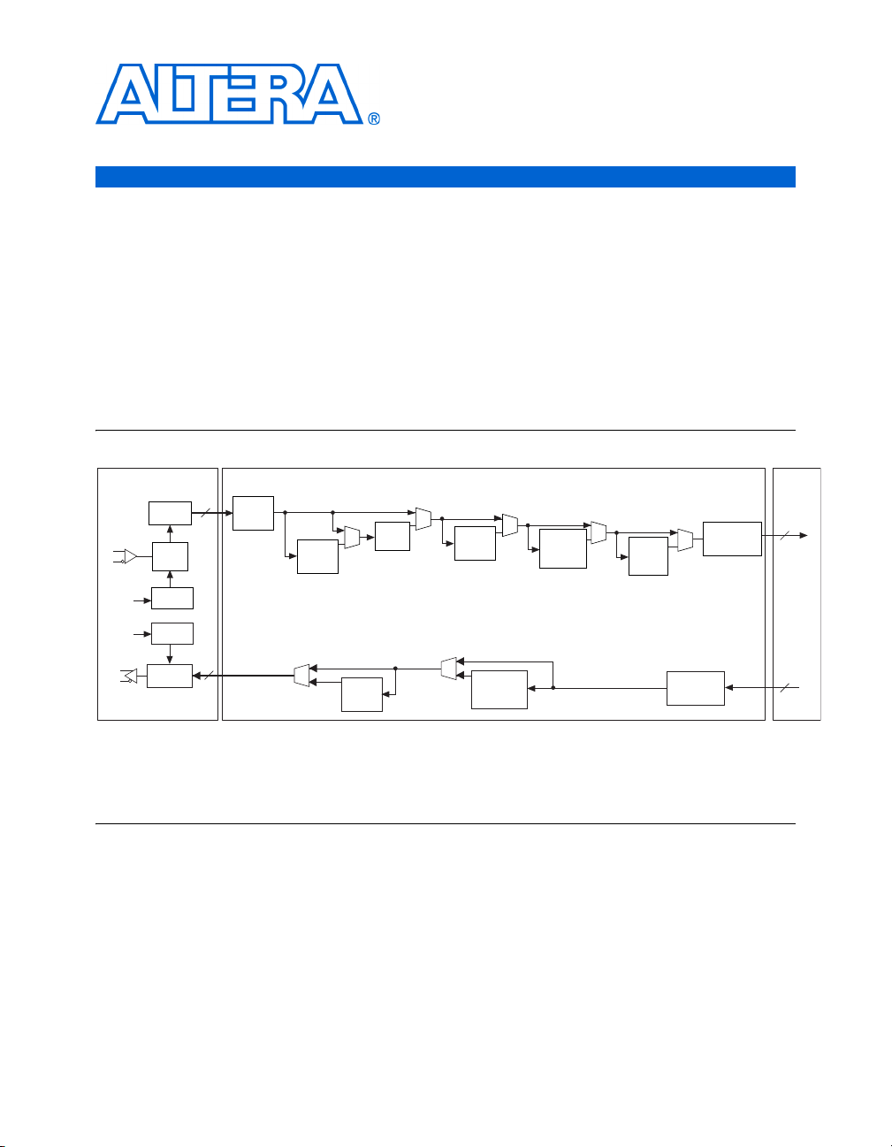
Figure 2–1 shows the function blocks that make up a transceiver channel
within the Stratix II GX device.
Figure 2–1. Stratix II GX Transceiver Block Diagram
Notes to Figure 2–1:
(1) n represents the number of bits in each word that need to be serialized by the transmitter portion of the PMA or have
been deserialized by the receiver portion of the PMA. n = 8, 10, 16, or 20.
(2) m represents the number of bits in the word that pass between the FPGA logic and the PCS portion of the transceiver.
m = 8, 10, 16, 20, 32, or 40.
Transceivers within each block are independent and have their own set of
dividers. Therefore, each transceiver can operate at different frequencies.
Altera Corporation 2–1
October 2007
Each block can select from two reference clocks to provide two clock
domains that each transceiver can select from.
Page 20
Transceivers
There are up to 20 transceiver channels available on a single Stratix II GX
device. Table 2–1 shows the number of transceiver channels and their
serial bandwidth for each Stratix II GX device.
Table 2–1. Stratix II GX Transceiver Channels
Device
EP2SGX30C 4 51 Gbps
EP2SGX60C 4 51 Gbps
EP2SGX30D 8 102 Gbps
EP2SGX60D 8 102 Gbps
EP2SGX60E 12 153 Gbps
EP2SGX90E 12 153 Gbps
EP2SGX90F 16 204 Gbps
EP2SGX130G 20 255 Gbps
Number of Transceiver
Channels
Serial Bandwidth
(Full Duplex)
Figure 2–2 shows the elements of the transceiver block, including the four
transceiver channels, supporting logic, and I/O buffers. Each transceiver
channel consists of a receiver and transmitter. The supporting logic
contains two transmitter PLLs to generate the high-speed clock(s) used by
the four transmitters within that block. Each of the four transmitter
channels has its own individual clock divider. The four receiver PLLs
within each transceiver block generate four recovered clocks. The
transceiver channels can be configured in one of the following functional
modes:
■ PCI Express (PIPE)
■ OIF CEI PHY Interface
■ SONET/SDH
■ Gigabit Ethernet (GIGE)
■ XAUI
■ Basic (600 Mbps to 3.125 Gbps single-width mode and 1 Gbps to
6.375 Gbps double-width mode)
■ SDI (HD, 3G)
■ CPRI (614 Mbps, 1228 Mbps, 2456 Mbps)
■ Serial RapidIO (1.25 Gbps, 2.5 Gbps, 3.125 Gbps)
2–2 Altera Corporation
Stratix II GX Device Handbook, Volume 1 October 2007
Page 21
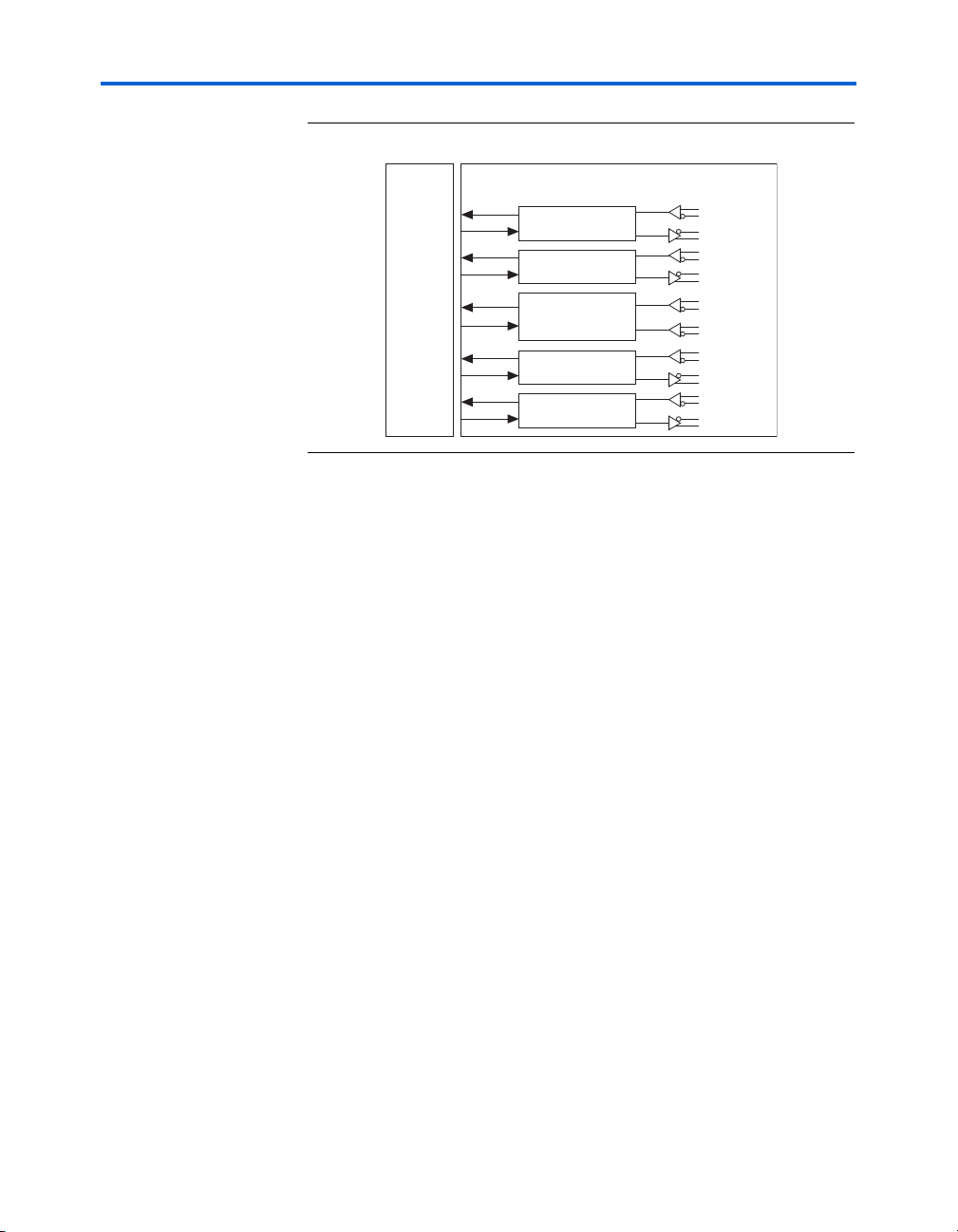
Stratix II GX Architecture
Channel 1
Channel 0
Channel 2
Supporting Blocks
(PLLs, State Machines,
Programming)
Channel 3
RX1
TX1
RX0
TX0
RX2
TX2
RX3
TX3
REFCLK_1
REFCLK_0
Transceiver BlockStratix II GX
Logic Array
Figure 2–2. Elements of the Transceiver Block
Each Stratix II GX transceiver channel consists of a transmitter and
receiver. The transceivers are grouped in four and share PLL resources.
Each transmitter has access to one of two PLLs. The transmitter contains
the following:
■ Transmitter phase compensation first-in first-out (FIFO) buffer
■ Byte serializer (optional)
■ 8B/10B encoder (optional)
■ Serializer (parallel-to-serial converter)
■ Transmitter differential output buffer
The receiver contains the following:
■ Receiver differential input buffer
■ Receiver lock detector and run length checker
■ Clock recovery unit (CRU)
■ Deserializer
■ Pattern detector
■ Word aligner
■ Lane deskew
■ Rate matcher (optional)
■ 8B/10B decoder (optional)
Altera Corporation 2–3
October 2007 Stratix II GX Device Handbook, Volume 1
■ Byte deserializer (optional)
■ Byte ordering
■ Receiver phase compensation FIFO buffer
Designers can preset Stratix II GX transceiver functions using the
®
Quartus
differential output voltage (V
Stratix II GX transceiver channel supports various loopback modes and is
II software. In addition, pre-emphasis, equalization, and
) are dynamically programmable. Each
OD
Page 22

Transceivers
capable of built-in self test (BIST) generation and verification. The
ALT2GXB megafunction in the Quartus II software provides a
step-by-step menu selection to configure the transceiver.
Figure 2–1 shows the block diagram for the Stratix II GX transceiver
channel. Stratix II GX transceivers provide PCS and PMA
implementations for all supported protocols. The PCS portion of the
transceiver consists of the word aligner, lane deskew FIFO buffer, rate
matcher FIFO buffer, 8B/10B encoder and decoder, byte serializer and
deserializer, byte ordering, and phase compensation FIFO buffers.
Each Stratix II GX transceiver channel is also capable of BIST generation
and verification in addition to various loopback modes. The PMA portion
of the transceiver consists of the serializer and deserializer, the CRU, and
the high-speed differential transceiver buffers that contain pre-emphasis,
programmable on-chip termination (OCT), programmable voltage
output differential (V
), and equalization.
OD
Transmitter Path
This section describes the data path through the Stratix II GX transmitter.
The Stratix II GX transmitter contains the following modules:
■ Transmitter PLLs
■ Access to one of two PLLs
■ Transmitter logic array interface
■ Transmitter phase compensation FIFO buffer
■ Byte serializer
■ 8B/10B encoder
■ Serializer (parallel-to-serial converter)
■ Transmitter differential output buffer
Transmitter PLLs
Each transceiver block has two transmitter PLLs which receive two
reference clocks to generate timing and the following clocks:
■ High-speed clock used by the serializer to transmit the high-speed
differential transmitter data
■ Low-speed clock to load the parallel transmitter data of the serializer
The serializer uses high-speed clocks to transmit data. The serializer is
also referred to as parallel in serial out (PISO). The high-speed clock is fed
to the local clock generation buffer. The local clock generation buffers
divide the high-speed clock on the transmitter to a desired frequency on
a per-channel basis. Figure 2–3 is a block diagram of the transmitter
clocks.
2–4 Altera Corporation
Stratix II GX Device Handbook, Volume 1 October 2007
Page 23
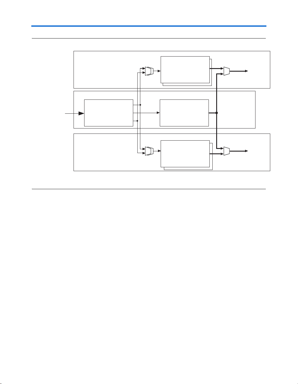
Figure 2–3. Clock Distribution for the Transmitters Note (1)
Transmitter PLL Block
Central Clock
Divider Block
TX Clock
Gen Block
TX Clock
Gen Block
Transmitter Channel [3..2]
Transmitter Channel [1..0]
Transmitter High-Speed &
Low-Speed Clocks
Transmitter High-Speed &
Low-Speed Clocks
Transmitter Local
Clock Divider Block
Transmitter Local
Clock Divider Block
Reference Clocks
(refclks,
Global Clock
(1)
,
Inter-Transceiver
Lines)
Central Block
Note to Figure 2–3:
(1) The global clock line must be driven by an input pin.
Stratix II GX Architecture
The transmitter PLLs in each transceiver block clock the PMA and PCS
circuitry in the transmit path. The Quartus II software automatically
powers down the transmitter PLLs that are not used in the design.
Figure 2–4 is a block diagram of the transmitter PLL.
The transmitter phase/frequency detector references the clock from one
of the following sources:
■ Reference clocks
■ Reference clock from the adjacent transceiver block
■ Inter-transceiver block clock lines
■ Global clock line driven by input pin
Two reference clocks, REFCLK0 and REFCLK1, are available per
transceiver block. The inter-transceiver block bus allows multiple
transceivers to use the same reference clocks. Each transceiver block has
Altera Corporation 2–5
October 2007 Stratix II GX Device Handbook, Volume 1
one outgoing reference clock which connects to one inter-transceiver
block line. The incoming reference clock can be selected from five
inter-transceiver block lines IQ[4..0] or from the global clock line that
is driven by an input pin.
Page 24
Transceivers
k
Figure 2–4. Transmitter PLL Block Note (1)
Transmitter PLL 0
÷
m
Inter-Transceiver Block
Routing (IQ[4:0])
Dedicated Local
REFCLK 0
Inter-Transceiver Block
Routing (IQ[4:0])
Dedicated Local
REFCLK 1
From PLD
÷
To Inter-Transceiver
Block Line
From PLD
÷
/22
2
INCLK
INCLK
PFD
PFD
Note to Figure 2–4:
(1) The global clock line must be driven by an input pin.
The transmitter PLLs support data rates up to 6.375 Gbps. The input clock
frequency is limited to 622.08 MHz. An optional pll_locked port is
available to indicate whether the transmitter PLL is locked to the
reference clock. Both transmitter PLLs have a programmable loop
bandwidth parameter that can be set to low, medium, or high. The loop
bandwidth parameter can be statically set in the Quartus II software.
up
CP+LF
dn
÷
m
up
CP+LF
dn
VCO
VCO
÷
L
Transmitter PLL 1
÷
L
High-Speed
Transmitter PLL0 Clock
High-Speed
Transmitter PLL Cloc
High-Speed
Transmitter PLL1 Clock
Table 2–2 lists the adjustable parameters in the transmitter PLL.
Table 2–2. Transmitter PLL Specifications
Parameter Specifications
Input reference frequency range 50 MHz to 622.08 MHz
Data rate support 600 Mbps to 6.375 Gbps
Multiplication factor (W) 1, 4, 5, 8, 10, 16, 20, 25
Bandwidth Low, medium, or high
2–6 Altera Corporation
Stratix II GX Device Handbook, Volume 1 October 2007
Page 25
Stratix II GX Architecture
Transmitter Phase Compensation FIFO Buffer
The transmitter phase compensation FIFO buffer resides in the
transceiver block at the PCS/FPGA boundary and cannot be bypassed.
This FIFO buffer compensates for phase differences between the
transmitter PLL clock and the clock from the PLD. After the transmitter
PLL has locked to the frequency and phase of the reference clock, the
transmitter FIFO buffer must be reset to initialize the read and write
pointers. After FIFO pointer initialization, the PLL must remain phase
locked to the reference clock.
Byte Serializer
The FPGA and transceiver block must maintain the same throughput. If
the FPGA interface cannot meet the timing margin to support the
throughput of the transceiver, the byte serializer is used on the
transmitter and the byte deserializer is used on the receiver.
The byte serializer takes words from the FPGA interface and converts
them into smaller words for use in the transceiver. The transmit data path
after the byte serializer is 8, 10, 16, or 20 bits. Refer to Table 2–3 for the
transmitter data with the byte serializer enabled. The byte serializer can
be bypassed when the data width is 8, 10, 16, or 20 bits at the FPGA
interface.
Table 2–3. Transmitter Data with the Byte Serializer Enabled
Input Data Width Output Data Width
16 bits 8 bits
20 bits 10 bits
32 bits 16 bits
40 bits 20 bits
If the byte serializer is disabled, the FPGA transmit data is passed without
data width conversion.
Altera Corporation 2–7
October 2007 Stratix II GX Device Handbook, Volume 1
Page 26
Transceivers
Table 2–4 shows the data path configurations for the Stratix II GX device
in single-width and double-width modes.
1 Refer to the section “8B/10B Encoder” on page 2–8 for a
description of the single- and double-width modes.
Table 2–4. Data Path Configurations Note (1)
Single-Width Mode Double-Width Mode
Parameter
Without Byte
Serialization/
Deserialization
Fabric to PCS data path width (bits) 8 or 10 16 or 20 16 or 20 32 or 40
Data rate range (Gbps) 0.6 to 2.5 0.6 to 3.125 1 to 5.0 1 to 6.375
PCS to PMA data path width (bits) 8 or 10 8 or 10 16 or 20 16 or 20
Byte ordering (1)
Data symbol A (MSB)
Data symbol B
Data symbol C
Data symbol D (LSB)
Note to Ta bl e 2 – 4 :
(1) Designs can use byte ordering when byte serialization and deserialization are used.
vvvv
With Byte
Serialization/
Deserialization
Without Byte
Serialization/
Deserialization
With Byte
Serialization/
Deserialization
vv
v
vv
vv
8B/10B Encoder
There are two different modes of operation for 8B/10B encoding.
Single-width (8-bit) mode supports natural data rates from 622 Mbps to
3.125 Gbps. Double-width (16-bit cascaded) mode supports data rates
above 3.125 Gbps. The encoded data has a maximum run length of five.
The 8B/10B encoder can be bypassed. Figure 2–5 diagrams the 10-bit
encoding process.
2–8 Altera Corporation
Stratix II GX Device Handbook, Volume 1 October 2007
Page 27
Figure 2–5. 8B/10B Encoding Process
t
Cascaded 8B/10B Conversion
G' F' E' D' C' B' A'H' G F E D C B AH
Parallel Data
CTRL[1..0] 15 14 13 12 11 10 9 8 7 6 5 4 3 2 1 0
LSB
MSB
g' f' i' e' d'
c'
b' a'
j'
h' g f iedc bajh
19 18 17 16 15 14 13 12 11 10 9 8 7 6 5 4 3 2 1 0
76543210
HGFED CB A
8B/10B Conversion
jhgfiedcba
9876543210
Stratix II GX Architecture
+
ctrl
MSB sent last
In single-width mode, the 8B/10B encoder generates a 10-bit code group
from the 8-bit data and 1-bit control identifier. In double-width mode,
there are two 8B/10B encoders that are cascaded together and generate a
20-bit (2 × 10-bit) code group from the 16-bit (2 × 8-bit) data + 2-bit
(2 × 1-bit) control identifier. Figure 2–6 shows the 20-bit encoding
process. The 8B/10B encoder conforms to the IEEE 802.3 1998 edition
standards.
Figure 2–6. 16-Bit to 20-Bit Encoding Process
LSB sent firs
Upon power on or reset, the 8B/10B encoder has a negative disparity
which chooses the 10-bit code from the RD-column. However, the
running disparity can be changed via the tx_forcedisp and
tx_dispval ports.
Altera Corporation 2–9
October 2007 Stratix II GX Device Handbook, Volume 1
Page 28
Transceivers
Transmit State Machine
The transmit state machine operates in either PCI Express mode, XAUI
mode, or GIGE mode, depending on the protocol used. The state machine
is not utilized for certain protocols, such as SONET.
GIGE Mode
In GIGE mode, the transmit state machine converts all idle ordered sets
(/K28.5/, /Dx.y/) to either /I1/ or /I2/ ordered sets. /I1/ consists of a
negative-ending disparity /K28.5/ (denoted by /K28.5/-) followed by a
neutral /D5.6/. /I2/ consists of a positive-ending disparity /K28.5/
(denoted by /K28.5/+) and a negative-ending disparity /D16.2/
(denoted by /D16.2/-). The transmit state machines do not convert any of
the ordered sets to match /C1/ or /C2/, which are the configuration
ordered sets. (/C1/ and /C2/ are defined by [/K28.5/, /D21.5/] and
[/K28.5/, /D2.2/], respectively). Both the /I1/ and /I2/ ordered sets
guarantee a negative-ending disparity after each ordered set.
XAUI Mode
The transmit state machine translates the XAUI XGMII code group to the
XAUI PCS code group. Table 2–5 shows the code conversion.
Table 2–5. Code Conversion
XGMII TXC XGMII TXD PCS Code-Group Description
0 00 through FF Dxx.y Normal data
1 07 K28.0 or K28.3 or
1 07 K28.5 Idle in ||T||
1 9C K28.4 Sequence
1 FB K27.7 Start
1 FD K29.7 Terminate
1 FE K30.7 Error
1 See IEEE 802.3
reserved code
groups
1 Other value K30.7 Invalid XGMII character
K28.5
See IEEE 802.3
reserved code groups
Idle in ||I||
Reserved code groups
The XAUI PCS idle code groups, /K28.0/ (/R/) and /K28.5/ (/K/), are
7
automatically randomized based on a PRBS7 pattern with an x
+ x6 + 1
polynomial. The /K28.3/ (/A/) code group is automatically generated
between 16 and 31 idle code groups. The idle randomization on the /A/,
/K/, and /R/ code groups is done automatically by the transmit state
machine.
2–10 Altera Corporation
Stratix II GX Device Handbook, Volume 1 October 2007
Page 29
Stratix II GX Architecture
D7
D6
D5
D4
D3
D2
D1
D0
D7
D6
D5
D4
D3
D2
D1
D0
Low-speed
parallel clock
High-speed
serial clock
Serial data
out (to output
buffer)
D8
D9
D8
D9
10
Serializer (Parallel-to-Serial Converter)
The serializer converts the parallel 8, 10, 16, or 20-bit data into a serial data
bit stream, transmitting the least significant bit (LSB) first. The serialized
data stream is then fed to the high-speed differential transmit buffer.
Figure 2–7 is a diagram of the serializer.
Figure 2–7. Serializer Note (1)
Note to Figure 2–7:
(1) This is a 10-bit serializer. The serializer can also convert 8, 16, and 20 bits of data.
Transmit Buffer
The Stratix II GX transceiver buffers support the 1.2- and 1.5-V PCML
I/O standard at rates up to 6.375 Gbps. The common mode voltage (V
of the output driver is programmable. The following V
available when the buffer is in 1.2- and 1.5-V PCML.
■ V
■ V
= 0.6 V
CM
= 0.7 V
CM
values are
CM
CM
Altera Corporation 2–11
October 2007 Stratix II GX Device Handbook, Volume 1
)
Page 30
Transceivers
Serializer
Programmable
Termination
Programmable
Pre-Emphasis
Output Buffer
Output
Pins
Programmable
Output
Driver
f Refer to the Stratix II GX Transceiver Architecture Overview chapter in
volume 2 of the Stratix II GX Handbook.
The output buffer, as shown in Figure 2–8, is directly driven by the
high-speed data serializer and consists of a programmable output driver,
a programmable pre-emphasis circuit, a programmable termination, and
a programmable V
Figure 2–8. Output Buffer
CM
.
Programmable Output Driver
The programmable output driver can be set to drive out differentially
200 to 1,400 mV. The differential output voltage (V
) can be changed
OD
dynamically, or statically set by using the ALT2GXB megafunction or
through I/O pins.
The output driver may be programmed with four different differential
termination values:
■ 100 Ω
2–12 Altera Corporation
Stratix II GX Device Handbook, Volume 1 October 2007
■ 120 Ω
■ 150 Ω
■ External termination
Page 31

Stratix II GX Architecture
V
MAX
V
MAX
V
MIN
V
MIN
Pre-Emphasis % = (
− 1) × 100
Differential signaling conventions are shown in Figure 2–9. The
differential amplitude represents the value of the voltage between the
true and complement signals. Peak-to-peak differential voltage is defined
as 2 × (V
HIGH
– V
mode voltage is the average of V
) = 2 × single-ended voltage swing. The common
LOW
high
and V
low
.
Figure 2–9. Differential Signaling
Single-Ended Waveform
True
Complement
V
high
+V
OD
-
V
low
V
= V
OD
high
(Differential)
−
V
low
Differential Waveform
+V
OD
2 * V
OD
+400
0-V Differential
-V
OD
−400
Programmable Pre-Emphasis
The programmable pre-emphasis module controls the output driver to
boost the high frequency components, and compensate for losses in the
transmission medium, as shown in Figure 2–10. The pre-emphasis is set
statically using the ALT2GXB megafunction or dynamically through the
dynamic reconfiguration controller.
Figure 2–10. Pre-Emphasis Signaling
Altera Corporation 2–13
October 2007 Stratix II GX Device Handbook, Volume 1
Page 32

Transceivers
Programmable
Output
Driver
50, 60, or 75
9
V
CM
Pre-emphasis percentage is defined as (V
is the differential emphasized voltage (peak-to-peak) and V
V
MAX
MAX/VMIN
– 1) × 100, where
MIN
is
the differential steady-state voltage (peak-to-peak).
Programmable Termination
The programmable termination can be statically set in the Quartus II
software. The values are 100 Ω, 120 Ω , 150 Ω , and external termination.
Figure 2–11 shows the setup for programmable termination.
Figure 2–11. Programmable Transmitter Terminations
PCI Express Receiver Detect
The Stratix II GX transmitter buffer has a built-in receiver detection circuit
for use in PIPE mode. This circuit provides the ability to detect if there is
a receiver downstream by sending out a pulse on the channel and
monitoring the reflection. This mode requires the transmitter buffer to be
tri-stated (in electrical idle mode).
PCI Express Electric Idles (or Individual Transmitter Tri-State)
The Stratix II GX transmitter buffer supports PCI Express electrical idles.
This feature is only active in PIPE mode. The tx_forceelecidle port
puts the transmitter buffer in electrical idle mode. This port is available in
all PCI Express power-down modes and has specific usage in each mode.
Receiver Path
This section describes the data path through the Stratix II GX receiver. The
Stratix II GX receiver consists of the following blocks:
■ Receiver differential input buffer
■ Receiver PLL lock detector, signal detector, and run length checker
■ Clock/data recovery (CRU) unit
■ Deserializer
■ Pattern detector
■ Word aligner
2–14 Altera Corporation
Stratix II GX Device Handbook, Volume 1 October 2007
Page 33

Stratix II GX Architecture
■ Lane deskew
■ Rate matcher
■ 8B/10B decoder
■ Byte deserializer
■ Byte ordering
■ Receiver phase compensation FIFO buffer
Receiver Input Buffer
The Stratix II GX receiver input buffer supports the 1.2-V and 1.5-V
PCML I/O standard at rates up to 6.375 Gbps. The common mode voltage
of the receiver input buffer is programmable between 0.85 V and 1.2 V.
You must select the 0.85 V common mode voltage for AC- and
DC-coupled PCML links and the 1.2 V common mode voltage for
DC-coupled LVDS links.
The receiver has programmable on-chip 100-, 120-, or 150-Ω differential
termination for different protocols, as shown in Figure 2–12. The
receiver’s internal termination can be disabled if external terminations
and biasing are provided. The receiver and transmitter differential
termination resistances can be set independently of each other.
Figure 2–12. Receiver Input Buffer
Programmable
Termination
Input
Pins
Programmable
Equalizer
Differential
Input
Buffer
Programmable Termination
The programmable termination can be statically set in the Quartus II
software. Figure 2–13 shows the setup for programmable receiver
termination. The termination can be disabled if external termination is
provided.
Altera Corporation 2–15
October 2007 Stratix II GX Device Handbook, Volume 1
Page 34

Transceivers
Transmission
Line
C1
R1/R2 = 1K
V
DD
× {R2/(R1 + R 2)} = 0.85/1.2 V
50/60/75-
Ω
Termination
Resistance
R1
R2
V
DD
Receiver External Termination
and Biasing
Stratix II GX Device
Receiver External Termination
and Biasing
RXIP
RXIN
Receiver
Figure 2–13. Programmable Receiver Termination
Differential
50, 60, or 75 Ω
50, 60, or 75 Ω
V
CM
Input
Buffer
If a design uses external termination, the receiver must be externally
terminated and biased to 0.85 V or 1.2 V. Figure 2–14 shows an example
of an external termination and biasing circuit.
Figure 2–14. External Termination and Biasing Circuit
2–16 Altera Corporation
Programmable Equalizer
The Stratix II GX receivers provide a programmable receive equalization
feature to compensate the effects of channel attenuation for high-speed
signaling. PCB traces carrying these high-speed signals have low-pass
filter characteristics. The impedance mismatch boundaries can also cause
signal degradation. The equalization in the receiver diminishes the lossy
attenuation effects of the PCB at high frequencies.
Stratix II GX Device Handbook, Volume 1 October 2007
Page 35

Stratix II GX Architecture
1 The Stratix II GX receivers also have adaptive equalization
capability that adjusts the equalization levels to compensate for
changing link characteristics. The adaptive equalization can be
powered down dynamically after it selects the appropriate
equalization levels.
The receiver equalization circuit is comprised of a programmable
amplifier. Each stage is a peaking equalizer with a different center
frequency and programmable gain. This allows varying amounts of gain
to be applied, depending on the overall frequency response of the channel
loss. Channel loss is defined as the summation of all losses through the
PCB traces, vias, connectors, and cables present in the physical link.
Figure 2–15 shows the frequency response for the 16 programmable
settings allowed by the Quartus II software for Stratix II GX devices.
Figure 2–15. Frequency Response
High
Medium
Low
Bypass EQ
Receiver PLL and CRU
Each transceiver block has four receiver PLLs, lock detectors, signal
detectors, run length checkers, and CRU units, each of which is dedicated
to a receive channel. If the receive channel associated with a particular
receiver PLL or CRU is not used, the receiver PLL and CRU are powered
down for the channel. Figure 2–16 shows the receiver PLL and CRU
circuits.
Altera Corporation 2–17
October 2007 Stratix II GX Device Handbook, Volume 1
Page 36

Transceivers
rx_cruclk
CP+LF
Up
Down
VCO
÷m
÷1, 4, 5, 8, 10, 16, 20, or 25
rx_datain
High Speed RCVD_CLK
Low Speed RCVD_CLK
Down
Up
rx_locktorefclk
rx_rlv[ ]
rx_locktodata
rx_freqlocked
Clock Recovery Unit (CRU)
PFD
÷L
÷2÷N
÷1, 2, 4
÷1, 2, 4
rx_pll_locked
Figure 2–16. Receiver PLL and CRU
The receiver PLLs and CRUs can support frequencies up to 6.375 Gbps.
The input clock frequency is limited to the full clock range of 50 to
622 MHz but only when using REFCLK0 or REFCLK1. An optional
RX_PLL_LOCKED port is available to indicate whether the PLL is locked
to the reference clock. The receiver PLL has a programmable loop
bandwidth which can be set to low, medium, or high. The Quartus II
software can statically set the loop bandwidth parameter.
All the parameters listed are programmable in the Quartus II software.
The receiver PLL has the following features:
■ Operates from 600 Mbps to 6.375 Gbps.
■ Uses a reference clock between 50 MHz and 622.08 MHz.
■ Programmable bandwidth settings: low, medium, and high.
■ Programmable rx_locktorefclk (forces the receiver PLL to lock
to the reference clock) and rx_locktodata (forces the receiver PLL
to lock to the data).
■ The voltage-controlled oscillator (VCO) operates at half rate and has
two modes. These modes are for low or high frequency operation
and provide optimized phase-noise performance.
■ Programmable frequency multiplication W of 1, 4, 5, 8, 10, 16, 20, and
25. Not all settings are supported for any particular frequency.
■ Two lock indication signals are provided. They are found in PFD
mode (lock-to-reference clock), and PD (lock-to-data).
2–18 Altera Corporation
Stratix II GX Device Handbook, Volume 1 October 2007
Page 37

Stratix II GX Architecture
The CRU has a built-in switchover circuit to select whether the PLL VCO
is aligned by the reference clock or the data. The optional port
rx_freqlocked monitors when the CRU is in locked-to-data mode.
In the automatic mode, the CRU PLL must be within the prescribed PPM
frequency threshold setting of the CRU reference clock for the CRU to
switch from locked-to-reference to locked-to-data mode.
The automatic switchover circuit can be overridden by using the optional
ports rx_locktorefclk and rx_locktodata. Table 2–6 shows the
possible combinations of these two signals.
Table 2–6. Receiver Lock Combinations
rx_locktodata rx_locktorefclk VCO (Lock to Mode)
00 Auto
0 1 Reference clock
1x Data
If the rx_locktorefclk and rx_locktodata ports are not used, the
default is auto mode.
Deserializer (Serial-to-Parallel Converter)
The deserializer converts a serial bitstream into 8, 10, 16, or 20 bits of
parallel data. The deserializer receives the LSB first. Figure 2–17 shows
the deserializer.
Altera Corporation 2–19
October 2007 Stratix II GX Device Handbook, Volume 1
Page 38

Transceivers
High-speed
serial clock
D7
D6
D5
D4
D3
D2
D1
D0
D8
D9
Low-speed
parallel clock
D7
D6
D5
D4
D3
D2
D1
D0
D8
D9
10
Figure 2–17. Deserializer Note (1)
Note to Figure 2–17:
(1) This is a 10-bit deserializer. The deserializer can also convert 8, 16, or 20 bits of data.
Word Aligner
The deserializer block creates 8-, 10-, 16-, or 20-bit parallel data. The
deserializer ignores protocol symbol boundaries when converting this
data. Therefore, the boundaries of the transferred words are arbitrary. The
word aligner aligns the incoming data based on specific byte or word
boundaries. The word alignment module is clocked by the local receiver
2–20 Altera Corporation
Stratix II GX Device Handbook, Volume 1 October 2007
recovered clock during normal operation. All the data and programmed
patterns are defined as big-endian (most significant word followed by
least significant word). Most-significant-bit-first protocols such as
SONET/SDH should reverse the bit order of word align patterns
programmed.
Page 39

Stratix II GX Architecture
Word
Aligner
datain dataout
bitslip
enapatternalign
syncstatus
patterndetect
clock
This module detects word boundaries for the 8B/10B-based protocols,
SONET, 16-bit, and 20-bit proprietary protocols. This module is also used
to align to specific programmable patterns in PRBS7/23 test mode.
Pattern Detection
The programmable pattern detection logic can be programmed to align
word boundaries using a single 7-, 8-, 10-, 16-, 20, or 32-bit pattern. The
pattern detector can either do an exact match, or match the exact pattern
and the complement of a given pattern. Once the programmed pattern is
found, the data stream is aligned to have the pattern on the LSB portion
of the data output bus.
XAUI, GIGE, PCI Express, and Serial RapidIO standards have embedded
state machines for symbol boundary synchronization. These standards
use K28.5 as their 10-bit programmed comma pattern. Each of these
standards uses different algorithms before signaling symbol boundary
acquisition to the FPGA.
The pattern detection logic searches from the LSB to the most significant
bit (MSB). If multiple patterns are found within the search window, the
pattern in the lower portion of the data stream (corresponding to the
pattern received earlier) is aligned and the rest of the matching patterns
are ignored.
Once a pattern is detected and the data bus is aligned, the word boundary
is locked. The two detection status signals (rx_syncstatus and
rx_patterndetect) indicate that an alignment is complete.
Figure 2–18 is a block diagram of the word aligner.
Figure 2–18. Word Aligner
Altera Corporation 2–21
October 2007 Stratix II GX Device Handbook, Volume 1
Page 40

Transceivers
Control and Status Signals
The rx_enapatternalign signal is the FPGA control signal that
enables word alignment in non-automatic modes. The
rx_enapatternalign signal is not used in automatic modes (PCI
Express, XAUI, GIGE, CPRI, and Serial RapidIO).
In manual alignment mode, after the rx_enapatternalign signal is
activated, the rx_syncstatus signal goes high for one parallel clock
cycle to indicate that the alignment pattern has been detected and the
word boundary has been locked. If the rx_enapatternalign is
deactivated, the rx_syncstatus signal acts as a re-synchronization
signal to signify that the alignment pattern has been detected but not
locked on a different word boundary.
When using the synchronization state machine, the rx_syncstatus
signal indicates the link status. If the rx_syncstatus signal is high, link
synchronization is achieved. If the rx_syncstatus signal is low,
synchronization has not yet been achieved, or there were enough code
group errors to lose synchronization.
In some modes, the rx_enapatternalign signal can be configured to
operate as a rising edge signal.
f For more information on manual alignment modes, refer to the
Stratix II GX Device Handbook, volume 2.
When the rx_enapatternalign signal is sensitive to the rising edge,
each rising edge triggers a new boundary alignment search, clearing the
rx_syncstatus signal.
The rx_patterndetect signal pulses high during a new alignment,
and also whenever the alignment pattern occurs on the current word
boundary.
SONET/SDH
In all the SONET/SDH modes, you can configure the word aligner to
either align to A1A2 or A1A1A2A2 patterns. Once the pattern is found,
the word boundary is aligned and the word aligner asserts the
rx_patterndetect signal for one clock cycle.
2–22 Altera Corporation
Stratix II GX Device Handbook, Volume 1 October 2007
Page 41

Stratix II GX Architecture
Programmable Run Length Violation
The word aligner supports a programmable run length violation counter.
Whenever the number of the continuous ‘0’ (or ‘1’) exceeds a user
programmable value, the rx_rlv signal goes high for a minimum pulse
width of two recovered clock cycles. The maximum run values supported
are shown in Table 2–7.
Table 2–7. Maximum Run Length (UI)
Mode
PMA Serialization
8 Bit 10 Bit 16 Bit 20 Bit
Single-Width 128 160 — —
Double-Width — — 512 640
Running Disparity Check
The running disparity error rx_disperr and running disparity value
rx_runningdisp are sent along with aligned data from the 8B/10B
decoder to the FPGA. You can ignore or act on the reported running
disparity value and running disparity error signals.
Bit-Slip Mode
The word aligner can operate in either pattern detection mode or in
bit-slip mode.
The bit-slip mode provides the option to manually shift the word
boundary through the FPGA. This feature is useful for:
■ Longer synchronization patterns than the pattern detector can
accommodate
■ Scrambled data stream
■ Input stream consisting of over-sampled data
This feature can be applied at 10-bit and 16-bit data widths.
The word aligner outputs a word boundary as it is received from the
analog receiver after reset. You can examine the word and search its
boundary in the FPGA. To do so, assert the rx_bitslip signal. The
rx_bitslip signal should be toggled and held constant for at least two
FPGA clock cycles.
For every rising edge of the rx_bitslip signal, the current word
boundary is slipped by one bit. Every time a bit is slipped, the bit received
earliest is lost. If bit slipping shifts a complete round of bus width, the
word boundary is back to the original boundary.
Altera Corporation 2–23
October 2007 Stratix II GX Device Handbook, Volume 1
Page 42

Transceivers
KRKKKRRRKKRA
Lane 3
KRKKKRRRKKRA
Lane 2
KRKKKRRRKKRA
Lane 1
KRKKKRRRKKRA
Lane 0
KRKKKRRRKKRA
Lane 3
KRKKKRRRKKRA
Lane 2
KRKKKRRRKKRA
Lane 1
KRKKKRRRKKRA
Lane 0
Before
After
The rx_syncstatus signal is not available in bit-slipping mode.
Channel Aligner
The channel aligner is available only in XAUI mode and aligns the signals
of all four channels within a transceiver. The channel aligner follows the
IEEE 802.3ae, clause 48 specification for channel bonding.
The channel aligner is a 16-word FIFO buffer with a state machine
controlling the channel bonding process. The state machine looks for an
/A/ (/K28.3/) in each channel, and aligns all the /A/ code groups in the
transceiver. When four columns of /A/ (denoted by //A//) are
detected, the rx_channelaligned signal goes high, signifying that all
the channels in the transceiver have been aligned. The reception of four
consecutive misaligned /A/ code groups restarts the channel alignment
sequence and sends the rx_channelaligned signal low.
Figure 2–19 shows misaligned channels before the channel aligner and
the aligned channels after the channel aligner.
Figure 2–19. Before and After the Channel Aligner
2–24 Altera Corporation
Stratix II GX Device Handbook, Volume 1 October 2007
Page 43

Stratix II GX Architecture
Rate Matcher
Rate matcher is available in Basic, PCI Express, XAUI, and GIGE modes
and consists of a 20-word deep FIFO buffer and a FIFO controller.
Figure 2–20 shows the implementation of the rate matcher in the
Stratix II GX device.
Figure 2–20. Rate Matcher
dataoutdatain
Rate
Matcher
wrclock
rdclock
In a multi-crystal environment, the rate matcher compensates for up to a
± 300-PPM difference between the source and receiver clocks. Table 2–8
shows the standards supported and the PPM for the rate matcher
tolerance.
Table 2–8. Rate Matcher PPM Support Note (1)
Standard PPM
XAUI ± 100
PCI Express (PIPE) ± 300
GIGE ± 100
Basic Double-Width ± 300
Note to Table 2–8:
(1) Refer to the Stratix II GX Transceiver User Guide for the Altera®-defined scheme.
Basic Mode
In Basic mode, you can program the skip and control pattern for rate
matching. In single-width Basic mode, there is no restriction on the
deletion of a skip character in a cluster. The rate matcher deletes the skip
characters as long as they are available. For insertion, the rate matcher
inserts skip characters such that the number of skip characters at the
output of rate matcher does not exceed five. In double-width mode, the
rate matcher deletes skip character when they appear as pairs in the
upper and lower bytes. There are no restrictions on the number of skip
characters that are deleted. The rate matcher inserts skip characters as
pairs.
Altera Corporation 2–25
October 2007 Stratix II GX Device Handbook, Volume 1
Page 44

Transceivers
GIGE Mode
In GIGE mode, the rate matcher adheres to the specifications in clause 36
of the IEEE 802.3 documentation for idle additions or removals. The rate
matcher performs clock compensation only on /I2/ ordered sets,
composed of a /K28.5/+ followed by a /D16.2/-. The rate matcher does
not perform clock compensation on any other ordered set combinations.
An /I2/ is added or deleted automatically based on the number of words
in the FIFO buffer. A K28.4 is given at the control and data ports when the
FIFO buffer is in an overflow or underflow condition.
XAUI Mode
In XAUI mode, the rate matcher adheres to clause 48 of the IEEE 802.3ae
specification for clock rate compensation. The rate matcher performs
clock compensation on columns of /R/ (/K28.0/), denoted by //R//.
An //R// is added or deleted automatically based on the number of
words in the FIFO buffer.
PCI Express Mode
PCI Express mode operates at a data rate of 2.5 Gbps, and supports lane
widths of ×1, ×2, ×4, and ×8. The rate matcher can support up to
± 300-PPM differences between the upstream transmitter and the
receiver. The rate matcher looks for the skip ordered sets (SOS), which
usually consist of a /K28.5/ comma followed by three /K28.0/ skip
characters. The rate matcher deletes or inserts skip characters when
necessary to prevent the rate matching FIFO buffer from overflowing or
underflowing.
The Stratix II GX rate matcher in PCI Express mode has FIFO overflow
and underflow protection. In the event of a FIFO overflow, the rate
matcher deletes any data after the overflow condition to prevent FIFO
pointer corruption until the rate matcher is not full. In an underflow
condition, the rate matcher inserts 9'h1FE (/K30.7/) until the FIFO is not
empty. These measures ensure that the FIFO can gracefully exit the
overflow and underflow condition without requiring a FIFO reset.
8B/10B Decoder
The 8B/10B decoder (Figure 2–21) is part of the Stratix II GX transceiver
digital blocks (PCS) and lies in the receiver path between the rate matcher
and the byte deserializer blocks. The 8B/10B decoder operates in
single-width and double-width modes, and can be bypassed if the
8B/10B decoding is not necessary. In single-width mode, the 8B/10B
decoder restores the 8-bit data + 1-bit control identifier from the 10-bit
code. In double-width mode, there are two 8B/10B decoders in parallel,
which restores the 16-bit (2 × 8-bit) data + 2-bit (2 × 1-bit) control identifier
from the 20-bit (2 × 10-bit) code. This 8B/10B decoder conforms to the
IEEE 802.3 1998 edition standards.
2–26 Altera Corporation
Stratix II GX Device Handbook, Volume 1 October 2007
Page 45

Stratix II GX Architecture
8B/10B
Decoder
MSByte
datain[19..10]
To Byte
Deserializer
dataout[15..8]
Status Signals[1] (1)
8B/10B
Decoder
LSByte
datain[9..0]
dataout[7..0]
Status Signals[0]
From Rate
Matcher
(1)
Figure 2–21. 8B/10B Decoder
The 8B/10B decoder in single-width mode translates the 10-bit encoded
data into the 8-bit equivalent data or control code. The 10-bit code
received must be from the supported Dx.y or Kx.y list with the proper
disparity or error flags asserted. All 8B/10B control signals, such as
disparity error or control detect, are pipelined with the data and
edge-aligned with the data. Figure 2–22 shows how the 10-bit symbol is
decoded in the 8-bit data + 1-bit control indicator.
Figure 2–22. 8B/10B Decoder Conversion
jhgfiedcba
9876543210
MSB received last
8B/10B conversion
Parallel data
The 8B/10B decoder in double-width mode translates the 20-bit
(2 × 10-bits) encoded code into the 16-bit (2 × 8-bits) equivalent data or
control code. The 20-bit upper and lower symbols received must be from
the supported Dx.y or Kx.y list with the proper disparity or error flags
Altera Corporation 2–27
October 2007 Stratix II GX Device Handbook, Volume 1
76543210
HGFED CB A
LSB received first
+
ctrl
Page 46

Transceivers
19 18 17 16 15 14 13 12 11 10
Cascaded 8B/10B Conversion
j1h
1g1f1i1e1d1c1b1a1
MSB
LSB
15 14 13 13 11 10 9 8
H
1G1F1E1D1C1B1A1
CTRL[1..0]
9876543210
jhg fiedcba
7654321 0
HGFEDCB A
Parallel Data
asserted. All 8B/10B control signals, such as disparity error or control
detect, are pipelined with the data in the Stratix II GX receiver block and
are edge aligned with the data.
Figure 2–23 shows how the 20-bit code is decoded to the 16-bit data +
2-bit control indicator.
Figure 2–23. 20-Bit to 16-Bit Decoding Process
2–28 Altera Corporation
Stratix II GX Device Handbook, Volume 1 October 2007
There are two optional error status ports available in the 8B/10B decoder,
rx_errdetect and rx_disperr. These status signals are aligned with
the code group in which the error occurred.
Receiver State Machine
The receiver state machine operates in Basic, GIGE, PCI Express, and
XAUI modes. In GIGE mode, the receiver state machine replaces invalid
code groups with K30.7. In XAUI mode, the receiver state machine
translates the XAUI PCS code group to the XAUI XGMII code group.
Byte Deserializer
The byte deserializer widens the transceiver data path before the FPGA
interface. This reduces the rate at which the received data needs to be
clocked at in the FPGA logic. The byte deserializer block is available in
both single- and double-width modes.
The byte deserializer converts the one- or two-byte interface into a
two- or four-byte-wide data path from the transceiver to the FPGA logic
(see Table 2–9). The FPGA interface has a limit of 250 MHz, so the byte
deserializer is needed to widen the bus width at the FPGA interface and
Page 47

Stratix II GX Architecture
reduce the interface speed. For example, at 6.375 Gbps, the transceiver
logic has a double-byte-wide data path that runs at 318.75 MHz in a ×20
deserializer factor, which is above the maximum FPGA interface speed.
When using the byte deserializer, the FPGA interface width doubles to
40-bits (36-bits when using the 8B/10B encoder) and the interface speed
reduces to 159.375 MHz.
Table 2–9. Byte Deserializer Input and Output Widths
Input Data Width (Bits)
20 40
16 32
10 20
816
Deserialized Output Data Width to the
FPGA (Bits)
Byte Ordering Block
The byte ordering block shifts the byte order. A pre-programmed byte in
the input data stream is detected and placed in the least significant byte
of the output stream. Subsequent bytes start appearing in the byte
positions following the LSB. The byte ordering block inserts the
programmed PAD characters to shift the byte order pattern to the LSB.
®
Based on the setting in the MegaWizard
ordering block can be enabled either by the rx_syncstatus signal or by
the rx_enabyteord signal from the PLD. When the rx_syncstatus
signal is used as enable, the byte ordering block reorders the data only for
the first occurrence of the byte order pattern that is received after word
alignment is completed. You must assert rx_digitalreset to perform
byte ordering again. However, when the byte ordering block is controlled
by rx_enabyteord, the byte ordering block can be controlled by the
PLD logic dynamically. When you create your functional mode in the
MegaWizard, you can select byte ordering block only if rate matcher is
not selected.
Plug-In Manager, the byte
Receiver Phase Compensation FIFO Buffer
The receiver phase compensation FIFO buffer resides in the transceiver
block at the FPGA boundary and cannot be bypassed. This FIFO buffer
compensates for phase differences and clock tree timing skew between
the receiver clock domain within the transceiver and the receiver FPGA
clock after it has transferred to the FPGA.
Altera Corporation 2–29
October 2007 Stratix II GX Device Handbook, Volume 1
Page 48

Transceivers
When the FIFO pointers initialize, the receiver domain clock must remain
phase locked to receiver FPGA clock.
After resetting the receiver FIFO buffer, writing to the receiver FIFO
buffer begins and continues on each parallel clock. The phase
compensation FIFO buffer is eight words deep for PIPE mode and four
words deep for all other modes.
Loopback Modes
The Stratix II GX transceiver has built-in loopback modes for debugging
and testing. The loopback modes are configured in the Stratix II GX
ALT2GXB megafunction in the Quartus II software. The available
loopback modes are:
■ Serial loopback
■ Parallel loopback
■ Reverse serial loopback
■ Reverse serial loopback (pre-CDR)
■ PCI Express PIPE reverse parallel loopback (available only in PIPE
mode)
Serial Loopback
The serial loopback mode exercises all the transceiver logic, except for the
input buffer. Serial loopback is available for all non-PIPE modes. The
loopback function is dynamically enabled through the
rx_seriallpbken port on a channel-by-channel basis.
In serial loopback mode, the data on the transmit side is sent by the PLD.
A separate mode is available in the ALT2GXB megafunction under Basic
protocol mode, in which PRBS data is generated and verified internally in
the transceiver. The PRBS patterns available in this mode are shown in
Table 2–10.
Table 2–10 shows the BIST data output and verifier alignment pattern.
Table 2–10. BIST Data Output and Verifier Alignment Pattern
Parallel Data Width
Pattern Polynomial
8-Bit 10-Bit 16-Bit 20-Bit
PRBS-7 ×7 + ×6 + 1
PRBS-10 ×10 + ×7 + 1
2–30 Altera Corporation
Stratix II GX Device Handbook, Volume 1 October 2007
v
v
Page 49

Figure 2–24 shows the data path in serial loopback mode.
Transmitter Digital Logic
Receiver Digital Logic
Analog Receiver and
Transmitter Logic
FPGA
Logic
Array
BIST
Incremental
Generator
TX Phase
Compensation
FIFO
RX Phase
Compen-
sation
FIFO
Byte
Serializer
8B/10B
Encoder
Serializer
Serial
Loopback
BIST
PRBS
Verify
Clock
Recovery
Unit
Word
Aligner
Deskew
FIFO
8B/10B
Decoder
Byte
De-
serializer
Byte
Ordering
BIST
Incremental
Verify
Rate
Match
FIFO
De-
serializer
BIST
PRBS
Generator
20
Figure 2–24. Stratix II GX Block in Serial Loopback Mode with BIST and PRBS
Parallel Loopback
Stratix II GX Architecture
The parallel loopback mode exercises the digital logic portion of the
transceiver data path. The analog portions are not used in this loopback
path, and the received high-speed serial data is not retimed. This protocol
is available as one of the sub-protocols under Basic mode and can be used
only for Basic double-width mode.
In this loopback mode, the data from the internally available BIST
generator is transmitted. The data is looped back after the end of PCS and
before the PMA. On the receive side, an internal BIST verifier checks for
errors. This loopback enables you to verify the PCS block.
Altera Corporation 2–31
October 2007 Stratix II GX Device Handbook, Volume 1
Page 50

Transceivers
Figure 2–25 shows the data path in parallel loopback mode.
Figure 2–25. Stratix II GX Block in Parallel Loopback Mode
Transmitter Digital Logic
Incremental
Generator
FPGA
Logic
Array
Incremental
RX Phase
Compen-
Receiver Digital Logic
BIST
TX Phase
Compensation
FIFO
BIST
Verify
sation
FIFO
Analog Receiver and
Parallel
Loopback
Word
Aligner
Transmitter Logic
Serializer
De-
serializer
Byte
Serializer
Byte
Ordering
20
serializer
8B/10B
Encoder
Byte
De-
BIST PRBS
Generator
8B/10B
Decoder
Rate
Match
FIFO
Deskew
FIFO
BIST
PRBS
Verify
Reverse Serial Loopback
The reverse serial loopback mode uses the analog portion of the
transceiver. An external source (pattern generator or transceiver)
generates the source data. The high-speed serial source data arrives at the
high-speed differential receiver input buffer, passes through the CRU
unit, and the retimed serial data is looped back and transmitted though
the high-speed differential transmitter output buffer.
Clock
Recovery
Unit
2–32 Altera Corporation
Stratix II GX Device Handbook, Volume 1 October 2007
Page 51

Figure 2–26 shows the data path in reverse serial loopback mode.
Figure 2–26. Stratix II GX Block in Reverse Serial Loopback Mode
Stratix II GX Architecture
Transmitter Digital Logic
Incremental
Generator
FPGA
Logic
Array
Incremental
RX Phase
Compen-
Receiver Digital Logic
BIST
TX Phase
Compensation
FIFO
BIST
Verify
sation
FIFO
Analog Receiver and
Word
Aligner
Transmitter Logic
Serializer
De-
serializer
Byte
Serializer
Byte
Ordering
20
Byte
De-
serializer
8B/10B
Encoder
8B/10B
Decoder
BIST
PRBS
Generator
Rate
Match
FIFO
Deskew
FIFO
BIST
PRBS
Verify
Reverse Serial Pre-CDR Loopback
The reverse serial pre-CDR loopback mode uses the analog portion of the
transceiver. An external source (pattern generator or transceiver)
generates the source data. The high-speed serial source data arrives at the
high-speed differential receiver input buffer, loops back before the CRU
unit, and is transmitted though the high-speed differential transmitter
output buffer. It is for test or verification use only to verify the signal
being received after the gain and equalization improvements of the input
buffer. The signal at the output is not exactly what is received since the
signal goes through the output buffer and the VOD is changed to the
VOD setting level. The pre-emphasis settings have no effect.
Reverse
Serial
Loopback
Clock
Recovery
Unit
Altera Corporation 2–33
October 2007 Stratix II GX Device Handbook, Volume 1
Page 52

Transceivers
Figure 2–27 show the Stratix II GX block in reverse serial pre-CDR
loopback mode.
Figure 2–27. Stratix II GX Block in Reverse Serial Pre-CDR Loopback Mode
Transmitter Digital Logic
8B/10B
Decoder
BIST
PRBS
Generator
Rate
Match
FIFO
Deskew
FIFO
BIST
PRBS
Verify
Word
Aligner
FPGA
Logic
Array
BIST
Incremental
Generator
TX Phase
Compensation
BIST
Incremental
Verify
RX Phase
Compen-
sation
FIFO
FIFO
Byte
Serializer
Byte
Ordering
20
Byte
serializer
8B/10B
Encoder
De-
Receiver Digital Logic
PCI Express PIPE Reverse Parallel Loopback
This loopback mode, available only in PIPE mode, can be dynamically
enabled by the tx_detectrxloopback port of the PIPE interface.
Figure 2–28 shows the datapath for this mode.
Figure 2–28. Stratix II GX Block in PCI Express PIPE Reverse Parallel Loopback Mode
Transmitter Digital Logic
BIST
Incremental
Generator
BIST
PRBS
Generator
Analog Receiver and
Transmitter Logic
Serializer
Reverse
Serial
Pre-CDR
Loopback
Clock
De-
Recovery
serializer
Analog Receiver and
Transmitter Logic
Unit
FPGA
Logic
Array
TX Phase
Compensation
BIST
Incremental
Verify
RX Phase
Compen-
sation
FIFO
FIFO
Byte
Serializer
Byte
Ordering
20
serializer
8B/10B
Encoder
Byte
De-
PCI Express PIPE
Reverse Parallel
Loopback
8B/10B
Decoder
Rate
Match
FIFO
Deskew
FIFO
BIST
PRBS
Verify
Word
Aligner
Serializer
De-
serializer
Clock
Recovery
Unit
Receiver Digital Logic
2–34 Altera Corporation
Stratix II GX Device Handbook, Volume 1 October 2007
Page 53

Stratix II GX Architecture
Transceiver Clocking
Each Stratix II GX device transceiver block contains two transmitter PLLs
and four receiver PLLs. These PLLs can be driven by either of the two
reference clocks per transceiver block. These REFCLK signals can drive all
global clocks, transmitter PLL inputs, and all receiver PLL inputs.
Subsequently, the transmitter PLL output can only drive global clock
lines and the receiver PLL reference clock port. Only one of the two
reference clocks in a quad can drive the Inter Quad (I/Q) lines to clock the
PLLs in the other quads.
Figure 2–29 shows the inter-transceiver line connections as well as the
global clock connections for the EP2SGX130 device.
Altera Corporation 2–35
October 2007 Stratix II GX Device Handbook, Volume 1
Page 54

Transceivers
Transmitter
PLL 0
Transceiver Block 0
REFCLK0
4
Receiver
PLLs
Transmitter
PLL 1
REFCLK1
IQ[4..0]
IQ[4..0]
IQ[4..0]
Global clk line
To IQ0
Transmitter
PLL 0
Transceiver Block 1
4
Receiver
PLLs
Transmitter
PLL 1
IQ[4..0]
IQ[4..0]
IQ[4..0]
To IQ1
Transmitter
PLL 0
Transceiver Block 2
4
Receiver
PLLs
Transmitter
PLL 1
IQ[4..0]
IQ[4..0]
IQ[4..0]
To IQ4
Transmitter
PLL 0
Transceiver Block 3
4
Receiver
PLLs
Transmitter
PLL 1
IQ[4..0]
IQ[4..0]
IQ[4..0]
To IQ2
Transmitter
PLL 0
Transceiver Block 4
4
Receiver
PLLs
Transmitter
PLL 1
From Global Clock Line (3)
IQ[4..0]
IQ[4..0]
IQ[4..0]
To IQ3
IQ[4..0]
To PLD
Global Clocks
16 Interface Clocks
From Global
Clock Line (3)
÷2
REFCLK0
÷2
REFCLK0
÷2
REFCLK0
÷2
REFCLK0
÷2
÷2
REFCLK1
÷2
REFCLK1
÷2
REFCLK1
÷2
REFCLK1
÷2
Global clk line
Global clk line
Global clk line
Global clk line
Global clk line
Global clk line
Global clk line
Global clk line
Global clk line
From Global Clock Line (3)
From Global Clock Line (3)
From Global Clock Line (3)
From Global Clock Line (3)
Transceiver Clock Generator Block
Transceiver Clock Generator Block
Transceiver Clock Generator Block
Transceiver Clock Generator Block
Transceiver Clock Generator Block
Figure 2–29. EP2SGX130 Device Inter-Transceiver and Global Clock Connections
Notes to Figure 2–29:
(1) There are two transmitter PLLs in each transceiver block.
(2) There are four receiver PLLs in each transceiver block.
(3) The Global Clock line must be driven by an input pin.
2–36 Altera Corporation
Stratix II GX Device Handbook, Volume 1 October 2007
Page 55

Stratix II GX Architecture
GCLK[15..12]
GCLK[4..7]
GCLK[11..8]
GCLK[3..0]
Stratix II GX
Transceiver
Block
Stratix II GX
Transceiver
Block
12 6
11 5
CLK[7..4]
CLK[15..12]
CLK[3..0]
1
7
2
8
The receiver PLL can also drive the regional clocks and regional routing
adjacent to the associated transceiver block. Figure 2–30 shows which
global clock resource can be used by the recovered clock. Figure 2–31
shows which regional clock resource can be used by the recovered clock.
Figure 2–30. Stratix II GX Receiver PLL Recovered Clock to Global Clock
Connection Notes (1), (2)
Notes to Figure 2–30:
(1) CLK# pins are clock pins and their associated number. These are pins for global
and regional clocks.
(2) GCLK# pins are global clock pins.
Altera Corporation 2–37
October 2007 Stratix II GX Device Handbook, Volume 1
Page 56

Transceivers
Figure 2–31. Stratix II GX Receiver PLL Recovered Clock to Regional Clock
Connection Notes (1), (2)
CLK[15..12]
11 5
7
RCLK
[3..0]
RCLK
[31..28]
RCLK
[27..24]
RCLK
[23..20]
Stratix II GX
Transceiver
Block
CLK[3..0]
1
2
RCLK
[7..4]
RCLK
8
[11..8]
CLK[7..4]
RCLK
[15..12]
12 6
RCLK
[19..16]
Stratix II GX
Transceiver
Block
Notes to Figure 2–31:
(1) CLK# pins are clock pins and their associated number. These are pins for global
and local clocks.
(2) RCLK# pins are regional clock pins.
2–38 Altera Corporation
Stratix II GX Device Handbook, Volume 1 October 2007
Page 57

Table 2–11 summarizes the possible clocking connections for the
transceivers.
Table 2–11. Available Clocking Connections for Transceivers
Source
REFCLK[1..0]
Transmitter PLL
Receiver PLL
Global clock
(driven from an
input pin)
Inter-transceiver
lines
Transmitter
PLL
Receiver PLL Global Clock
vvvv v
vv
vv
Clock Resource for PLD-Transceiver Interface
For the regional or global clock network to route into the transceiver, a
local route input output (LRIO) channel is required. Each LRIO clock
region has up to eight clock paths and each transceiver block has a
maximum of eight clock paths for connecting with LRIO clocks. These
resources are limited and determine the number of clocks that can be used
between the PLD and transceiver blocks. Table 2–12 shows the number of
LRIO resources available for Stratix II GX devices with different numbers
of transceiver blocks.
Stratix II GX Architecture
Destination
Regional
Clock
vv
vv
Inter-Transceiver
Lines
Tables 2–12 through 2–15 show the connection of the LRIO clock resource
to the transceiver block.
Table 2–12. Available Clocking Connections for Transceivers in 2SGX30D
Clock Resource Transceiver
Region
Region0
8 LRIO clock
Region1
8 LRIO clock
Altera Corporation 2–39
October 2007 Stratix II GX Device Handbook, Volume 1
Global
Clock
v
v
Regional
Clock
RCLK 20-27
RCLK 12-19
Bank 13
8 Clock I/O
v
Bank 14
8 Clock I/O
v
Page 58

Transceivers
.
Table 2–13. Available Clocking Connections for Transceivers in 2SGX60E
Clock Resource Transceiver
Region
Region0
8 LRIO clock
Region1
8 LRIO clock
Region2
8 LRIO clock
Region3
8 LRIO clock
Global Clock
v
v
v
v
Regional
Clock
RCLK 20-27
RCLK 20-27
RCLK 12-19
RCLK 12-19
Bank 13
8 Clock I/O
v
vv
.
Table 2–14. Available Clocking Connections for Transceivers in 2SGX90F
Clock Resource Transceiver
Region
Region0
8 LRIO clock
Region1
8 LRIO clock
Region2
8 LRIO clock
Region3
8 LRIO clock
Global
Clock
v
v
v
v
Regional
Clock
RCLK 20-27
RCLK 20-27
RCLK 12-19
RCLK 12-19
Bank 13
8 Clock I/O
v
Bank 14
8 Clock I/O
v
Bank 14
8 Clock I/O
Bank 15
8 Clock I/O
vv
v
Bank 15
8 clock I/O
Bank 16
8 Clock I/O
v
v
2–40 Altera Corporation
Stratix II GX Device Handbook, Volume 1 October 2007
Page 59

.
Table 2–15. Available Clocking Connections for Transceivers in 2SGX130G
Clock Resource Transceiver
Region
Region0
8 LRIO clock
Region1
8 LRIO clock
Region2
8 LRIO clock
Region3
8 LRIO clock
Global
Clock
v
v
v
v
Regional
Clock
RCLK 20-27
RCLK 20-27
RCLK 12-19
RCLK 12-19
Bank 13
8 Clock I/O
v
Bank 14
8 Clock I/O
v
Other Transceiver Features
Other important features of the Stratix II GX transceivers are the power
down and reset capabilities, external voltage reference and bias circuitry,
and hot swapping.
Stratix II GX Architecture
Bank 15
8 clock I/O
Bank 16
8 Clock I/O
vv
vv
Bank 17
8 Clock I/O
Calibration Block
The Stratix II GX device uses the calibration block to calibrate the on-chip
termination for the PLLs and their associated output buffers and the
terminating resistors on the transceivers. The calibration block counters
the effects of process, voltage, and temperature (PVT). The calibration
block references a derived voltage across an external reference resistor to
calibrate the on-chip termination resistors on the Stratix II GX device. The
calibration block can be powered down. However, powering down the
calibration block during operations may yield transmit and receive data
errors.
Dynamic Reconfiguration
This feature allows you to dynamically reconfigure the PMA portion and
the channel parameters, such as data rate and functional mode, of the
Stratix II GX transceiver. The PMA reconfiguration allows you to quickly
optimize the settings for the transceiver’s PMA to achieve the intended
bit error rate (BER).
Altera Corporation 2–41
October 2007 Stratix II GX Device Handbook, Volume 1
Page 60

Transceivers
The dynamic reconfiguration block can dynamically reconfigure the
following PMA settings:
■ Pre-emphasis settings
■ Equalizer and DC gain settings
■ Voltage Output Differential (V
) settings
OD
The channel reconfiguration allows you to dynamically modify the data
rate, local dividers, and the functional mode of the transceiver channel.
f Refer to the Stratix II GX Device Handbook, volume 2, for more
information.
The dynamic reconfiguration block requires an input clock between
2.5 MHz and 50 MHz. The clock for the dynamic reconfiguration block is
derived from a high-speed clock and divided down using a counter.
Individual Power Down and Reset for the Transmitter and Receiver
Stratix II GX transceivers offer a power saving advantage with their
ability to shut off functions that are not needed. The device can
individually reset the receiver and transmitter blocks and the PLLs. The
Stratix II GX device can either globally or individually power down and
reset the transceiver. Table 2–16 shows the connectivity between the reset
signals and the Stratix II GX transceiver blocks. These reset signals can be
controlled from the FPGA or pins.
2–42 Altera Corporation
Stratix II GX Device Handbook, Volume 1 October 2007
Page 61

Table 2–16. Reset Signal Map to Stratix II GX Blocks
Reset Signal
Stratix II GX Architecture
Transmitter Phase Compensation FIFO Module/ Byte Serializer
Transmitter 8B/10B Encoder
Transmitter Serializer
Transmitter Analog Circuits
Transmitter PLL
Transmitter XAUI State Machine
BIST Generators
Receiver Deserializer
Receiver Word Aligner
Receiver Deskew FIFO Module
Receiver Rate Matcher
Receiver 8B/10B Decoder
Receiver Phase Comp FIFO Module/ Byte Deserializer
Receiver PLL / CRU
Receiver XAUI State Machine
BIST Verifiers
rx_digitalreset
rx_analogreset
tx_digitalreset
gxb_powerdown
gxb_enable
vv vv
vvvvvvvvvvvvvvvvv
vvvvvvvvvvvvvvvvv
vvvvv vv
vvv
Voltage Reference Capabilities
Stratix II GX transceivers provide voltage reference and bias circuitry. To
set up internal bias for controlling the transmitter output driver voltage
swings, as well as to provide voltage and current biasing for other analog
circuitry, the device uses an internal bandgap voltage reference of 0.7 V.
An external 2-KΩ resistor connected to ground generates a constant bias
current (independent of power supply drift, process changes, or
temperature variation). An on-chip resistor generates a tracking current
that tracks on-chip resistor variation. These currents are mirrored and
distributed to the analog circuitry in each channel.
f For more information, refer to the DC and Switching Characteristics
chapter in volume 1 of the Stratix II GX Handbook.
Altera Corporation 2–43
October 2007 Stratix II GX Device Handbook, Volume 1
Receiver Analog Circuits
Page 62

Logic Array Blocks
Applications and Protocols Supported with Stratix II GX Devices
Each Stratix II GX transceiver block is designed to operate at any serial bit
rate from 600 Mbps to 6.375 Gbps per channel. The wide data rate range
allows Stratix II GX transceivers to support a wide variety of standards
and protocols, such as PCI Express, GIGE, SONET/SDH, SDI, OIF-CEI,
and XAUI. Stratix II GX devices are ideal for many high-speed
communication applications, such as high-speed backplanes,
chip-to-chip bridges, and high-speed serial communications links.
Example Applications Support for Stratix II GX
Stratix II GX devices can be used for many applications, including:
■ Traffic management with various levels of quality of service (QoS)
and integrated serial backplane interconnect
■ Multi-port single-protocol switching (for example, PCI Express,
GIGE, XAUI switch, or SONET/SDH)
Logic Array
Blocks
Table 2–17. Stratix II GX Device Resources
Device
EP2SGX30 6/202 4/144 1 2/16 49 36
EP2SGX60 7/329 5/255 2 3/36 62 51
EP2SGX90 8/488 6/408 4 3/48 71 68
EP2SGX130 9/699 7/609 6 3/63 81 87
M512 RAM
Columns/Blocks
Each logic array block (LAB) consists of eight adaptive logic modules
(ALMs), carry chains, shared arithmetic chains, LAB control signals, local
interconnects, and register chain connection lines. The local interconnect
transfers signals between ALMs in the same LAB. Register chain
connections transfer the output of an ALM register to the adjacent ALM
register in a LAB. The Quartus II Compiler places associated logic in a
LAB or adjacent LABs, allowing the use of local, shared arithmetic chain,
and register chain connections for performance and area efficiency.
Table 2–17 shows Stratix II GX device resources. Figure 2–32 shows the
Stratix II GX LAB structure.
M4K RAM
Columns/Blocks
M-RAM
Blocks
DSP Block
Columns/Blocks
LAB
Columns
LAB Rows
2–44 Altera Corporation
Stratix II GX Device Handbook, Volume 1 October 2007
Page 63

Figure 2–32. Stratix II GX LAB Structure
Direct link
interconnect from
adjacent block
Direct link
interconnect to
adjacent block
Row Interconnects of
Variable Speed & Length
Column Interconnects of
Variable Speed & Length
Local Interconnect is Driven
from Either Side by Columns & LABs,
& from Above by Rows
Local Interconnect
LAB
Direct link
interconnect from
adjacent block
Direct link
interconnect to
adjacent block
ALMs
Stratix II GX Architecture
LAB Interconnects
The LAB local interconnect can drive all eight ALMs in the same LAB. It
is driven by column and row interconnects and ALM outputs in the same
LAB. Neighboring LABs, M512 RAM blocks, M4K RAM blocks, M-RAM
blocks, or digital signal processing (DSP) blocks from the left and right
can also drive a LAB’s local interconnect through the direct link
connection. The direct link connection feature minimizes the use of row
and column interconnects, providing higher performance and flexibility.
Each ALM can drive 24 ALMs through fast local and direct link
interconnects.
Altera Corporation 2–45
October 2007 Stratix II GX Device Handbook, Volume 1
Page 64

Logic Array Blocks
LAB
ALMs
Direct link
interconnect
to right
Direct link interconnect from
right LAB, TriMatrix memory
block, DSP block, or IOE output
Direct link interconnect from
left LAB, TriMatrix
TM
memory
block, DSP block, or
input/output element (IOE)
Local
Interconnect
Direct link
interconnect
to left
Figure 2–33 shows the direct link connection.
Figure 2–33. Direct Link Connection
2–46 Altera Corporation
Stratix II GX Device Handbook, Volume 1 October 2007
LAB Control Signals
Each LAB contains dedicated logic for driving control signals to its ALMs.
The control signals include three clocks, three clock enables, two
asynchronous clears, synchronous clear, asynchronous preset/load, and
synchronous load control signals, providing a maximum of 11 control
signals at a time. Although synchronous load and clear signals are
generally used when implementing counters, they can also be used with
other functions.
Each LAB can use three clocks and three clock enable signals. However,
there can only be up to two unique clocks per LAB, as shown in the LAB
control signal generation circuit in Figure 2–34. Each LAB’s clock and
clock enable signals are linked. For example, any ALM in a particular
LAB using the labclk1 signal also uses labclkena1. If the LAB uses
both the rising and falling edges of a clock, it also uses two LAB-wide
clock signals. De-asserting the clock enable signal turns off the
corresponding LAB-wide clock. Each LAB can use two asynchronous
clear signals and an asynchronous load/preset signal. The asynchronous
Page 65

load acts as a preset when the asynchronous load data input is tied high.
Dedicated Row LAB Clocks
Local Interconnect
Local Interconnect
Local Interconnect
Local Interconnect
Local Interconnect
Local Interconnect
labclk2
syncload
labclkena0
or asyncload
or labpreset
labclk0
labclk1
labclr1
labclkena1 labclkena2 labclr0 synclr
6
6
6
There are two unique
clock signals per LAB.
When the asynchronous load/preset signal is used, the labclkena0
signal is no longer available.
The LAB row clocks [5..0] and LAB local interconnect generate the
LAB-wide control signals. The MultiTrack™ interconnects have
inherently low skew. This low skew allows the MultiTrack interconnects
to distribute clock and control signals in addition to data.
Figure 2–34 shows the LAB control signal generation circuit.
Figure 2–34. LAB-Wide Control Signals
Stratix II GX Architecture
Altera Corporation 2–47
October 2007 Stratix II GX Device Handbook, Volume 1
Page 66

Adaptive Logic Modules
DQ
To general or
local routing
reg0
To general or
local routing
datae0
dataf0
shared_arith_in
shared_arith_out
reg_chain_in
reg_chain_out
adder0
dataa
datab
datac
datad
Combinational
Logic
datae1
dataf1
DQ
To general or
local routing
reg1
To general or
local routing
adder1
carry_in
carry_out
Adaptive Logic
Modules
The basic building block of logic in the Stratix II GX architecture is the
ALM. The ALM provides advanced features with efficient logic
utilization. Each ALM contains a variety of look-up table (LUT)-based
resources that can be divided between two adaptive LUTs (ALUTs). With
up to eight inputs to the two ALUTs, one ALM can implement various
combinations of two functions. This adaptability allows the ALM to be
completely backward-compatible with four-input LUT architectures. One
ALM can also implement any function of up to six inputs and certain
seven-input functions.
In addition to the adaptive LUT-based resources, each ALM contains two
programmable registers, two dedicated full adders, a carry chain, a
shared arithmetic chain, and a register chain. Through these dedicated
resources, the ALM can efficiently implement various arithmetic
functions and shift registers. Each ALM drives all types of interconnects:
local, row, column, carry chain, shared arithmetic chain, register chain,
and direct link interconnects. Figure 2–35 shows a high-level block
diagram of the Stratix II GX ALM while Figure 2–36 shows a detailed
view of all the connections in the ALM.
Figure 2–35. High-Level Block Diagram of the Stratix II GX ALM
2–48 Altera Corporation
Stratix II GX Device Handbook, Volume 1 October 2007
Page 67

Figure 2–36. Stratix II GX ALM Details
PRN/ALD
CLRN
D
AD ATA
ENA
Q
PRN/ALD
CLRN
D
AD ATA
ENA
Q
4-Input
LUT
3-Input
LUT
3-Input
LUT
4-Input
LUT
3-Input
LUT
3-Input
LUT
dataa
datac
datae0
dataf0
dataf1
datae1
datab
datad
V
CC
reg_chain_in
sclr asyncload
syncload ena[2..0]
shared_arith_in
carry_in
carry_out clk[2..0]
Local
Interconnect
Row, column &
direct link routing
Row, column &
direct link routing
Local
Interconnect
Row, column &
direct link routing
Row, column &
direct link routing
reg_chain_out
shared_arith_out aclr[1..0]
Local
Interconnect
Local
Interconnect
Local
Interconnect
Local
Interconnect
Local
Interconnect
Local
Interconnect
Local
Interconnect
Local
Interconnect
Stratix II GX Architecture
Altera Corporation 2–49
October 2007 Stratix II GX Device Handbook, Volume 1
Page 68

Adaptive Logic Modules
One ALM contains two programmable registers. Each register has data,
clock, clock enable, synchronous and asynchronous clear, asynchronous
load data, and synchronous and asynchronous load/preset inputs.
Global signals, general-purpose I/O pins, or any internal logic can drive
the register’s clock and clear control signals. Either general-purpose I/O
pins or internal logic can drive the clock enable, preset, asynchronous
load, and asynchronous load data. The asynchronous load data input
comes from the datae or dataf input of the ALM, which are the same
inputs that can be used for register packing. For combinational functions,
the register is bypassed and the output of the LUT drives directly to the
outputs of the ALM.
Each ALM has two sets of outputs that drive the local, row, and column
routing resources. The LUT, adder, or register output can drive these
output drivers independently (see Figure 2–36). For each set of output
drivers, two ALM outputs can drive column, row, or direct link routing
connections, and one of these ALM outputs can also drive local
interconnect resources. This allows the LUT or adder to drive one output
while the register drives another output. This feature, called register
packing, improves device utilization because the device can use the
register and the combinational logic for unrelated functions. Another
special packing mode allows the register output to feed back into the LUT
of the same ALM so that the register is packed with its own fan-out LUT.
This feature provides another mechanism for improved fitting. The ALM
can also drive out registered and unregistered versions of the LUT or
adder output.
f See the Stratix II Performance and Logic Efficiency Analysis White Paper for
more information on the efficiencies of the Stratix II GX ALM and
comparisons with previous architectures.
ALM Operating Modes
The Stratix II GX ALM can operate in one of the following modes:
■ Normal mode
■ Extended LUT mode
■ Arithmetic mode
■ Shared arithmetic mode
Each mode uses ALM resources differently. Each mode has 11 available
inputs to the ALM (see Figure 2–35)—the eight data inputs from the LAB
local interconnect; carry-in from the previous ALM or LAB; the shared
arithmetic chain connection from the previous ALM or LAB; and the
register chain connection—are directed to different destinations to
implement the desired logic function. LAB-wide signals provide clock,
2–50 Altera Corporation
Stratix II GX Device Handbook, Volume 1 October 2007
Page 69

Stratix II GX Architecture
asynchronous clear, asynchronous preset/load, synchronous clear,
synchronous load, and clock enable control for the register. These LAB
wide signals are available in all ALM modes. Refer to “LAB Control
Signals” on page 2–46 for more information on the LAB-wide control
signals.
The Quartus II software and supported third-party synthesis tools, in
conjunction with parameterized functions such as library of
parameterized modules (LPM) functions, automatically choose the
appropriate mode for common functions such as counters, adders,
subtractors, and arithmetic functions. If required, you can also create
special-purpose functions that specify which ALM operating mode to use
for optimal performance.
Normal Mode
The normal mode is suitable for general logic applications and
combinational functions. In this mode, up to eight data inputs from the
LAB local interconnect are inputs to the combinational logic. The normal
mode allows two functions to be implemented in one Stratix II GX ALM,
or an ALM to implement a single function of up to six inputs. The ALM
can support certain combinations of completely independent functions
and various combinations of functions which have common inputs.
Figure 2–37 shows the supported LUT combinations in normal mode.
Altera Corporation 2–51
October 2007 Stratix II GX Device Handbook, Volume 1
Page 70

Adaptive Logic Modules
6-Input
LUT
dataf0
datae0
dataf0
datae0
dataa
datab
dataa
datab
datab
datac
datac
dataf0
datae0
dataa
datac
6-Input
LUT
datad
datad
datae1
combout0
combout1
combout0
combout1
combout0
combout1
dataf1
datae1
dataf1
datad
datae1
dataf1
4-Input
LUT
4-Input
LUT
4-Input
LUT
6-Input
LUT
dataf0
datae0
dataa
datab
datac
datad
combout0
5-Input
LUT
5-Input
LUT
dataf0
datae0
dataa
datab
datac
datad
combout0
combout1
datae1
dataf1
5-Input
LUT
dataf0
datae0
dataa
datab
datac
datad
combout0
combout1
datae1
dataf1
5-Input
LUT
3-Input
LUT
Figure 2–37. ALM in Normal Mode Note (1)
Note to Figure 2–37:
(1) Combinations of functions with less inputs than those shown are also supported. For example, combinations of
functions with the following number of inputs are supported: 4 and 3, 3 and 3, 3 and 2, 5 and 2, etc.
The normal mode provides complete backward compatibility with
four-input LUT architectures. Two independent functions of four inputs
or less can be implemented in one Stratix II GX ALM. In addition, a
five-input function and an independent three-input function can be
implemented without sharing inputs.
2–52 Altera Corporation
Stratix II GX Device Handbook, Volume 1 October 2007
Page 71

To pack two five-input functions into one ALM, the functions must have
Six-Input
LUT
(Function0)
dataf0
datae0
dataa
datab
datac
Six-Input
LUT
(Function1)
datad
datae1
combout0
combout1
dataf1
inputa
sel0[1..0]
sel1[1..0]
inputb
inputc
inputd
out0
out1
4 × 2 Crossbar Switch Implementation in 1 ALM
at least two common inputs. The common inputs are dataa and datab.
The combination of a four-input function with a five-input function
requires one common input (either dataa or datab).
To implement two six-input functions in one ALM, four inputs must be
shared and the combinational function must be the same. For example, a
4 × 2 crossbar switch (two 4-to-1 multiplexers with common inputs and
unique select lines) can be implemented in one ALM, as shown in
Figure 2–38. The shared inputs are dataa, datab, datac, and datad,
while the unique select lines are datae0 and dataf0 for function0,
and datae1 and dataf1 for function1. This crossbar switch
consumes four LUTs in a four-input LUT-based architecture.
Figure 2–38. 4 × 2 Crossbar Switch Example
Stratix II GX Architecture
In a sparsely used device, functions that could be placed into one ALM
can be implemented in separate ALMs. The Quartus II Compiler spreads
a design out to achieve the best possible performance. As a device begins
to fill up, the Quartus II software automatically utilizes the full potential
of the Stratix II GX ALM. The Quartus II Compiler automatically searches
for functions of common inputs or completely independent functions to
be placed into one ALM and to make efficient use of the device resources.
In addition, you can manually control resource usage by setting location
assignments. Any six-input function can be implemented utilizing inputs
dataa, datab, datac, datad, and either datae0 and dataf0 or
datae1 and dataf1. If datae0 and dataf0 are utilized, the output is
Altera Corporation 2–53
October 2007 Stratix II GX Device Handbook, Volume 1
driven to register0, and/or register0 is bypassed and the data
drives out to the interconnect using the top set of output drivers (see
Figure 2–39). If datae1 and dataf1 are utilized, the output drives to
register1 and/or bypasses register1 and drives to the interconnect
Page 72

Adaptive Logic Modules
6-Input
LUT
dataf0
datae0
dataa
datab
datac
datad
datae1
dataf1
DQ
DQ
To general or
local routing
To general or
local routing
To general or
local routing
reg0
reg1
These inputs are available for register packing.
(2)
using the bottom set of output drivers. The Quartus II Compiler
automatically selects the inputs to the LUT. Asynchronous load data for
the register comes from the datae or dataf input of the ALM. ALMs in
normal mode support register packing.
Figure 2–39. 6-Input Function in Normal Mode Notes (1), (2)
Notes to Figure 2–39:
(1) If datae1 and dataf1 are used as inputs to the six-input function, datae0 and
dataf0 are available for register packing.
(2) The dataf1 input is available for register packing only if the six-input function is
un-registered.
2–54 Altera Corporation
Stratix II GX Device Handbook, Volume 1 October 2007
Extended LUT Mode
The extended LUT mode is used to implement a specific set of
seven-input functions. The set must be a 2-to-1 multiplexer fed by two
arbitrary five-input functions sharing four inputs. Figure 2–40 shows the
template of supported seven-input functions utilizing extended LUT
mode. In this mode, if the seven-input function is unregistered, the
unused eighth input is available for register packing. Functions that fit
into the template shown in Figure 2–40 occur naturally in designs. These
functions often appear in designs as “if-else” statements in Verilog HDL
or VHDL code.
Page 73

Stratix II GX Architecture
datae0
combout0
5-Input
LUT
5-Input
LUT
datac
dataa
datab
datad
dataf0
datae1
dataf1
DQ
To general or
local routing
To general or
local routing
reg0
This input is available
for register packing.
(1)
Figure 2–40. Template for Supported Seven-Input Functions in Extended LUT Mode
Note to Figure 2–40:
(1) If the seven-input function is un-registered, the unused eighth input is available for register packing. The second
register, reg1, is not available.
Arithmetic Mode
The arithmetic mode is ideal for implementing adders, counters,
accumulators, wide parity functions, and comparators. An ALM in
arithmetic mode uses two sets of two four-input LUTs along with two
dedicated full adders. The dedicated adders allow the LUTs to be
available to perform pre-adder logic; therefore, each adder can add the
output of two four-input functions. The four LUTs share the dataa and
datab inputs. As shown in Figure 2–41, the carry-in signal feeds to
adder0, and the carry-out from adder0 feeds to carry-in of adder1. The
carry-out from adder1 drives to adder0 of the next ALM in the LAB.
ALMs in arithmetic mode can drive out registered and/or un-registered
versions of the adder outputs.
Altera Corporation 2–55
October 2007 Stratix II GX Device Handbook, Volume 1
Page 74

Adaptive Logic Modules
dataf0
datae0
carry_in
carry_out
dataa
datab
datac
datad
datae1
dataf1
DQ
DQ
To general or
local routing
To general or
local routing
reg0
reg1
To general or
local routing
To general or
local routing
4-Input
LUT
4-Input
LUT
4-Input
LUT
4-Input
LUT
adder1
adder0
Figure 2–41. ALM in Arithmetic Mode
While operating in arithmetic mode, the ALM can support simultaneous
use of the adder’s carry output along with combinational logic outputs.
In this operation, the adder output is ignored. This usage of the adder
with the combinational logic output provides resource savings of up to
50% for functions that can use this ability. An example of such
functionality is a conditional operation, such as the one shown in
Figure 2–42. The equation for this example is:
R = (X < Y) ? Y : X
To implement this function, the adder is used to subtract ‘Y’ from ‘X’. If
‘X’ is less than ‘Y’, the carry_out signal will be ‘1’. The carry_out
signal is fed to an adder where it drives out to the LAB local interconnect.
It then feeds to the LAB-wide syncload signal. When asserted,
syncload selects the syncdata input. In this case, the data ‘Y’ drives
the syncdata inputs to the registers. If ‘X’ is greater than or equal to ‘Y’,
the syncload signal is de-asserted and ‘X’ drives the data port of the
registers.
2–56 Altera Corporation
Stratix II GX Device Handbook, Volume 1 October 2007
Page 75

Figure 2–42. Conditional Operation Example
Y[1]
Y[0]
X[0]
X[0]
carry_out
X[2]
X[2]
X[1]
X[1]
Y[2]
DQ
To general or
local routing
reg0
Comb &
Adder
Logic
Comb &
Adder
Logic
Comb &
Adder
Logic
Comb &
Adder
Logic
DQ
To general or
local routing
reg1
DQ
To general or
local routing
To local routing &
then to LAB-wide
syncload
reg0
syncload
syncload
syncload
ALM 1
ALM 2
R[0]
R[1]
R[2]
Carry Chain
Adder output
is not used.
syncdata
Stratix II GX Architecture
Altera Corporation 2–57
October 2007 Stratix II GX Device Handbook, Volume 1
The arithmetic mode also offers clock enable, counter enable,
synchronous up and down control, add and subtract control,
synchronous clear, synchronous load. The LAB local interconnect data
inputs generate the clock enable, counter enable, synchronous up and
down and add and subtract control signals. These control signals may be
used for the inputs that are shared between the four LUTs in the ALM.
The synchronous clear and synchronous load options are LAB-wide
signals that affect all registers in the LAB. The Quartus II software
automatically places any registers that are not used by the counter into
other LABs.
Page 76

Adaptive Logic Modules
Carry Chain
The carry chain provides a fast carry function between the dedicated
adders in arithmetic or shared arithmetic mode. Carry chains can begin in
either the first ALM or the fifth ALM in a LAB. The final carry-out signal
is routed to an ALM, where it is fed to local, row, or column interconnects.
The Quartus II Compiler automatically creates carry chain logic during
compilation, or you can create it manually during design entry.
Parameterized functions, such as LPM functions, automatically take
advantage of carry chains for the appropriate functions. The Quartus II
Compiler creates carry chains longer than 16 (8 ALMs in arithmetic or
shared arithmetic mode) by linking LABs together automatically. For
enhanced fitting, a long carry chain runs vertically, allowing fast
horizontal connections to TriMatrix memory and DSP blocks. A carry
chain can continue as far as a full column. To avoid routing congestion in
one small area of the device when a high fan-in arithmetic function is
implemented, the LAB can support carry chains that only utilize either
the top half or the bottom half of the LAB before connecting to the next
LAB. The other half of the ALMs in the LAB is available for implementing
narrower fan-in functions in normal mode. Carry chains that use the top
four ALMs in the first LAB will carry into the top half of the ALMs in the
next LAB within the column. Carry chains that use the bottom four ALMs
in the first LAB will carry into the bottom half of the ALMs in the next
LAB within the column. Every other column of the LABs are top-half
bypassable, while the other LAB columns are bottom-half bypassable.
Refer to “MultiTrack Interconnect” on page 2–63 for more information on
carry chain interconnect.
Shared Arithmetic Mode
In shared arithmetic mode, the ALM can implement a three-input add. In
this mode, the ALM is configured with four 4-input LUTs. Each LUT
either computes the sum of three inputs or the carry of three inputs. The
output of the carry computation is fed to the next adder (either to adder1
in the same ALM or to adder0 of the next ALM in the LAB) using a
dedicated connection called the shared arithmetic chain. This shared
arithmetic chain can significantly improve the performance of an adder
tree by reducing the number of summation stages required to implement
an adder tree. Figure 2–43 shows the ALM in shared arithmetic mode.
2–58 Altera Corporation
Stratix II GX Device Handbook, Volume 1 October 2007
Page 77

Figure 2–43. ALM in Shared Arithmetic Mode
datae0
carry_in
shared_arith_in
shared_arith_out
carry_out
dataa
datab
datac
datad
datae1
DQ
DQ
To general or
local routing
To general or
local routing
reg0
reg1
To general or
local routing
To general or
local routing
4-Input
LUT
4-Input
LUT
4-Input
LUT
4-Input
LUT
Stratix II GX Architecture
Note to Figure 2–43:
(1) Inputs dataf0 and dataf1 are available for register packing in shared arithmetic mode.
Adder trees are used in many different applications. For example, the
summation of the partial products in a logic-based multiplier can be
implemented in a tree structure. Another example is a correlator function
that can use a large adder tree to sum filtered data samples in a given time
Altera Corporation 2–59
October 2007 Stratix II GX Device Handbook, Volume 1
frame to recover or to de-spread data which was transmitted utilizing
spread spectrum technology. An example of a three-bit add operation
utilizing the shared arithmetic mode is shown in Figure 2–44. The partial
sum (S[2..0]) and the partial carry (C[2..0]) is obtained using the
LUTs, while the result (R[2..0]) is computed using the dedicated
adders.
Page 78

Adaptive Logic Modules
carry_in = '0'
shared_arith_in = '0'
Z0
Y0
X0
Binary Add
Decimal
Equivalents
+
Z1
X1
R0
C0
S0
S1
S2
C1
C2
'0'
R1
Y1
3-Input
LUT
3-Input
LUT
3-Input
LUT
3-Input
LUT
Z2
Y2
X2
R2
R3
3-Input
LUT
3-Input
LUT
3-Input
LUT
3-Input
LUT
ALM 1
3-Bit Add Example ALM Implementation
ALM 2
X2 X1 X0
Y2 Y1 Y0
Z2 Z1 Z0
S2 S1 S0
C2 C1 C0
R3 R2 R1 R0
+
+
1 1 0
1 0 1
0 1 0
0 0 1
1 1 0
1 1 0 1
+
+
6
5
2
1
2 x 6
13
+
2nd stage add is
implemented in adders.
1st stage add is
implemented in LUTs.
Figure 2–44. Example of a 3-Bit Add Utilizing Shared Arithmetic Mode
Shared Arithmetic Chain
In addition to the dedicated carry chain routing, the shared arithmetic
chain available in shared arithmetic mode allows the ALM to implement
a three-input add, which significantly reduces the resources necessary to
implement large adder trees or correlator functions. The shared
arithmetic chains can begin in either the first or fifth ALM in a LAB. The
Quartus II Compiler automatically links LABs to create shared arithmetic
chains longer than 16 (8 ALMs in arithmetic or shared arithmetic mode).
For enhanced fitting, a long shared arithmetic chain runs vertically
2–60 Altera Corporation
Stratix II GX Device Handbook, Volume 1 October 2007
Page 79

Stratix II GX Architecture
allowing fast horizontal connections to TriMatrix memory and DSP
blocks. A shared arithmetic chain can continue as far as a full column.
Similar to the carry chains, the shared arithmetic chains are also top- or
bottom-half bypassable. This capability allows the shared arithmetic
chain to cascade through half of the ALMs in a LAB while leaving the
other half available for narrower fan-in functionality. Every other LAB
column is top-half bypassable, while the other LAB columns are
bottom-half bypassable. Refer to “MultiTrack Interconnect” on page 2–63
for more information on shared arithmetic chain interconnect.
Register Chain
In addition to the general routing outputs, the ALMs in a LAB have
register chain outputs. The register chain routing allows registers in the
same LAB to be cascaded together. The register chain interconnect allows
a LAB to use LUTs for a single combinational function and the registers
to be used for an unrelated shift register implementation. These resources
speed up connections between ALMs while saving local interconnect
resources (see Figure 2–45). The Quartus II Compiler automatically takes
advantage of these resources to improve utilization and performance. See
“MultiTrack Interconnect” on page 2–63 for more information about
register chain interconnect.
Altera Corporation 2–61
October 2007 Stratix II GX Device Handbook, Volume 1
Page 80

Adaptive Logic Modules
DQ
To general or
local routing
reg0
To general or
local routing
reg_chain_in
adder0
DQ
To general or
local routing
reg1
To general or
local routing
adder1
DQ
To general or
local routing
reg0
To general or
local routing
reg_chain_out
adder0
DQ
To general or
local routing
reg1
To general or
local routing
adder1
From Previous ALM
Within The LAB
To Next ALM
within the LAB
Combinational
Logic
Combinational
Logic
Figure 2–45. Register Chain within a LAB Note (1)
Note to Figure 2–45:
(1) The combinational or adder logic can be utilized to implement an unrelated, un-registered function.
2–62 Altera Corporation
Stratix II GX Device Handbook, Volume 1 October 2007
Page 81

Stratix II GX Architecture
Clear and Preset Logic Control
LAB-wide signals control the logic for the register’s clear and load/preset
signals. The ALM directly supports an asynchronous clear and preset
function. The register preset is achieved through the asynchronous load
of a logic high. The direct asynchronous preset does not require a NOT
gate push-back technique. Stratix II GX devices support simultaneous
asynchronous load/preset and clear signals. An asynchronous clear
signal takes precedence if both signals are asserted simultaneously. Each
LAB supports up to two clears and one load/preset signal.
In addition to the clear and load/preset ports, Stratix II GX devices
provide a device-wide reset pin (DEV_CLRn) that resets all registers in the
device. An option set before compilation in the Quartus II software
controls this pin. This device-wide reset overrides all other control
signals.
MultiTrack Interconnect
In the Stratix II GX architecture, the MultiTrack interconnect structure
with DirectDrive technology provides connections between ALMs,
TriMatrix memory, DSP blocks, and device I/O pins. The MultiTrack
interconnect consists of continuous, performance-optimized routing lines
of different lengths and speeds used for inter- and intra-design block
connectivity. The Quartus II Compiler automatically places critical design
paths on faster interconnects to improve design performance.
DirectDrive technology is a deterministic routing technology that ensures
identical routing resource usage for any function regardless of placement
in the device. The MultiTrack interconnect and DirectDrive technology
simplify the integration stage of block-based designing by eliminating the
re-optimization cycles that typically follow design changes and
additions.
The MultiTrack interconnect consists of row and column interconnects
that span fixed distances. A routing structure with fixed length resources
for all devices allows predictable and repeatable performance when
migrating through different device densities. Dedicated row
interconnects route signals to and from LABs, DSP blocks, and TriMatrix
memory in the same row.
These row resources include:
■ Direct link interconnects between LABs and adjacent blocks
■ R4 interconnects traversing four blocks to the right or left
■ R24 row interconnects for high-speed access across the length of the
device
Altera Corporation 2–63
October 2007 Stratix II GX Device Handbook, Volume 1
Page 82

MultiTrack Interconnect
Primary
LAB (2)
R4 Interconnect
Driving Left
Adjacent LAB can
Drive onto Another
LAB's R4 Interconnect
C4 and C16
Column Interconnects (1)
R4 Interconnect
Driving Right
LAB
Neighbor
LAB
Neighbor
The direct link interconnect allows a LAB, DSP block, or TriMatrix
memory block to drive into the local interconnect of its left and right
neighbors and then back into itself, providing fast communication
between adjacent LABs and/or blocks without using row interconnect
resources.
The R4 interconnects span four LABs, three LABs and one M512 RAM
block, two LABs and one M4K RAM block, or two LABs and one DSP
block to the right or left of a source LAB. These resources are used for fast
row connections in a four-LAB region. Every LAB has its own set of R4
interconnects to drive either left or right. Figure 2–46 shows R4
interconnect connections from a LAB.
R4 interconnects can drive and be driven by DSP blocks and RAM blocks
and row IOEs. For LAB interfacing, a primary LAB or LAB neighbor can
drive a given R4 interconnect. For R4 interconnects that drive to the right,
the primary LAB and right neighbor can drive onto the interconnect. For
R4 interconnects that drive to the left, the primary LAB and its left
neighbor can drive onto the interconnect. R4 interconnects can drive
other R4 interconnects to extend the range of LABs they can drive. R4
interconnects can also drive C4 and C16 interconnects for connections
from one row to another. Additionally, R4 interconnects can drive R24
interconnects.
Figure 2–46. R4 Interconnect Connections Notes (1), (2), (3)
Notes to Figure 2–46:
(1) C4 and C16 interconnects can drive R4 interconnects.
(2) This pattern is repeated for every LAB in the LAB row.
(3) The LABs in Figure 2–46 show the 16 possible logical outputs per LAB.
2–64 Altera Corporation
Stratix II GX Device Handbook, Volume 1 October 2007
Page 83

Stratix II GX Architecture
R24 row interconnects span 24 LABs and provide the fastest resource for
long row connections between LABs, TriMatrix memory, DSP blocks, and
Row IOEs. The R24 row interconnects can cross M-RAM blocks. R24 row
interconnects drive to other row or column interconnects at every fourth
LAB and do not drive directly to LAB local interconnects. R24 row
interconnects drive LAB local interconnects via R4 and C4 interconnects.
R24 interconnects can drive R24, R4, C16, and C4 interconnects. The
column interconnect operates similarly to the row interconnect and
vertically routes signals to and from LABs, TriMatrix memory, DSP
blocks, and IOEs. Each column of LABs is served by a dedicated column
interconnect.
These column resources include:
■ Shared arithmetic chain interconnects in a LAB
■ Carry chain interconnects in a LAB and from LAB to LAB
■ Register chain interconnects in a LAB
■ C4 interconnects traversing a distance of four blocks in an up and
down direction
■ C16 column interconnects for high-speed vertical routing through
the device
Stratix II GX devices include an enhanced interconnect structure in LABs
for routing shared arithmetic chains and carry chains for efficient
arithmetic functions. The register chain connection allows the register
output of one ALM to connect directly to the register input of the next
ALM in the LAB for fast shift registers. These ALM-to-ALM connections
bypass the local interconnect. The Quartus II Compiler automatically
takes advantage of these resources to improve utilization and
performance. Figure 2–47 shows the shared arithmetic chain, carry chain,
and register chain interconnects.
Altera Corporation 2–65
October 2007 Stratix II GX Device Handbook, Volume 1
Page 84

MultiTrack Interconnect
ALM 1
ALM 2
ALM 3
ALM 4
ALM 5
ALM 6
ALM 8
ALM 7
Carry Chain & Shared
Arithmetic Chain
Routing to Adjacent ALM
Local
Interconnect
Register Chain
Routing to Adjacent
ALM's Register Input
Local Interconnect
Routing Among ALMs
in the LAB
Figure 2–47. Shared Arithmetic Chain, Carry Chain and Register Chain Interconnects
2–66 Altera Corporation
Stratix II GX Device Handbook, Volume 1 October 2007
The C4 interconnects span four LABs, M512, or M4K blocks up or down
from a source LAB. Every LAB has its own set of C4 interconnects to drive
either up or down. Figure 2–48 shows the C4 interconnect connections
from a LAB in a column. The C4 interconnects can drive and be driven by
all types of architecture blocks, including DSP blocks, TriMatrix memory
blocks, and column and row IOEs. For LAB interconnection, a primary
LAB or its LAB neighbor can drive a given C4 interconnect. C4
interconnects can drive each other to extend their range as well as drive
row interconnects for column-to-column connections.
Page 85

Figure 2–48. C4 Interconnect Connections Note (1)
C4 Interconnect
Drives Local and R4
Interconnects
up to Four Rows
Adjacent LAB can
drive onto neighboring
LAB's C4 interconnect
C4 Interconnect
Driving Up
C4 Interconnect
Driving Down
LAB
Row
Interconnect
Local
Interconnect
Stratix II GX Architecture
Note to Figure 2–48:
(1) Each C4 interconnect can drive either up or down four rows.
Altera Corporation 2–67
October 2007 Stratix II GX Device Handbook, Volume 1
Page 86

MultiTrack Interconnect
C16 column interconnects span a length of 16 LABs and provide the
fastest resource for long column connections between LABs, TriMatrix
memory blocks, DSP blocks, and IOEs. C16 interconnects can cross
M-RAM blocks and also drive to row and column interconnects at every
fourth LAB. C16 interconnects drive LAB local interconnects via C4 and
R4 interconnects and do not drive LAB local interconnects directly. All
embedded blocks communicate with the logic array similar to
LAB-to-LAB interfaces. Each block (that is, TriMatrix memory and DSP
blocks) connects to row and column interconnects and has local
interconnect regions driven by row and column interconnects. These
blocks also have direct link interconnects for fast connections to and from
a neighboring LAB. All blocks are fed by the row LAB clocks,
labclk[5..0].
Table 2–18 shows the Stratix II GX device’s routing scheme.
Table 2–18. Stratix II GX Device Routing Scheme (Part 1 of 2)
Source
Carry Chain
Shared arithmetic chain
Carry chain
Register chain
Local interconnect
Direct link interconnect
R4 interconnect
R24 interconnect
C4 interconnect
C16 interconnect
ALM
M512 RAM block
M4K RAM block
M-RAM block
DSP blocks
Register Chain
Local Interconnect
Shared Arithmetic Chain
v
v vvvv
vvv
vvvvvv v
vvv v
vvv v
R4 Interconnect
Direct Link Interconnect
vvvv
vvvv
vvvv
vv v
Destination
C4 Interconnect
R24 Interconnect
ALM
C16 Interconnect
M4K RAM Block
M512 RAM Block
DSP Blocks
M-RAM Block
v
v
v
vvvvvvv
Column IOE
Row IOE
2–68 Altera Corporation
Stratix II GX Device Handbook, Volume 1 October 2007
Page 87

Table 2–18. Stratix II GX Device Routing Scheme (Part 2 of 2)
Source
Carry Chain
Column IOE
Row IOE
Register Chain
Local Interconnect
Shared Arithmetic Chain
R4 Interconnect
Direct Link Interconnect
vvv
vvvv
Destination
C4 Interconnect
R24 Interconnect
Stratix II GX Architecture
ALM
C16 Interconnect
M512 RAM Block
DSP Blocks
M-RAM Block
M4K RAM Block
Row IOE
Column IOE
TriMatrix Memory
TriMatrix memory consists of three types of RAM blocks: M512, M4K,
and M-RAM. Although these memory blocks are different, they can all
implement various types of memory with or without parity, including
true dual-port, simple dual-port, and single-port RAM, ROM, and FIFO
buffers. Table 2–19 shows the size and features of the different RAM
blocks.
Table 2–19. TriMatrix Memory Features (Part 1 of 2)
Memory Feature
Maximum performance 500 MHz 550 MHz 420 MHz
True dual-port memory
Simple dual-port memory
Single-port memory
Shift register
ROM
FIFO buffer
Pack mode
Byte enable
Address clock enable
Parity bits
Mixed clock mode
Memory initialization (.mif)
M512 RAM Block
(32 × 18 Bits)
vvv
vvv
vv
vv
vvv
vvv
vvv
vvv
vv
M4K RAM Block
(128 × 36 Bits)
M-RAM Block
(4K × 144 Bits)
vv
(1)
vv
vv
Altera Corporation 2–69
October 2007 Stratix II GX Device Handbook, Volume 1
Page 88

Tri M a t r ix Memo r y
Table 2–19. TriMatrix Memory Features (Part 2 of 2)
Memory Feature
Simple dual-port memory
mixed width support
True dual-port memory
mixed width support
Power-up conditions Outputs cleared Outputs cleared Outputs unknown
Register clears Output registers Output registers Output registers
Mixed-port read-during-write Unknown output/old data Unknown output/old data Unknown output
Configurations 512 × 1
Note to Table 2–19:
(1) Violating the setup or hold time on the memory block address registers could corrupt memory contents. This
applies to both read and write operations.
M512 RAM Block
(32 × 18 Bits)
vvv
256 × 2
128 × 4
64 × 8
64 × 9
32 × 16
32 × 18
M4K RAM Block
(128 × 36 Bits)
M-RAM Block
(4K × 144 Bits)
vv
4K × 1
2K × 2
1K × 4
512 × 8
512 × 9
256 × 16
256 × 18
128 × 32
128 × 36
64K × 8
64K × 9
32K × 16
32K × 18
16K × 32
16K × 36
8K × 64
8K × 72
4K × 128
4K × 144
TriMatrix memory provides three different memory sizes for efficient
application support. The Quartus II software automatically partitions the
user-defined memory into the embedded memory blocks using the most
efficient size combinations. You can also manually assign the memory to
a specific block size or a mixture of block sizes.
M512 RAM Block
The M512 RAM block is a simple dual-port memory block and is useful
for implementing small FIFO buffers, DSP, and clock domain transfer
applications. Each block contains 576 RAM bits (including parity bits).
M512 RAM blocks can be configured in the following modes:
■ Simple dual-port RAM
■ Single-port RAM
■ FIFO
■ ROM
■ Shift register
When configured as RAM or ROM, you can use an initialization file to
pre-load the memory contents.
2–70 Altera Corporation
Stratix II GX Device Handbook, Volume 1 October 2007
Page 89

M512 RAM blocks can have different clocks on its inputs and outputs.
inclocken
outclockinclock
outclocken
rden
wren
Dedicated
Row LAB
Clocks
Local
Interconnect
Local
Interconnect
Local
Interconnect
Local
Interconnect
Local
Interconnect
Local
Interconnect
outclr
6
Local
Interconnect
Local
Interconnect
The wren, datain, and write address registers are all clocked together
from one of the two clocks feeding the block. The read address, rden, and
output registers can be clocked by either of the two clocks driving the
block, allowing the RAM block to operate in read and write or input and
output clock modes. Only the output register can be bypassed. The six
labclk signals or local interconnect can drive the inclock, outclock,
wren, rden, and outclr signals. Because of the advanced interconnect
between the LAB and M512 RAM blocks, ALMs can also control the wren
and rden signals and the RAM clock, clock enable, and asynchronous
clear signals. Figure 2–49 shows the M512 RAM block control signal
generation logic.
Figure 2–49. M512 RAM Block Control Signals
Stratix II GX Architecture
Altera Corporation 2–71
October 2007 Stratix II GX Device Handbook, Volume 1
Page 90

Tri M a t r ix Memo r y
dataout
M4K RAM
Block
datain
address
16
36
Direct link
interconnect
from adjacent LAB
Direct link
interconnect
to adjacent LAB
Direct link
interconnect
from adjacent LAB
Direct link
interconnect
to adjacent LAB
M4K RAM Block Local
Interconnect Region
C4 Interconnect
R4 Interconnect
LAB Row Clocks
clocks
byte
enable
control
signals
6
The RAM blocks in Stratix II GX devices have local interconnects to allow
ALMs and interconnects to drive into RAM blocks. The M512 RAM block
local interconnect is driven by the R4, C4, and direct link interconnects
from adjacent LABs. The M512 RAM blocks can communicate with LABs
on either the left or right side through these row interconnects or with
LAB columns on the left or right side with the column interconnects. The
M512 RAM block has up to 16 direct link input connections from the left
adjacent LABs and another 16 from the right adjacent LAB. M512 RAM
outputs can also connect to left and right LABs through direct link
interconnect. The M512 RAM block has equal opportunity for access and
performance to and from LABs on either its left or right side. Figure 2–50
shows the M512 RAM block to logic array interface.
Figure 2–50. M512 RAM Block LAB Row Interface
2–72 Altera Corporation
Stratix II GX Device Handbook, Volume 1 October 2007
Page 91

Stratix II GX Architecture
M4K RAM Blocks
The M4K RAM block includes support for true dual-port RAM. The M4K
RAM block is used to implement buffers for a wide variety of applications
such as storing processor code, implementing lookup schemes, and
implementing larger memory applications. Each block contains
4,608 RAM bits (including parity bits). M4K RAM blocks can be
configured in the following modes:
■ True dual-port RAM
■ Simple dual-port RAM
■ Single-port RAM
■ FIFO
■ ROM
■ Shift register
When configured as RAM or ROM, you can use an initialization file to
pre-load the memory contents.
The M4K RAM blocks allow for different clocks on their inputs and
outputs. Either of the two clocks feeding the block can clock M4K RAM
block registers (renwe, address, byte enable, datain, and output
registers). Only the output register can be bypassed. The six labclk
signals or local interconnects can drive the control signals for the A and B
ports of the M4K RAM block. ALMs can also control the clock_a,
clock_b, renwe_a, renwe_b, clr_a, clr_b, clocken_a, and
clocken_b signals, as shown in Figure 2–51.
Altera Corporation 2–73
October 2007 Stratix II GX Device Handbook, Volume 1
Page 92

Tri M a t r ix Memo r y
clock_b
clocken_aclock_a
clocken_b
aclr_b
aclr_a
Dedicated
Row LAB
Clocks
Local
Interconnect
Local
Interconnect
Local
Interconnect
Local
Interconnect
Local
Interconnect
Local
Interconnect
Local
Interconnect
Local
Interconnect
renwe_b
renwe_a
6
Figure 2–51. M4K RAM Block Control Signals
The R4, C4, and direct link interconnects from adjacent LABs drive the
M4K RAM block local interconnect. The M4K RAM blocks can
communicate with LABs on either the left or right side through these row
resources or with LAB columns on either the right or left with the column
resources. Up to 16 direct link input connections to the M4K RAM block
are possible from the left adjacent LABs and another 16 possible from the
right adjacent LAB. M4K RAM block outputs can also connect to left and
right LABs through direct link interconnect. Figure 2–52 shows the M4K
RAM block to logic array interface.
2–74 Altera Corporation
Stratix II GX Device Handbook, Volume 1 October 2007
Page 93

Figure 2–52. M4K RAM Block LAB Row Interface
dataout
M4K RAM
Block
datain
address
16
36
Direct link
interconnect
from adjacent LAB
Direct link
interconnect
to adjacent LAB
Direct link
interconnect
from adjacent LAB
Direct link
interconnect
to adjacent LAB
M4K RAM Block Local
Interconnect Region
C4 Interconnect
R4 Interconnect
LAB Row Clocks
clocks
byte
enable
control
signals
6
Stratix II GX Architecture
M-RAM Block
The largest TriMatrix memory block, the M-RAM block, is useful for
applications where a large volume of data must be stored on-chip. Each
block contains 589,824 RAM bits (including parity bits). The M-RAM
block can be configured in the following modes:
■ True dual-port RAM
■ Simple dual-port RAM
■ Single-port RAM
■ FIFO
You cannot use an initialization file to initialize the contents of a M-RAM
block. All M-RAM block contents power up to an undefined value. Only
synchronous operation is supported in the M-RAM block, so all inputs
are registered. Output registers can be bypassed.
Altera Corporation 2–75
October 2007 Stratix II GX Device Handbook, Volume 1
Page 94

Tri M a t r ix Memo r y
clock_a
clock_b
clocken_a
clocken_b
aclr_a
aclr_b
Dedicated
Row LAB
Clocks
Local
Interconnect
Local
Interconnect
Local
Interconnect
Local
Interconnect
renwe_a
renwe_b
6
Local
Interconnect
Local
Interconnect
Local
Interconnect
Local
Interconnect
Local
Interconnect
Local
Interconnect
Local
Interconnect
Local
Interconnect
Similar to all RAM blocks, M-RAM blocks can have different clocks on
their inputs and outputs. Either of the two clocks feeding the block can
clock M-RAM block registers (renwe, address, byte enable, datain,
and output registers). The output register can be bypassed. The six
labclk signals or local interconnect can drive the control signals for the
A and B ports of the M-RAM block. ALMs can also control the clock_a,
clock_b, renwe_a, renwe_b, clr_a, clr_b, clocken_a, and
clocken_b signals, as shown in Figure 2–53.
Figure 2–53. M-RAM Block Control Signals
The R4, R24, C4, and direct link interconnects from adjacent LABs on
either the right or left side drive the M-RAM block local interconnect. Up
to 16 direct link input connections to the M-RAM block are possible from
the left adjacent LABs and another 16 possible from the right adjacent
LAB. M-RAM block outputs can also connect to left and right LABs
through direct link interconnect. Figure 2–54 shows an example floorplan
for the EP2SGX130 device and the location of the M-RAM interfaces.
Figures 2–55 and 2–56 show the interface between the M-RAM block and
the logic array.
2–76 Altera Corporation
Stratix II GX Device Handbook, Volume 1 October 2007
Page 95

Figure 2–54. EP2SGX130 Device with M-RAM Interface Locations Note (1)
DSP
Blocks
DSP
Blocks
M4K
Blocks
M512
Blocks
LABs
M-RAM
Block
M-RAM
Block
M-RAM
Block
M-RAM
Block
M-RAM
Block
M-RAM
Block
M-RAM blocks interface to
LABs on right and left sides for
easy access to horizontal I/O pins
Stratix II GX Architecture
Note to Figure 2–54:
(1) The device shown is an EP2SGX130 device. The number and position of M-RAM blocks varies in other devices.
Altera Corporation 2–77
October 2007 Stratix II GX Device Handbook, Volume 1
Page 96

Tri M a t r ix Memo r y
M-RAM Block
Port BPort A
Row Unit Interface Allows LAB
Rows to Drive Port B Datain,
Dataout, Address and Control
Signals to and from M-RAM Block
Row Unit Interface Allows LAB
Rows to Drive Port A Datain,
Dataout, Address and Control
Signals to and from M-RAM Block
LABs in Row
M-RAM Boundary
LABs in Row
M-RAM Boundary
LAB Interface
Blocks
L0
L1
L2
L3
L4
L5
R0
R1
R2
R3
R4
R5
Figure 2–55. M-RAM Block LAB Row Interface Note (1)
Note to Figure 2–55:
(1) Only R24 and C16 interconnects cross the M-RAM block boundaries.
2–78 Altera Corporation
Stratix II GX Device Handbook, Volume 1 October 2007
Page 97

Figure 2–56. M-RAM Row Unit Interface to Interconnect
LAB
Row Interface Block
M-RAM Block
16
Up to 28
datain_a[ ]
addressa[ ]
addr_ena_a
renwe_a
byteena_a[ ]
clocken_a
clock_a
aclr_a
M-RAM Block to
LAB Row Interface
Block Interconnect Region
R4 and R24 InterconnectsC4 Interconnect
Direct Link
Interconnects
dataout_a[ ]
Up to 16
Stratix II GX Architecture
Altera Corporation 2–79
October 2007 Stratix II GX Device Handbook, Volume 1
Page 98

Tri M a t r ix Memo r y
Table 2–20 shows the input and output data signal connections along
with the address and control signal input connections to the row unit
interfaces (L0 to L5 and R0 to R5).
Table 2–20. M-RAM Row Interface Unit Signals
Unit Interface Block Input Signals Output Signals
L0 datain_a[14..0]
byteena_a[1..0]
L1 datain_a[29..15]
byteena_a[3..2]
L2 datain_a[35..30]
addressa[4..0]
addr_ena_a
clock_a
clocken_a
renwe_a
aclr_a
L3 addressa[15..5]
datain_a[41..36]
L4 datain_a[56..42]
byteena_a[5..4]
L5 datain_a[71..57]
byteena_a[7..6]
R0 datain_b[14..0]
byteena_b[1..0]
R1 datain_b[29..15]
byteena_b[3..2]
R2 datain_b[35..30]
addressb[4..0]
addr_ena_b
clock_b
clocken_b
renwe_b
aclr_b
R3 addressb[15..5]
datain_b[41..36]
R4 datain_b[56..42]
byteena_b[5..4]
R5 datain_b[71..57]
byteena_b[7..6]
dataout_a[11..0]
dataout_a[23..12]
dataout_a[35..24]
dataout_a[47..36]
dataout_a[59..48]
dataout_a[71..60]
dataout_b[11..0]
dataout_b[23..12]
dataout_b[35..24]
dataout_b[47..36]
dataout_b[59..48]
dataout_b[71..60]
f Refer to the TriMatrix Embedded Memory Blocks in Stratix II & Stratix II GX
Devices chapter in volume 2 of the Stratix II GX Device Handbook for more
information on TriMatrix memory.
2–80 Altera Corporation
Stratix II GX Device Handbook, Volume 1 October 2007
Page 99

Stratix II GX Architecture
Digital Signal Processing (DSP) Block
The most commonly used DSP functions are finite impulse response (FIR)
filters, complex FIR filters, infinite impulse response (IIR) filters, fast
Fourier transform (FFT) functions, direct cosine transform (DCT)
functions, and correlators. All of these use the multiplier as the
fundamental building block. Additionally, some applications need
specialized operations such as multiply-add and multiply-accumulate
operations. Stratix II GX devices provide DSP blocks to meet the
arithmetic requirements of these functions.
Each Stratix II GX device has two to four columns of DSP blocks to
efficiently implement DSP functions faster than ALM-based
implementations. Stratix II GX devices have up to 24 DSP blocks per
column (see Table 2–21). Each DSP block can be configured to support up
to:
■ Eight 9 × 9-bit multipliers
■ Four 18 × 18-bit multipliers
■ One 36 × 36-bit multiplier
As indicated, the Stratix II GX DSP block can support one 36 × 36-bit
multiplier in a single DSP block, and is true for any combination of
signed, unsigned, or mixed sign multiplications.
Altera Corporation 2–81
October 2007 Stratix II GX Device Handbook, Volume 1
Page 100

Digital Signal Processing (DSP) Block
DSP Block
Column
4 LAB
Rows
DSP Block
Figures 2–57 shows one of the columns with surrounding LAB rows.
Figure 2–57. DSP Blocks Arranged in Columns
2–82 Altera Corporation
Stratix II GX Device Handbook, Volume 1 October 2007
 Loading...