

Page 1

Stratix II Device Handbook, Volume 1
101 Innovation Drive
San Jose, CA 95134
www.altera.com
SII5V1-4.5
Page 2

Copyright © 2011 Altera Corporation. All rights reserved. Altera, The Programmable Solutions Company, the stylized Altera logo, specific device designations, and all other words and logos that are identified as trademarks and/or service marks are, unless noted otherwise, the trademarks and
service marks of Altera Corporation in the U.S. and other countries. All other product or service names are the property of their respective holders. Altera products are protected under numerous U.S. and foreign patents and pending applications, maskwork rights, and copyrights. Altera warrants
performance of its semiconductor products to current specifications in accordance with Altera's standard warranty, but reserves the right to make
changes to any products and services at any time without notice. Altera assumes no responsibility or liability arising out of the application or use of any information, product, or service described herein except as
expressly agreed to in writing by Altera Corporation. Altera customers are advised to obtain the latest version of device specifications before relying on any published information and before placing orders for
products or services.
ii Altera Corporation
Page 3

Contents
Chapter Revision Dates .......................................................................... vii
About this Handbook ................................................................................ i
How to Contact Altera ............................................................................................................................... i
Typographic Conventions ......................................................................................................................... i
Section I. Stratix II Device Family Data Sheet
Revision History ....................................................................................................................... Section I–1
Chapter 1. Introduction
Introduction ............................................................................................................................................ 1–1
Features ................................................................................................................................................... 1–1
Document Revision History ................................................................................................................. 1–6
Chapter 2. Stratix II Architecture
Functional Description .......................................................................................................................... 2–1
Logic Array Blocks ................................................................................................................................ 2–3
LAB Interconnects ............................................................................................................................ 2–4
LAB Control Signals ......................................................................................................................... 2–5
Adaptive Logic Modules ...................................................................................................................... 2–6
ALM Operating Modes ................................................................................................................... 2–9
Register Chain ................................................................................................................................. 2–20
Clear & Preset Logic Control ........................................................................................................ 2–22
MultiTrack Interconnect ..................................................................................................................... 2–22
TriMatrix Memory ............................................................................................................................... 2–28
Memory Block Size ......................................................................................................................... 2–29
Digital Signal Processing Block ......................................................................................................... 2–40
Modes of Operation ....................................................................................................................... 2–44
DSP Block Interface ........................................................................................................................ 2–44
PLLs & Clock Networks ..................................................................................................................... 2–48
Global & Hierarchical Clocking ................................................................................................... 2–48
Enhanced & Fast PLLs ................................................................................................................... 2–57
Enhanced PLLs ............................................................................................................................... 2–68
Fast PLLs .......................................................................................................................................... 2–69
I/O Structure ........................................................................................................................................ 2–69
Double Data Rate I/O Pins ........................................................................................................... 2–77
External RAM Interfacing ............................................................................................................. 2–81
Programmable Drive Strength .....................................................................................................2–83
Altera Corporation iii
Page 4

Contents Stratix II Device Handbook, Volume 1
Open-Drain Output ........................................................................................................................ 2–84
Bus Hold .......................................................................................................................................... 2–84
Programmable Pull-Up Resistor .................................................................................................. 2–85
Advanced I/O Standard Support ................................................................................................ 2–85
On-Chip Termination .................................................................................................................... 2–89
MultiVolt I/O Interface ................................................................................................................. 2–93
High-Speed Differential I/O with DPA Support ............................................................................ 2–96
Dedicated Circuitry with DPA Support .................................................................................... 2–100
Fast PLL & Channel Layout ........................................................................................................ 2–102
Document Revision History ............................................................................................................. 2–104
Chapter 3. Configuration & Testing
IEEE Std. 1149.1 JTAG Boundary-Scan Support ............................................................................... 3–1
SignalTap II Embedded Logic Analyzer ............................................................................................ 3–4
Configuration ......................................................................................................................................... 3–4
Operating Modes .............................................................................................................................. 3–5
Configuration Schemes ................................................................................................................... 3–7
Configuring Stratix II FPGAs with JRunner ............................................................................... 3–10
Programming Serial Configuration Devices with SRunner ..................................................... 3–10
Configuring Stratix II FPGAs with the MicroBlaster Driver ................................................... 3–11
PLL Reconfiguration ...................................................................................................................... 3–11
Temperature Sensing Diode (TSD) ................................................................................................... 3–11
Automated Single Event Upset (SEU) Detection ............................................................................ 3–13
Custom-Built Circuitry .................................................................................................................. 3–14
Software Interface ........................................................................................................................... 3–14
Document Revision History ............................................................................................................... 3–14
Chapter 4. Hot Socketing & Power-On Reset
Stratix II
Hot-Socketing Specifications ............................................................................................................... 4–1
Devices Can Be Driven Before Power-Up .................................................................................... 4–2
I/O Pins Remain Tri-Stated During Power-Up ........................................................................... 4–2
Signal Pins Do Not Drive the V
CCIO
, V
CCINT
or V
Power Supplies .................................... 4–2
CCPD
Hot Socketing Feature Implementation in Stratix II Devices .......................................................... 4–3
Power-On Reset Circuitry .................................................................................................................... 4–5
Document Revision History ................................................................................................................. 4–6
Chapter 5. DC & Switching Characteristics
Operating Conditions ........................................................................................................................... 5–1
Absolute Maximum Ratings ........................................................................................................... 5–1
Recommended Operating Conditions .......................................................................................... 5–2
DC Electrical Characteristics .......................................................................................................... 5–3
I/O Standard Specifications ........................................................................................................... 5–4
Bus Hold Specifications ................................................................................................................. 5–17
On-Chip Termination Specifications ........................................................................................... 5–17
Pin Capacitance .............................................................................................................................. 5–19
Power Consumption ........................................................................................................................... 5–20
iv Altera Corporation
Page 5

Contents Contents
Timing Model ....................................................................................................................................... 5–20
Preliminary & Final Timing .......................................................................................................... 5–20
I/O Timing Measurement Methodology .................................................................................... 5–21
Performance .................................................................................................................................... 5–27
Internal Timing Parameters .......................................................................................................... 5–34
Stratix II Clock Timing Parameters .............................................................................................. 5–41
Clock Network Skew Adders .......................................................................................................5–50
IOE Programmable Delay ............................................................................................................. 5–51
Default Capacitive Loading of Different I/O Standards .......................................................... 5–52
I/O Delays ....................................................................................................................................... 5–54
Maximum Input & Output Clock Toggle Rate .......................................................................... 5–66
Duty Cycle Distortion ......................................................................................................................... 5–77
DCD Measurement Techniques ................................................................................................... 5–78
High-Speed I/O Specifications .......................................................................................................... 5–87
PLL Timing Specifications .................................................................................................................. 5–91
External Memory Interface Specifications ....................................................................................... 5–94
JTAG Timing Specifications ............................................................................................................... 5–96
Document Revision History ............................................................................................................... 5–97
Chapter 6. Reference & Ordering Information
Software .................................................................................................................................................. 6–1
Device Pin-Outs ..................................................................................................................................... 6–1
Ordering Information ........................................................................................................................... 6–1
Document Revision History ................................................................................................................. 6–2
Altera Corporation v
Page 6

Contents Stratix II Device Handbook, Volume 1
vi Altera Corporation
Page 7

Chapter Revision Dates
The chapters in this book, Stratix II Device Handbook, Volume 1, were revised on the following dates.
Where chapters or groups of chapters are available separately, part numbers are listed.
Chapter 1. Introduction
Revised: May 2007
Part number: SII51001-4.2
Chapter 2. Stratix II Architecture
Revised: May 2007
Part number: SII51002-4.3
Chapter 3. Configuration & Testing
Revised: May 2007
Part number: SII51003-4.2
Chapter 4. Hot Socketing & Power-On Reset
Revised: May 2007
Part number: SII51004-3.2
Chapter 5. DC & Switching Characteristics
Revised: April 2011
Part number: SII51005-4.5
Chapter 6. Reference & Ordering Information
Revised: April 2011
Part number: SII51006-2.2
Altera Corporation vii
Page 8

Chapter Revision Dates Stratix II Device Handbook, Volume 1
viii Altera Corporation
Page 9
About this Handbook
This handbook provides comprehensive information about the Altera®
Stratix®II family of devices.
How to Contact
For the most up-to-date information about Altera products, refer to the
following table.
Altera
Contact
Method
Email custrain@altera.com
Email nacomp@altera.com
Email authorization@altera.com
Address
Typographic
Contact (1)
Technical support Website www.altera.com/support
Technical training Website www.altera.com/training
Product literature Email www.altera.com/literature
Altera literature services Website literature@altera.com
Non-technical support (General)
(Software Licensing)
Note to table:
(1) You can also contact your local Altera sales office or sales representative.
This document uses the typographic conventions shown below.
Conventions
Visual Cue Meaning
Bold Type with Initial
Capital Letters
bold type External timing parameters, directory names, project names, disk drive names,
Italic Type with Initial Capital
Letters
Command names, dialog box titles, checkbox options, and dialog box options are
shown in bold, initial capital letters. Example: Save As dialog box.
filenames, filename extensions, and software utility names are shown in bold
type. Examples: f
Document titles are shown in italic type with initial capital letters. Example: AN 75:
High-Speed Board Design.
, \qdesigns directory, d: drive, chiptrip.gdf file.
MAX
Altera Corporation i
Preliminary
Page 10

Typographic Conventions Stratix II Device Handbook, Volume 1
Visual Cue Meaning
Italic type Internal timing parameters and variables are shown in italic type.
Examples: t
Variable names are enclosed in angle brackets (< >) and shown in italic type.
Example: <file name>, <project name>.pof file.
Initial Capital Letters Keyboard keys and menu names are shown with initial capital letters. Examples:
Delete key, the Options menu.
“Subheading Title” References to sections within a document and titles of on-line help topics are
shown in quotation marks. Example: “Typographic Conventions.”
PIA
, n + 1.
Courier type Signal and port names are shown in lowercase Courier type. Examples: data1,
tdi, input. Active-low signals are denoted by suffix n, e.g., resetn.
Anything that must be typed exactly as it appears is shown in Courier type. For
example:
actual file, such as a Report File, references to parts of files (e.g., the AHDL
keyword
Courier.
1., 2., 3., and
a., b., c., etc.
● • Bullets are used in a list of items when the sequence of the items is not important.
■
v The checkmark indicates a procedure that consists of one step only.
1 The hand points to information that requires special attention.
c
w
r The angled arrow indicates you should press the Enter key.
f The feet direct you to more information on a particular topic.
Numbered steps are used in a list of items when the sequence of the items is
important, such as the steps listed in a procedure.
The caution indicates required information that needs special consideration and
understanding and should be read prior to starting or continuing with the
procedure or process.
The warning indicates information that should be read prior to starting or
continuing the procedure or processes
c:\qdesigns\tutorial\chiptrip.gdf. Also, sections of an
SUBDESIGN), as well as logic function names (e.g., TRI) are shown in
ii Altera Corporation
Preliminary
Page 11

Section I. Stratix II Device
Family Data Sheet
This section provides the data sheet specifications for Stratix®II devices.
This section contains feature definitions of the internal architecture,
configuration and JTAG boundary-scan testing information, DC
operating conditions, AC timing parameters, a reference to power
consumption, and ordering information for Stratix II devices.
This section contains the following chapters:
■ Chapter 1, Introduction
■ Chapter 2, Stratix II Architecture
■ Chapter 3, Configuration & Testing
■ Chapter 4, Hot Socketing & Power-On Reset
■ Chapter 5, DC & Switching Characteristics
■ Chapter 6, Reference & Ordering Information
Revision History
Altera Corporation Section I–1
Refer to each chapter for its own specific revision history. For information
on when each chapter was updated, refer to the Chapter Revision Dates
section, which appears in the full handbook.
Page 12

Stratix II Device Family Data Sheet Stratix II Device Handbook, Volume 1
Section I–2 Altera Corporation
Page 13

SII51001-4.2
1. Introduction
Introduction
Features
The Stratix®II FPGA family is based on a 1.2-V, 90-nm, all-layer copper
SRAM process and features a new logic structure that maximizes
performance, and enables device densities approaching 180,000
equivalent logic elements (LEs). Stratix II devices offer up to 9 Mbits of
on-chip, TriMatrix™ memory for demanding, memory intensive
applications and has up to 96 DSP blocks with up to 384 (18-bit × 18-bit)
multipliers for efficient implementation of high performance filters and
other DSP functions. Various high-speed external memory interfaces are
supported, including double data rate (DDR) SDRAM and DDR2
SDRAM, RLDRAM II, quad data rate (QDR) II SRAM, and single data
rate (SDR) SDRAM. Stratix II devices support various I/O standards
along with support for 1-gigabit per second (Gbps) source synchronous
signaling with DPA circuitry. Stratix II devices offer a complete clock
management solution with internal clock frequency of up to 550 MHz
and up to 12 phase-locked loops (PLLs). Stratix II devices are also the
industry’s first FPGAs with the ability to decrypt a configuration
bitstream using the Advanced Encryption Standard (AES) algorithm to
protect designs.
The Stratix II family offers the following features:
■ 15,600 to 179,400 equivalent LEs; see Table 1–1
■ New and innovative adaptive logic module (ALM), the basic
building block of the Stratix II architecture, maximizes performance
and resource usage efficiency
■ Up to 9,383,040 RAM bits (1,172,880 bytes) available without
reducing logic resources
■ TriMatrix
true dual-port memory and first-in first-out (FIFO) buffers
■ High-speed DSP blocks provide dedicated implementation of
multipliers (at up to 450 MHz), multiply-accumulate functions, and
finite impulse response (FIR) filters
■ Up to 16 global clocks with 24 clocking resources per device region
■ Clock control blocks support dynamic clock network enable/disable,
which allows clock networks to power down to reduce power
consumption in user mode
■ Up to 12 PLLs (four enhanced PLLs and eight fast PLLs) per device
provide spread spectrum, programmable bandwidth, clock switchover, real-time PLL reconfiguration, and advanced multiplication
and phase shifting
memory consisting of three RAM block sizes to implement
Altera Corporation 1–1
May 2007
Page 14
Features
■ Support for numerous single-ended and differential I/O standards
■ High-speed differential I/O support with DPA circuitry for 1-Gbps
performance
■ Support for high-speed networking and communications bus
standards including Parallel RapidIO, SPI-4 Phase 2 (POS-PHY
Level 4), HyperTransport™ technology, and SFI-4
■ Support for high-speed external memory, including DDR and DDR2
SDRAM, RLDRAM II, QDR II SRAM, and SDR SDRAM
■ Support for multiple intellectual property megafunctions from
Altera MegaCore
®
functions and Altera Megafunction Partners
Program (AMPPSM) megafunctions
■ Support for design security using configuration bitstream
encryption
■ Support for remote configuration updates
Table 1–1. Stratix II FPGA Family Features
Feature EP2S15 EP2S30 EP2S60 EP2S90 EP2S130 EP2S180
ALMs 6,240 13,552 24,176 36,384 53,016 71,760
Adaptive look-up tables (ALUTs) (1) 12,480 27,104 48,352 72,768 106,032 143,520
Equivalent LEs (2) 15,600 33,880 60,440 90,960 132,540 179,400
M512 RAM blocks 104 202 329 488 699 930
M4K RAM blocks 78 144 255 408 609 768
M-RAM blocks 012469
Total RAM bits 419,328 1,369,728 2,544,192 4,520,488 6,747,840 9,383,040
DSP blocks 12 16 36 48 63 96
18-bit × 18-bit multipliers (3) 48 64 144 192 252 384
Enhanced PLLs 2 2 4 4 4 4
Fast PLLs 448888
Maximum user I/O pins 366 500 718 902 1,126 1,170
Notes to Ta b l e 1 – 1:
(1) One ALM contains two ALUTs. The ALUT is the cell used in the Quartus®II software for logic synthesis.
(2) This is the equivalent number of LEs in a Stratix device (four-input LUT-based architecture).
(3) These multipliers are implemented using the DSP blocks.
1–2 Altera Corporation
Stratix II Device Handbook, Volume 1 May 2007
Page 15
Stratix II devices are available in space-saving FineLine BGA® packages
(see Tables 1–2 and 1–3).
Table 1–2. Stratix II Package Options & I/O Pin Counts Notes (1), (2)
Introduction
484-Pin
Device
484-Pin
FineLine BGA
Hybrid
FineLine
BGA
EP2S15 342 366
EP2S30 342 500
EP2S60 (3) 334 492 718
EP2S90 (3) 308 534 758 902
EP2S130 (3) 534 742 1,126
EP2S180 (3) 742 1,170
Notes to Ta b l e 1 – 2:
(1) All I/O pin counts include eight dedicated clock input pins (clk1p, clk1n, clk3p, clk3n, clk9p, clk9n,
clk11p, and clk11n) that can be used for data inputs.
(2) The Quartus II software I/O pin counts include one additional pin, PLL_ENA, which is not available as general-
purpose I/O pins. The PLL_ENA pin can only be used to enable the PLLs within the device.
(3) The I/O pin counts for the EP2S60, EP2S90, EP2S130, and EP2S180 devices in the 1020-pin and 1508-pin packages
include eight dedicated fast PLL clock inputs (FPLL7CLKp/n, FPLL8CLKp/n, FPLL9CLKp/n, and
FPLL10CLKp/n) that can be used for data inputs.
672-Pin
FineLine
BGA
780-Pin
FineLine
BGA
1,020-Pin
FineLine BGA
1,508-Pin
FineLine BGA
Table 1–3. Stratix II FineLine BGA Package Sizes
Dimension 484 Pin
Pitch (mm) 1.00 1.00 1.00 1.00 1.00 1.00
Area (mm2) 529 729 729 841 1,089 1,600
Length × width
(mm × mm)
23 × 23 27 × 27 27 × 27 29 × 29 33 × 33 40 × 40
484-Pin
Hybrid
672 Pin 780 Pin 1,020 Pin 1,508 Pin
All Stratix II devices support vertical migration within the same package
(for example, you can migrate between the EP2S15, EP2S30, and EP2S60
devices in the 672-pin FineLine BGA package). Vertical migration means
that you can migrate to devices whose dedicated pins, configuration pins,
and power pins are the same for a given package across device densities.
To ensure that a board layout supports migratable densities within one
package offering, enable the applicable vertical migration path within the
Quartus II software (Assignments menu > Device > Migration Devices).
Altera Corporation 1–3
May 2007 Stratix II Device Handbook, Volume 1
Page 16
Features
After compilation, check the information messages for a full list of I/O,
DQ, LVDS, and other pins that are not available because of the selected
migration path.
Table 1–4 lists the Stratix II device package offerings and shows the total
number of non-migratable user I/O pins when migrating from one
density device to a larger density device. Additional I/O pins may not be
migratable if migrating from the larger device to the smaller density
device.
1 When moving from one density to a larger density, the larger
density device may have fewer user I/O pins. The larger device
requires more power and ground pins to support the additional
logic within the device. Use the Quartus II Pin Planner to
determine which user I/O pins are migratable between the two
devices.
Table 1–4. Total Number of Non-Migratable I/O Pins for Stratix II Vertical Migration Paths
Vertical Migration
Path
EP2S15 to EP2S30 0 (1) 0
EP2S15 to EP2S60 8 (1) 0
EP2S30 to EP2S60 8 (1) 8
EP2S60 to EP2S90 0
EP2S60 to EP2S130 0
EP2S60 to EP2S180 0
EP2S90 to EP2S130 0 (1) 16 17
EP2S90 to EP2S180 16 0
EP2S130 to EP2S180 0 0
Note to Ta b le 1 –4 :
(1) Some of the DQ/DQS pins are not migratable. Refer to the Quartus II software information messages for more
detailed information.
484-Pin
FineLine BGA
672-Pin
FineLine BGA
780-Pin
FineLine BGA
1020-Pin
FineLine BGA
1508-Pin
FineLine BGA
1 To determine if your user I/O assignments are correct, run the
I/O Assignment Analysis command in the Quartus II software
(Processing > Start > Start I/O Assignment Analysis).
f Refer to the I/O Management chapter in volume 2 of the Quartus II
Handbook for more information on pin migration.
1–4 Altera Corporation
Stratix II Device Handbook, Volume 1 May 2007
Page 17
Stratix II devices are available in up to three speed grades, -3, -4, and -5,
with -3 being the fastest. Table 1–5 shows Stratix II device speed-grade
offerings.
Table 1–5. Stratix II Device Speed Grades
Introduction
Device
EP2S15 Commercial -3, -4, -5 -3, -4, -5
EP2S30 Commercial -3, -4, -5 -3, -4, -5
EP2S60 Commercial -3, -4, -5 -3, -4, -5 -3, -4, -5
EP2S90 Commercial -4, -5 -4, -5 -3, -4, -5 -3, -4, -5
EP2S130 Commercial -4, -5 -3, -4, -5 -3, -4, -5
EP2S180 Commercial -3, -4, -5 -3, -4, -5
Temperature
Grade
Industrial -4 -4
Industrial -4 -4
Industrial -4 -4 -4
Industrial -4 -4
Industrial -4 -4
Industrial -4 -4
484-Pin
FineLine
BGA
484-Pin
Hybrid
FineLine
BGA
672-Pin
FineLine
BGA
780-Pin
FineLine
BGA
1,020-Pin
FineLine
BGA
1,508-Pin
FineLine
BGA
Altera Corporation 1–5
May 2007 Stratix II Device Handbook, Volume 1
Page 18

Document Revision History
Document
Table 1–6 shows the revision history for this chapter.
Revision History
Table 1–6. Document Revision History
Date and
Document
Version
May 2007, v4.2 Moved Document Revision History to the end of the
chapter.
April 2006, v4.1
December 2005,
v4.0
July 2005, v3.1
May 2005, v3.0
March 2005,
v2.1
January 2005,
v2.0
October 2004,
v1.2
July 2004, v1.1
February 2004,
v1.0
● Updated “Features” section.
● Removed Note 4 from Table 1–2.
● Updated Table 1–4.
● Updated Tables 1–2, 1–4, and 1–5.
● Updated Figure 2–43.
● Added vertical migration information, including
Table 1–4.
● Updated Table 1–5.
● Updated “Features” section.
● Updated Table 1–2.
Updated “Introduction” and “Features” sections. —
Added note to Table 1–2. —
Updated Tables 1–2, 1–3, and 1–5. —
● Updated Tables 1–1 and 1–2.
● Updated “Features” section.
Added document to the Stratix II Device Handbook. —
Changes Made Summary of Changes
—
—
—
—
—
—
1–6 Altera Corporation
Stratix II Device Handbook, Volume 1 May 2007
Page 19

SII51002-4.3
2. Stratix II Architecture
Functional Description
Stratix®II devices contain a two-dimensional row- and column-based
architecture to implement custom logic. A series of column and row
interconnects of varying length and speed provides signal interconnects
between logic array blocks (LABs), memory block structures (M512 RAM,
M4K RAM, and M-RAM blocks), and digital signal processing (DSP)
blocks.
Each LAB consists of eight adaptive logic modules (ALMs). An ALM is
the Stratix II device family’s basic building block of logic providing
efficient implementation of user logic functions. LABs are grouped into
rows and columns across the device.
M512 RAM blocks are simple dual-port memory blocks with 512 bits plus
parity (576 bits). These blocks provide dedicated simple dual-port or
single-port memory up to 18-bits wide at up to 500 MHz. M512 blocks are
grouped into columns across the device in between certain LABs.
M4K RAM blocks are true dual-port memory blocks with 4K bits plus
parity (4,608 bits). These blocks provide dedicated true dual-port, simple
dual-port, or single-port memory up to 36-bits wide at up to 550 MHz.
These blocks are grouped into columns across the device in between
certain LABs.
M-RAM blocks are true dual-port memory blocks with 512K bits plus
parity (589,824 bits). These blocks provide dedicated true dual-port,
simple dual-port, or single-port memory up to 144-bits wide at up to
420 MHz. Several M-RAM blocks are located individually in the device's
logic array.
DSP blocks can implement up to either eight full-precision 9 × 9-bit
multipliers, four full-precision 18 × 18-bit multipliers, or one
full-precision 36 × 36-bit multiplier with add or subtract features. The
DSP blocks support Q1.15 format rounding and saturation in the
multiplier and accumulator stages. These blocks also contain shift
registers for digital signal processing applications, including finite
impulse response (FIR) and infinite impulse response (IIR) filters. DSP
blocks are grouped into columns across the device and operate at up to
450 MHz.
Altera Corporation 2–1
May 2007
Page 20
Functional Description
M512 RAM Blocks for
Dual-Port Memory, Shift
Registers, & FIFO Buffers
DSP Blocks for
Multiplication and Full
Implementation of FIR Filters
M4K RAM Blocks
for True Dual-Port
Memory & Other Embedded
Memory Functions
IOEs Support DDR, PCI, PCI-X,
SSTL-3, SSTL-2, HSTL-1, HSTL-2,
LVDS, HyperTransport & other
I/O Standards
IOEs
IOEs
IOEs
IOEs
IOEs
IOEs
IOEs
IOEs
IOEs
IOEs
IOEs
IOEs
IOEs
IOEs
IOEs
IOEs
IOEs
LABs
LABs
IOEs
LABs
LABs
LABs
LABs
LABs
LABs
LABs
LABs
LABs
LABs
LABs
LABs
LABs
LABs
LABs
LABs
LABs
IOEs
LABs
LABs
LABs
LABs
LABs
LABs
LABs
LABs
LABs
LABs
LABs
LABs
LABs
LABs
LABs
LABs LABs
LABs
IOEs IOEs
LABs
LABs LABs
LABs
LABs
LABs
LABs
LABs
LABs
LABs
LABs
LABs
LABs
LABs
LABs
LABs
LABs
LABs
LABs
LABs LABs
LABs
LABs
LABs
LABs
LABs
LABs
LABs
LABs
LABs
LABs
LABs
LABsLABs
LABsLABs
LABsLABs
LABs
LABs
LABs
LABs
LABs
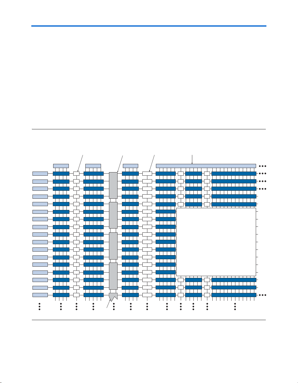
LABs
LABs
LABs
LABs
DSP
Block
M-RAM Block
Each Stratix II device I/O pin is fed by an I/O element (IOE) located at
the end of LAB rows and columns around the periphery of the device.
I/O pins support numerous single-ended and differential I/O standards.
Each IOE contains a bidirectional I/O buffer and six registers for
registering input, output, and output-enable signals. When used with
dedicated clocks, these registers provide exceptional performance and
interface support with external memory devices such as DDR and DDR2
SDRAM, RLDRAM II, and QDR II SRAM devices. High-speed serial
interface channels with dynamic phase alignment (DPA) support data
transfer at up to 1 Gbps using LVDS or HyperTransport
standards.
Figure 2–1 shows an overview of the Stratix II device.
Figure 2–1. Stratix II Block Diagram
TM
technology I/O
2–2 Altera Corporation
Stratix II Device Handbook, Volume 1 May 2007
Page 21
The number of M512 RAM, M4K RAM, and DSP blocks varies by device
along with row and column numbers and M-RAM blocks. Table 2–1 lists
the resources available in Stratix II devices.
Table 2–1. Stratix II Device Resources
Stratix II Architecture
Device
EP2S15 4 / 104 3 / 78 0 2 / 12 30 26
EP2S30 6 / 202 4 / 144 1 2 / 16 49 36
EP2S60 7 / 329 5 / 255 2 3 / 36 62 51
EP2S90 8 / 488 6 / 408 4 3 / 48 71 68
EP2S130 9 / 699 7 / 609 6 3 / 63 81 87
EP2S180 11 / 930 8 / 768 9 4 / 96 100 96
Logic Array Blocks
M512 RAM
Columns/Blocks
Each LAB consists of eight ALMs, carry chains, shared arithmetic chains,
LAB control signals, local interconnect, and register chain connection
lines. The local interconnect transfers signals between ALMs in the same
M4K RAM
Columns/Blocks
M-RAM
Blocks
DSP Block
Columns/Blocks
LAB
Columns
LAB Rows
LAB. Register chain connections transfer the output of an ALM register to
®
the adjacent ALM register in an LAB. The Quartus
II Compiler places
associated logic in an LAB or adjacent LABs, allowing the use of local,
shared arithmetic chain, and register chain connections for performance
and area efficiency. Figure 2–2 shows the Stratix II LAB structure.
Altera Corporation 2–3
May 2007 Stratix II Device Handbook, Volume 1
Page 22
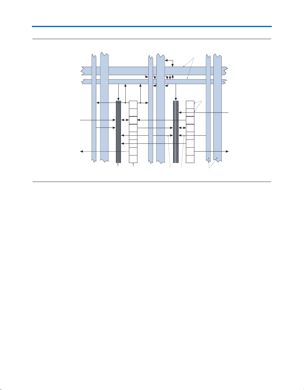
Logic Array Blocks
Direct link
interconnect from
adjacent block
Direct link
interconnect to
adjacent block
Row Interconnects of
Variable Speed & Length
Column Interconnects of
Variable Speed & Length
Local Interconnect is Driven
from Either Side by Columns & LABs,
& from Above by Rows
Local Interconnect
LAB
Direct link
interconnect from
adjacent block
Direct link
interconnect to
adjacent block
ALMs
Figure 2–2. Stratix II LAB Structure
LAB Interconnects
The LAB local interconnect can drive ALMs in the same LAB. It is driven
by column and row interconnects and ALM outputs in the same LAB.
Neighboring LABs, M512 RAM blocks, M4K RAM blocks, M-RAM
blocks, or DSP blocks from the left and right can also drive an LAB's local
interconnect through the direct link connection. The direct link
connection feature minimizes the use of row and column interconnects,
providing higher performance and flexibility. Each ALM can drive
24 ALMs through fast local and direct link interconnects. Figure 2–3
shows the direct link connection.
2–4 Altera Corporation
Stratix II Device Handbook, Volume 1 May 2007
Page 23
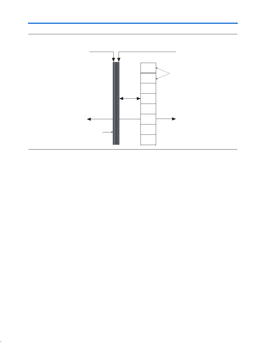
Figure 2–3. Direct Link Connection
ALMs
Direct link
interconnect
to right
Direct link interconnect from
right LAB, TriMatrix memory
block, DSP block, or IOE output
Direct link interconnect from
left LAB, TriMatrix memory
block, DSP block, or IOE output
Local
Interconnect
Direct link
interconnect
to left
LAB Control Signals
Stratix II Architecture
Altera Corporation 2–5
May 2007 Stratix II Device Handbook, Volume 1
Each LAB contains dedicated logic for driving control signals to its ALMs.
The control signals include three clocks, three clock enables, two
asynchronous clears, synchronous clear, asynchronous preset/load, and
synchronous load control signals. This gives a maximum of 11 control
signals at a time. Although synchronous load and clear signals are
generally used when implementing counters, they can also be used with
other functions.
Each LAB can use three clocks and three clock enable signals. However,
there can only be up to two unique clocks per LAB, as shown in the LAB
control signal generation circuit in Figure 2–4. Each LAB's clock and clock
enable signals are linked. For example, any ALM in a particular LAB
using the labclk1 signal also uses labclkena1. If the LAB uses both
the rising and falling edges of a clock, it also uses two LAB-wide clock
signals. De-asserting the clock enable signal turns off the corresponding
LAB-wide clock.
Each LAB can use two asynchronous clear signals and an asynchronous
load/preset signal. By default, the Quartus II software uses a NOT gate
push-back technique to achieve preset. If you disable the NOT gate
push-up option or assign a given register to power up high using the
Quartus II software, the preset is achieved using the asynchronous load
Page 24
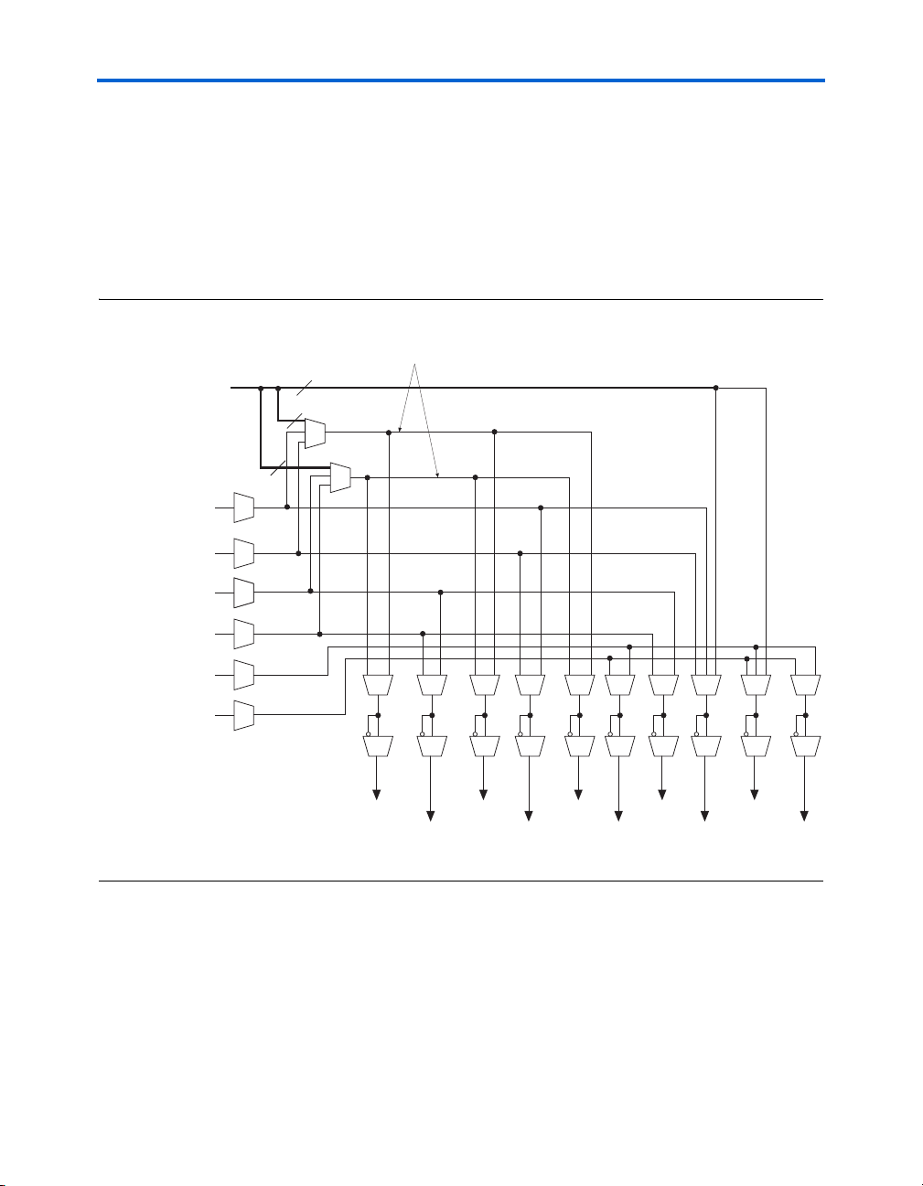
Adaptive Logic Modules
Dedicated Row LAB Clocks
Local Interconnect
Local Interconnect
Local Interconnect
Local Interconnect
Local Interconnect
Local Interconnect
labclk2
syncload
labclkena0
or asyncload
or labpreset
labclk0
labclk1
labclr1
labclkena1 labclkena2 labclr0 synclr
6
6
6
There are two unique
clock signals per LAB.
signal with asynchronous load data input tied high. When the
asynchronous load/preset signal is used, the labclkena0 signal is no
longer available.
Figure 2–4. LAB-Wide Control Signals
The LAB row clocks [5..0] and LAB local interconnect generate the
TM
LAB-wide control signals. The MultiTrack
interconnect's inherent low
skew allows clock and control signal distribution in addition to data.
Figure 2–4 shows the LAB control signal generation circuit.
Adaptive Logic
Modules
The basic building block of logic in the Stratix II architecture, the adaptive
logic module (ALM), provides advanced features with efficient logic
utilization. Each ALM contains a variety of look-up table (LUT)-based
resources that can be divided between two adaptive LUTs (ALUTs). With
up to eight inputs to the two ALUTs, one ALM can implement various
combinations of two functions. This adaptability allows the ALM to be
2–6 Altera Corporation
Stratix II Device Handbook, Volume 1 May 2007
Page 25
completely backward-compatible with four-input LUT architectures. One
DQ
To general or
local routing
reg0
To general or
local routing
datae0
dataf0
shared_arith_in
shared_arith_out
reg_chain_in
reg_chain_out
adder0
dataa
datab
datac
datad
Combinational
Logic
datae1
dataf1
DQ
To general or
local routing
reg1
To general or
local routing
adder1
carry_in
carry_out
ALM can also implement any function of up to six inputs and certain
seven-input functions.
In addition to the adaptive LUT-based resources, each ALM contains two
programmable registers, two dedicated full adders, a carry chain, a
shared arithmetic chain, and a register chain. Through these dedicated
resources, the ALM can efficiently implement various arithmetic
functions and shift registers. Each ALM drives all types of interconnects:
local, row, column, carry chain, shared arithmetic chain, register chain,
and direct link interconnects. Figure 2–5 shows a high-level block
diagram of the Stratix II ALM while Figure 2–6 shows a detailed view of
all the connections in the ALM.
Figure 2–5. High-Level Block Diagram of the Stratix II ALM
Stratix II Architecture
Altera Corporation 2–7
May 2007 Stratix II Device Handbook, Volume 1
Page 26
Adaptive Logic Modules
PRN/ALD
CLRN
D
AD ATA
ENA
Q
PRN/ALD
CLRN
D
AD ATA
ENA
Q
4-Input
LUT
3-Input
LUT
3-Input
LUT
4-Input
LUT
3-Input
LUT
3-Input
LUT
dataa
datac
datae0
dataf0
dataf1
datae1
datab
datad
V
CC
reg_chain_in
sclr asyncload
syncload ena[2..0]
shared_arith_in
carry_in
carry_out clk[2..0]
Local
Interconnect
Row, column &
direct link routing
Row, column &
direct link routing
Local
Interconnect
Row, column &
direct link routing
Row, column &
direct link routing
reg_chain_out
shared_arith_out aclr[1..0]
Local
Interconnect
Local
Interconnect
Local
Interconnect
Local
Interconnect
Local
Interconnect
Local
Interconnect
Local
Interconnect
Local
Interconnect
Figure 2–6. Stratix II ALM Details
2–8 Altera Corporation
Stratix II Device Handbook, Volume 1 May 2007
Page 27

Stratix II Architecture
One ALM contains two programmable registers. Each register has data,
clock, clock enable, synchronous and asynchronous clear, asynchronous
load data, and synchronous and asynchronous load/preset inputs.
Global signals, general-purpose I/O pins, or any internal logic can drive
the register's clock and clear control signals. Either general-purpose I/O
pins or internal logic can drive the clock enable, preset, asynchronous
load, and asynchronous load data. The asynchronous load data input
comes from the datae or dataf input of the ALM, which are the same
inputs that can be used for register packing. For combinational functions,
the register is bypassed and the output of the LUT drives directly to the
outputs of the ALM.
Each ALM has two sets of outputs that drive the local, row, and column
routing resources. The LUT, adder, or register output can drive these
output drivers independently (see Figure 2–6). For each set of output
drivers, two ALM outputs can drive column, row, or direct link routing
connections, and one of these ALM outputs can also drive local
interconnect resources. This allows the LUT or adder to drive one output
while the register drives another output. This feature, called register
packing, improves device utilization because the device can use the
register and the combinational logic for unrelated functions. Another
special packing mode allows the register output to feed back into the LUT
of the same ALM so that the register is packed with its own fan-out LUT.
This provides another mechanism for improved fitting. The ALM can also
drive out registered and unregistered versions of the LUT or adder
output.
f See the Performance & Logic Efficiency Analysis of Stratix II Devices White
Paper for more information on the efficiencies of the Stratix II ALM and
comparisons with previous architectures.
ALM Operating Modes
The Stratix II ALM can operate in one of the following modes:
■ Normal mode
■ Extended LUT mode
■ Arithmetic mode
■ Shared arithmetic mode
Each mode uses ALM resources differently. In each mode, eleven
available inputs to the ALM--the eight data inputs from the LAB local
interconnect; carry-in from the previous ALM or LAB; the shared
arithmetic chain connection from the previous ALM or LAB; and the
register chain connection--are directed to different destinations to
implement the desired logic function. LAB-wide signals provide clock,
asynchronous clear, asynchronous preset/load, synchronous clear,
Altera Corporation 2–9
May 2007 Stratix II Device Handbook, Volume 1
Page 28

Adaptive Logic Modules
synchronous load, and clock enable control for the register. These LABwide signals are available in all ALM modes. See the “LAB Control
Signals” section for more information on the LAB-wide control signals.
The Quartus II software and supported third-party synthesis tools, in
conjunction with parameterized functions such as library of
parameterized modules (LPM) functions, automatically choose the
appropriate mode for common functions such as counters, adders,
subtractors, and arithmetic functions. If required, you can also create
special-purpose functions that specify which ALM operating mode to use
for optimal performance.
Normal Mode
The normal mode is suitable for general logic applications and
combinational functions. In this mode, up to eight data inputs from the
LAB local interconnect are inputs to the combinational logic. The normal
mode allows two functions to be implemented in one Stratix II ALM, or
an ALM to implement a single function of up to six inputs. The ALM can
support certain combinations of completely independent functions and
various combinations of functions which have common inputs.
Figure 2–7 shows the supported LUT combinations in normal mode.
2–10 Altera Corporation
Stratix II Device Handbook, Volume 1 May 2007
Page 29
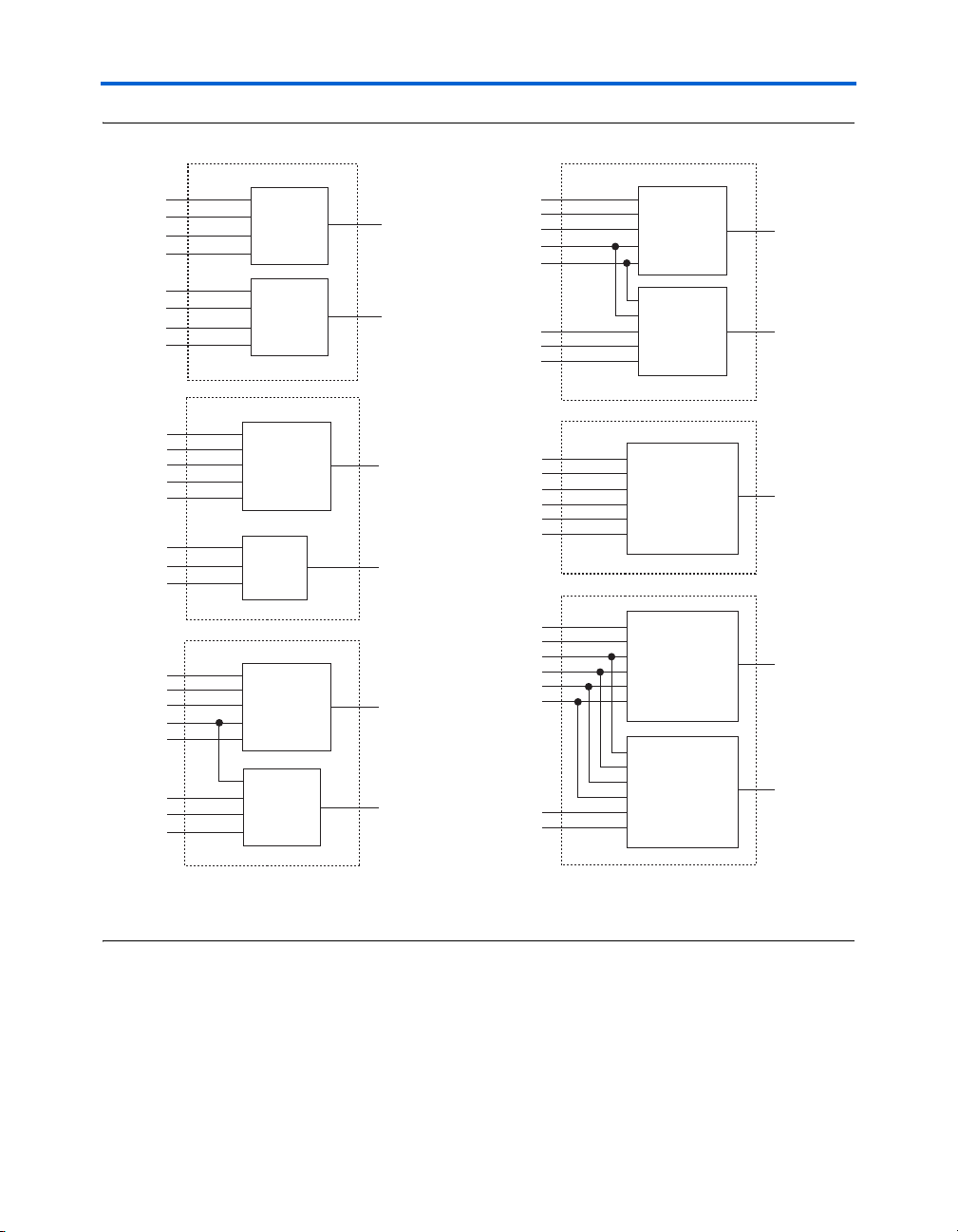
Figure 2–7. ALM in Normal Mode Note (1)
6-Input
LUT
dataf0
datae0
dataf0
datae0
dataa
datab
dataa
datab
datab
datac
datac
dataf0
datae0
dataa
datac
6-Input
LUT
datad
datad
datae1
combout0
combout1
combout0
combout1
combout0
combout1
dataf1
datae1
dataf1
datad
datae1
dataf1
4-Input
LUT
4-Input
LUT
4-Input
LUT
6-Input
LUT
dataf0
datae0
dataa
datab
datac
datad
combout0
5-Input
LUT
5-Input
LUT
dataf0
datae0
dataa
datab
datac
datad
combout0
combout1
datae1
dataf1
5-Input
LUT
dataf0
datae0
dataa
datab
datac
datad
combout0
combout1
datae1
dataf1
5-Input
LUT
3-Input
LUT
Stratix II Architecture
Note to Figure 2–7:
(1) Combinations of functions with fewer inputs than those shown are also supported. For example, combinations of
functions with the following number of inputs are supported: 4 and 3, 3 and 3, 3 and 2, 5 and 2, etc.
The normal mode provides complete backward compatibility with fourinput LUT architectures. Two independent functions of four inputs or less
can be implemented in one Stratix II ALM. In addition, a five-input
function and an independent three-input function can be implemented
without sharing inputs.
Altera Corporation 2–11
May 2007 Stratix II Device Handbook, Volume 1
Page 30
Adaptive Logic Modules
Six-Input
LUT
(Function0)
dataf0
datae0
dataa
datab
datac
Six-Input
LUT
(Function1)
datad
datae1
combout0
combout1
dataf1
inputa
sel0[1..0]
sel1[1..0]
inputb
inputc
inputd
out0
out1
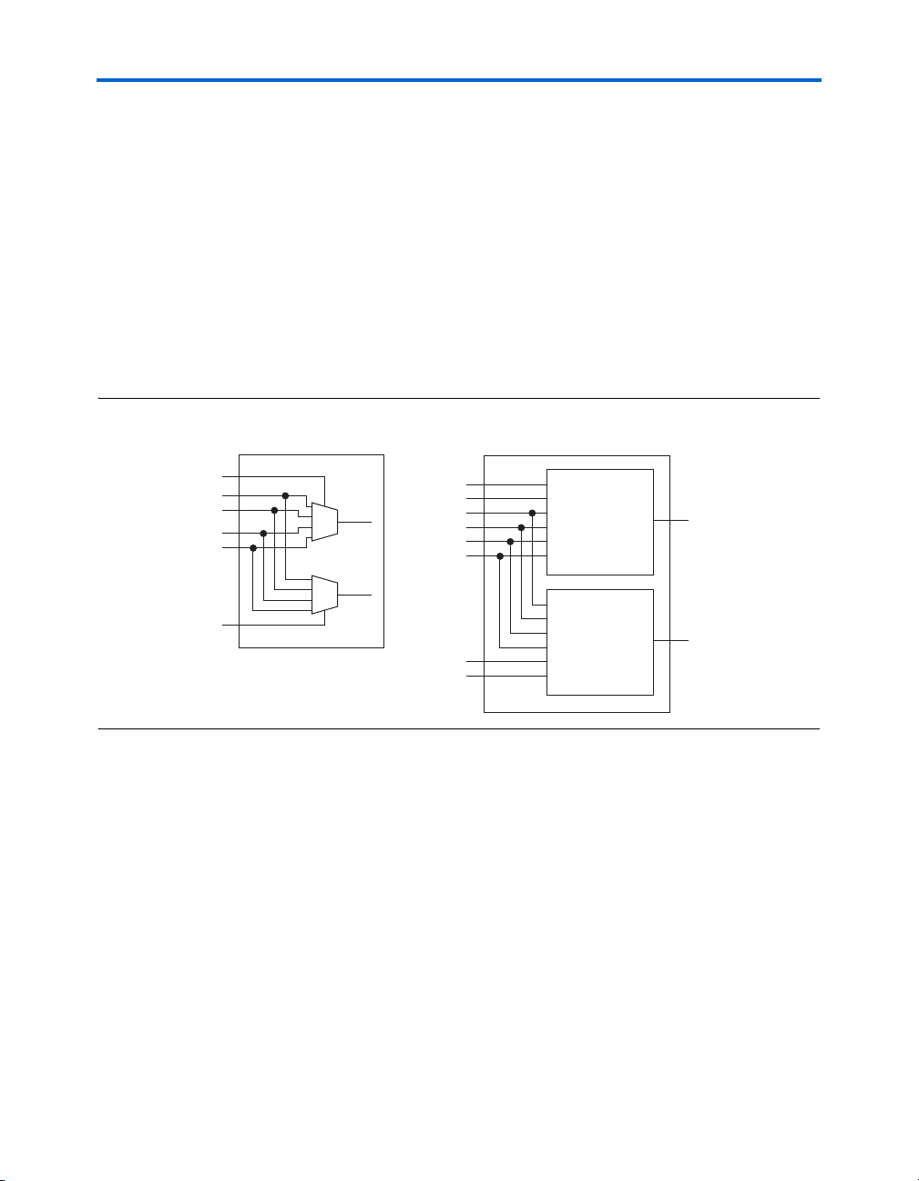
4 × 2 Crossbar Switch Implementation in 1 ALM
For the packing of two five-input functions into one ALM, the functions
must have at least two common inputs. The common inputs are dataa
and datab. The combination of a four-input function with a five-input
function requires one common input (either dataa or datab).
In the case of implementing two six-input functions in one ALM, four
inputs must be shared and the combinational function must be the same.
For example, a 4 × 2 crossbar switch (two 4-to-1 multiplexers with
common inputs and unique select lines) can be implemented in one ALM,
as shown in Figure 2–8. The shared inputs are dataa, datab, datac, and
datad, while the unique select lines are datae0 and dataf0 for
function0, and datae1 and dataf1 for function1. This crossbar
switch consumes four LUTs in a four-input LUT-based architecture.
Figure 2–8. 4 × 2 Crossbar Switch Example
In a sparsely used device, functions that could be placed into one ALM
may be implemented in separate ALMs. The Quartus II Compiler spreads
a design out to achieve the best possible performance. As a device begins
to fill up, the Quartus II software automatically utilizes the full potential
of the Stratix II ALM. The Quartus II Compiler automatically searches for
functions of common inputs or completely independent functions to be
placed into one ALM and to make efficient use of the device resources. In
addition, you can manually control resource usage by setting location
assignments.
Any six-input function can be implemented utilizing inputs dataa,
2–12 Altera Corporation
Stratix II Device Handbook, Volume 1 May 2007
datab, datac, datad, and either datae0 and dataf0 or datae1 and
dataf1. If datae0 and dataf0 are utilized, the output is driven to
register0, and/or register0 is bypassed and the data drives out to
the interconnect using the top set of output drivers (see Figure 2–9). If
Page 31

Stratix II Architecture
6-Input
LUT
dataf0
datae0
dataa
datab
datac
datad
datae1
dataf1
DQ
DQ
To general or
local routing
To general or
local routing
To general or
local routing
reg0
reg1
These inputs are available for register packing.
(2)
datae1 and dataf1 are utilized, the output drives to register1
and/or bypasses register1 and drives to the interconnect using the
bottom set of output drivers. The Quartus II Compiler automatically
selects the inputs to the LUT. Asynchronous load data for the register
comes from the datae or dataf input of the ALM. ALMs in normal
mode support register packing.
Figure 2–9. 6-Input Function in Normal Mode Notes (1), (2)
Notes to Figure 2–9:
(1) If datae1 and dataf1 are used as inputs to the six-input function, then datae0
and dataf0 are available for register packing.
(2) The dataf1 input is available for register packing only if the six-input function is
un-registered.
Altera Corporation 2–13
May 2007 Stratix II Device Handbook, Volume 1
Extended LUT Mode
The extended LUT mode is used to implement a specific set of
seven-input functions. The set must be a 2-to-1 multiplexer fed by two
arbitrary five-input functions sharing four inputs. Figure 2–10 shows the
template of supported seven-input functions utilizing extended LUT
mode. In this mode, if the seven-input function is unregistered, the
unused eighth input is available for register packing.
Functions that fit into the template shown in Figure 2–10 occur naturally
in designs. These functions often appear in designs as “if-else” statements
in Verilog HDL or VHDL code.
Page 32

Adaptive Logic Modules
datae0
combout0
5-Input
LUT
5-Input
LUT
datac
dataa
datab
datad
dataf0
datae1
dataf1
DQ
To general or
local routing
To general or
local routing
reg0
This input is available
for register packing.
(1)
Figure 2–10. Template for Supported Seven-Input Functions in Extended LUT Mode
Note to Figure 2–10:
(1) If the seven-input function is unregistered, the unused eighth input is available for register packing. The second
register, reg1, is not available.
Arithmetic Mode
The arithmetic mode is ideal for implementing adders, counters,
accumulators, wide parity functions, and comparators. An ALM in
arithmetic mode uses two sets of two four-input LUTs along with two
dedicated full adders. The dedicated adders allow the LUTs to be
available to perform pre-adder logic; therefore, each adder can add the
output of two four-input functions. The four LUTs share the dataa and
datab inputs. As shown in Figure 2–11, the carry-in signal feeds to
adder0, and the carry-out from adder0 feeds to carry-in of adder1. The
carry-out from adder1 drives to adder0 of the next ALM in the LAB.
ALMs in arithmetic mode can drive out registered and/or unregistered
versions of the adder outputs.
2–14 Altera Corporation
Stratix II Device Handbook, Volume 1 May 2007
Page 33

Figure 2–11. ALM in Arithmetic Mode
dataf0
datae0
carry_in
carry_out
dataa
datab
datac
datad
datae1
dataf1
DQ
DQ
To general or
local routing
To general or
local routing
reg0
reg1
To general or
local routing
To general or
local routing
4-Input
LUT
4-Input
LUT
4-Input
LUT
4-Input
LUT
adder1
adder0
Stratix II Architecture
While operating in arithmetic mode, the ALM can support simultaneous
use of the adder's carry output along with combinational logic outputs. In
this operation, the adder output is ignored. This usage of the adder with
the combinational logic output provides resource savings of up to 50% for
functions that can use this ability. An example of such functionality is a
conditional operation, such as the one shown in Figure 2–12. The
equation for this example is:
R = (X < Y) ? Y : X
To implement this function, the adder is used to subtract ‘Y’ from ‘X.’ If
‘X’ is less than ‘Y,’ the carry_out signal is ‘1.’ The carry_out signal is
fed to an adder where it drives out to the LAB local interconnect. It then
feeds to the LAB-wide syncload signal. When asserted, syncload
selects the syncdata input. In this case, the data ‘Y’ drives the
syncdata inputs to the registers. If ‘X’ is greater than or equal to ‘Y,’ the
syncload signal is de-asserted and ‘X’ drives the data port of the
registers.
Altera Corporation 2–15
May 2007 Stratix II Device Handbook, Volume 1
Page 34

Adaptive Logic Modules
Y[1]
Y[0]
X[0]
X[0]
carry_out
X[2]
X[2]
X[1]
X[1]
Y[2]
DQ
To general or
local routing
reg0
Comb &
Adder
Logic
Comb &
Adder
Logic
Comb &
Adder
Logic
Comb &
Adder
Logic
DQ
To general or
local routing
reg1
DQ
To general or
local routing
To local routing &
then to LAB-wide
syncload
reg0
syncload
syncload
syncload
ALM 1
ALM 2
R[0]
R[1]
R[2]
Carry Chain
Adder output
is not used.
syncdata
Figure 2–12. Conditional Operation Example
The arithmetic mode also offers clock enable, counter enable,
synchronous up/down control, add/subtract control, synchronous clear,
synchronous load. The LAB local interconnect data inputs generate the
clock enable, counter enable, synchronous up/down and add/subtract
control signals. These control signals are good candidates for the inputs
that are shared between the four LUTs in the ALM. The synchronous clear
and synchronous load options are LAB-wide signals that affect all
registers in the LAB. The Quartus II software automatically places any
registers that are not used by the counter into other LABs.
Carry Chain
The carry chain provides a fast carry function between the dedicated
2–16 Altera Corporation
Stratix II Device Handbook, Volume 1 May 2007
adders in arithmetic or shared arithmetic mode. Carry chains can begin in
either the first ALM or the fifth ALM in an LAB. The final carry-out signal
is routed t o an ALM , wh ere it i s fe d to loc al, row, or col umn int erc onn ect s.
Page 35

Stratix II Architecture
The Quartus II Compiler automatically creates carry chain logic during
design processing, or you can create it manually during design entry.
Parameterized functions such as LPM functions automatically take
advantage of carry chains for the appropriate functions.
The Quartus II Compiler creates carry chains longer than 16 (8 ALMs in
arithmetic or shared arithmetic mode) by linking LABs together
automatically. For enhanced fitting, a long carry chain runs vertically
allowing fast horizontal connections to TriMatrix memory and DSP
blocks. A carry chain can continue as far as a full column.
To avoid routing congestion in one small area of the device when a high
fan-in arithmetic function is implemented, the LAB can support carry
chains that only utilize either the top half or the bottom half of the LAB
before connecting to the next LAB. This leaves the other half of the ALMs
in the LAB available for implementing narrower fan-in functions in
normal mode. Carry chains that use the top four ALMs in the first LAB
carry into the top half of the ALMs in the next LAB within the column.
Carry chains that use the bottom four ALMs in the first LAB carry into the
bottom half of the ALMs in the next LAB within the column. Every other
column of LABs is top-half bypassable, while the other LAB columns are
bottom-half bypassable.
See the “MultiTrack Interconnect” on page 2–22 section for more
information on carry chain interconnect.
Shared Arithmetic Mode
In shared arithmetic mode, the ALM can implement a three-input add. In
this mode, the ALM is configured with four 4-input LUTs. Each LUT
either computes the sum of three inputs or the carry of three inputs. The
output of the carry computation is fed to the next adder (either to adder1
in the same ALM or to adder0 of the next ALM in the LAB) via a
dedicated connection called the shared arithmetic chain. This shared
arithmetic chain can significantly improve the performance of an adder
tree by reducing the number of summation stages required to implement
an adder tree. Figure 2–13 shows the ALM in shared arithmetic mode.
Altera Corporation 2–17
May 2007 Stratix II Device Handbook, Volume 1
Page 36

Adaptive Logic Modules
datae0
carry_in
shared_arith_in
shared_arith_out
carry_out
dataa
datab
datac
datad
datae1
DQ
DQ
To general or
local routing
To general or
local routing
reg0
reg1
To general or
local routing
To general or
local routing
4-Input
LUT
4-Input
LUT
4-Input
LUT
4-Input
LUT
Figure 2–13. ALM in Shared Arithmetic Mode
Note to Figure 2–13:
(1) Inputs dataf0 and dataf1 are available for register packing in shared arithmetic mode.
Adder trees can be found in many different applications. For example, the
summation of the partial products in a logic-based multiplier can be
implemented in a tree structure. Another example is a correlator function
that can use a large adder tree to sum filtered data samples in a given time
2–18 Altera Corporation
Stratix II Device Handbook, Volume 1 May 2007
frame to recover or to de-spread data which was transmitted utilizing
spread spectrum technology.
An example of a three-bit add operation utilizing the shared arithmetic
mode is shown in Figure 2–14. The partial sum (S[2..0]) and the
partial carry (C[2..0]) is obtained using the LUTs, while the result
(R[2..0]) is computed using the dedicated adders.
Page 37

Figure 2–14. Example of a 3-bit Add Utilizing Shared Arithmetic Mode
carry_in = '0'
shared_arith_in = '0'
Z0
Y0
X0
Binary Add
Decimal
Equivalents
+
Z1
X1
R0
C0
S0
S1
S2
C1
C2
'0'
R1
Y1
3-Input
LUT
3-Input
LUT
3-Input
LUT
3-Input
LUT
Z2
Y2
X2
R2
R3
3-Input
LUT
3-Input
LUT
3-Input
LUT
3-Input
LUT
ALM 1
3-Bit Add Example ALM Implementation
ALM 2
X2 X1 X0
Y2 Y1 Y0
Z2 Z1 Z0
S2 S1 S0
C2 C1 C0
R3 R2 R1 R0
+
+
1 1 0
1 0 1
0 1 0
0 0 1
1 1 0
1 1 0 1
+
+
6
5
2
1
2 x 6
13
+
2nd stage add is
implemented in adders.
1st stage add is
implemented in LUTs.
Stratix II Architecture
Shared Arithmetic Chain
In addition to the dedicated carry chain routing, the shared arithmetic
chain available in shared arithmetic mode allows the ALM to implement
a three-input add. This significantly reduces the resources necessary to
implement large adder trees or correlator functions.
The shared arithmetic chains can begin in either the first or fifth ALM in
an LAB. The Quartus II Compiler creates shared arithmetic chains longer
than 16 (8 ALMs in arithmetic or shared arithmetic mode) by linking
LABs together automatically. For enhanced fitting, a long shared
Altera Corporation 2–19
May 2007 Stratix II Device Handbook, Volume 1
Page 38

Adaptive Logic Modules
arithmetic chain runs vertically allowing fast horizontal connections to
TriMatrix memory and DSP blocks. A shared arithmetic chain can
continue as far as a full column.
Similar to the carry chains, the shared arithmetic chains are also top- or
bottom-half bypassable. This capability allows the shared arithmetic
chain to cascade through half of the ALMs in a LAB while leaving the
other half available for narrower fan-in functionality. Every other LAB
column is top-half bypassable, while the other LAB columns are bottomhalf bypassable.
See the “MultiTrack Interconnect” on page 2–22 section for more
information on shared arithmetic chain interconnect.
Register Chain
In addition to the general routing outputs, the ALMs in an LAB have
register chain outputs. The register chain routing allows registers in the
same LAB to be cascaded together. The register chain interconnect allows
an LAB to use LUTs for a single combinational function and the registers
to be used for an unrelated shift register implementation. These resources
speed up connections between ALMs while saving local interconnect
resources (see Figure 2–15). The Quartus II Compiler automatically takes
advantage of these resources to improve utilization and performance.
2–20 Altera Corporation
Stratix II Device Handbook, Volume 1 May 2007
Page 39

Figure 2–15. Register Chain within an LAB Note (1)
DQ
To general or
local routing
reg0
To general or
local routing
reg_chain_in
adder0
DQ
To general or
local routing
reg1
To general or
local routing
adder1
DQ
To general or
local routing
reg0
To general or
local routing
reg_chain_out
adder0
DQ
To general or
local routing
reg1
To general or
local routing
adder1
From Previous ALM
Within The LAB
To Next ALM
within the LAB
Combinational
Logic
Combinational
Logic
Stratix II Architecture
Note to Figure 2–15:
(1) The combinational or adder logic can be utilized to implement an unrelated, un-registered function.
See the “MultiTrack Interconnect” on page 2–22 section for more
information on register chain interconnect.
Altera Corporation 2–21
May 2007 Stratix II Device Handbook, Volume 1
Page 40

MultiTrack Interconnect
Clear & Preset Logic Control
LAB-wide signals control the logic for the register's clear and load/preset
signals. The ALM directly supports an asynchronous clear and preset
function. The register preset is achieved through the asynchronous load
of a logic high. The direct asynchronous preset does not require a NOTgate push-back technique. Stratix II devices support simultaneous
asynchronous load/preset, and clear signals. An asynchronous clear
signal takes precedence if both signals are asserted simultaneously. Each
LAB supports up to two clears and one load/preset signal.
In addition to the clear and load/preset ports, Stratix II devices provide a
device-wide reset pin (DEV_CLRn) that resets all registers in the device.
An option set before compilation in the Quartus II software controls this
pin. This device-wide reset overrides all other control signals.
MultiTrack
Interconnect
In the Stratix II architecture, connections between ALMs, TriMatrix
memory, DSP blocks, and device I/O pins are provided by the MultiTrack
interconnect structure with DirectDrive
interconnect consists of continuous, performance-optimized routing lines
of different lengths and speeds used for inter- and intra-design block
connectivity. The Quartus II Compiler automatically places critical design
paths on faster interconnects to improve design performance.
DirectDrive technology is a deterministic routing technology that ensures
identical routing resource usage for any function regardless of placement
in the device. The MultiTrack interconnect and DirectDrive technology
simplify the integration stage of block-based designing by eliminating the
re-optimization cycles that typically follow design changes and
additions.
The MultiTrack interconnect consists of row and column interconnects
that span fixed distances. A routing structure with fixed length resources
for all devices allows predictable and repeatable performance when
migrating through different device densities. Dedicated row
interconnects route signals to and from LABs, DSP blocks, and TriMatrix
memory in the same row. These row resources include:
■ Direct link interconnects between LABs and adjacent blocks
■ R4 interconnects traversing four blocks to the right or left
■ R24 row interconnects for high-speed access across the length of the
device
TM
technology. The MultiTrack
2–22 Altera Corporation
Stratix II Device Handbook, Volume 1 May 2007
Page 41

Stratix II Architecture
Primary
LAB (2)
R4 Interconnect
Driving Left
Adjacent LAB can
Drive onto Another
LAB's R4 Interconnect
C4 and C16
Column Interconnects (1)
R4 Interconnect
Driving Right
LAB
Neighbor
LAB
Neighbor
The direct link interconnect allows an LAB, DSP block, or TriMatrix
memory block to drive into the local interconnect of its left and right
neighbors and then back into itself. This provides fast communication
between adjacent LABs and/or blocks without using row interconnect
resources.
The R4 interconnects span four LABs, three LABs and one M512 RAM
block, two LABs and one M4K RAM block, or two LABs and one DSP
block to the right or left of a source LAB. These resources are used for fast
row connections in a four-LAB region. Every LAB has its own set of R4
interconnects to drive either left or right. Figure 2–16 shows R4
interconnect connections from an LAB. R4 interconnects can drive and be
driven by DSP blocks and RAM blocks and row IOEs. For LAB
interfacing, a primary LAB or LAB neighbor can drive a given R4
interconnect. For R4 interconnects that drive to the right, the primary
LAB and right neighbor can drive on to the interconnect. For R4
interconnects that drive to the left, the primary LAB and its left neighbor
can drive on to the interconnect. R4 interconnects can drive other R4
interconnects to extend the range of LABs they can drive. R4
interconnects can also drive C4 and C16 interconnects for connections
from one row to another. Additionally, R4 interconnects can drive R24
interconnects.
Figure 2–16. R4 Interconnect Connections Notes (1), (2), (3)
Notes to Figure 2–16:
(1) C4 and C16 interconnects can drive R4 interconnects.
(2) This pattern is repeated for every LAB in the LAB row.
(3) The LABs in Figure 2–16 show the 16 possible logical outputs per LAB.
Altera Corporation 2–23
May 2007 Stratix II Device Handbook, Volume 1
Page 42

MultiTrack Interconnect
R24 row interconnects span 24 LABs and provide the fastest resource for
long row connections between LABs, TriMatrix memory, DSP blocks, and
Row IOEs. The R24 row interconnects can cross M-RAM blocks. R24 row
interconnects drive to other row or column interconnects at every fourth
LAB and do not drive directly to LAB local interconnects. R24 row
interconnects drive LAB local interconnects via R4 and C4 interconnects.
R24 interconnects can drive R24, R4, C16, and C4 interconnects.
The column interconnect operates similarly to the row interconnect and
vertically routes signals to and from LABs, TriMatrix memory, DSP
blocks, and IOEs. Each column of LABs is served by a dedicated column
interconnect. These column resources include:
■ Shared arithmetic chain interconnects in an LAB
■ Carry chain interconnects in an LAB and from LAB to LAB
■ Register chain interconnects in an LAB
■ C4 interconnects traversing a distance of four blocks in up and down
direction
■ C16 column interconnects for high-speed vertical routing through
the device
Stratix II devices include an enhanced interconnect structure in LABs for
routing shared arithmetic chains and carry chains for efficient arithmetic
functions. The register chain connection allows the register output of one
ALM to connect directly to the register input of the next ALM in the LAB
for fast shift registers. These ALM to ALM connections bypass the local
interconnect. The Quartus II Compiler automatically takes advantage of
these resources to improve utilization and performance. Figure 2–17
shows the shared arithmetic chain, carry chain and register chain
interconnects.
2–24 Altera Corporation
Stratix II Device Handbook, Volume 1 May 2007
Page 43

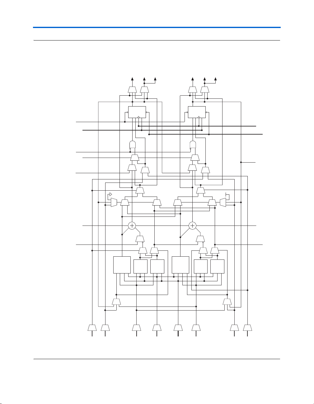
Stratix II Architecture
ALM 1
ALM 2
ALM 3
ALM 4
ALM 5
ALM 6
ALM 8
ALM 7
Carry Chain & Shared
Arithmetic Chain
Local
Interconnect
Register Chain
Routing to Adjacent
ALM's Register Inpu
Local Interconnect
Routing Among ALMs
in the LAB
Figure 2–17. Shared Arithmetic Chain, Carry Chain & Register Chain
Interconnects
Altera Corporation 2–25
May 2007 Stratix II Device Handbook, Volume 1
The C4 interconnects span four LABs, M512, or M4K blocks up or down
from a source LAB. Every LAB has its own set of C4 interconnects to drive
either up or down. Figure 2–18 shows the C4 interconnect connections
from an LAB in a column. The C4 interconnects can drive and be driven
by all types of architecture blocks, including DSP blocks, TriMatrix
memory blocks, and column and row IOEs. For LAB interconnection, a
primary LAB or its LAB neighbor can drive a given C4 interconnect. C4
interconnects can drive each other to extend their range as well as drive
row interconnects for column-to-column connections.
Page 44

MultiTrack Interconnect
C4 Interconnect
Drives Local and R4
Interconnects
up to Four Rows
Adjacent LAB can
drive onto neighboring
LAB's C4 interconnect
C4 Interconnect
Driving Up
C4 Interconnect
Driving Down
LAB
Row
Interconnect
Local
Interconnect
Figure 2–18. C4 Interconnect Connections Note (1)
Note to Figure 2–18:
(1) Each C4 interconnect can drive either up or down four rows.
2–26 Altera Corporation
Stratix II Device Handbook, Volume 1 May 2007
Page 45

C16 column interconnects span a length of 16 LABs and provide the
fastest resource for long column connections between LABs, TriMatrix
memory blocks, DSP blocks, and IOEs. C16 interconnects can cross
M-RAM blocks and also drive to row and column interconnects at every
fourth LAB. C16 interconnects drive LAB local interconnects via C4 and
R4 interconnects and do not drive LAB local interconnects directly.
All embedded blocks communicate with the logic array similar to LABto-LAB interfaces. Each block (that is, TriMatrix memory and DSP blocks)
connects to row and column interconnects and has local interconnect
regions driven by row and column interconnects. These blocks also have
direct link interconnects for fast connections to and from a neighboring
LAB. All blocks are fed by the row LAB clocks, labclk[5..0].
Table 2–2 shows the Stratix II device’s routing scheme.
Table 2–2. Stratix II Device Routing Scheme (Part 1 of 2)
Source
Carry Chain
Register Chain
Local Interconnect
Direct Link Interconnect
v
v vvvv
vvvv
vvv
vvvv
vvv v
vvv v
vvvv
vv v
Shared arithmetic chain
Carry chain
Register chain
Local interconnect
Direct link interconnect
R4 interconnect
R24 interconnect
C4 interconnect
C16 interconnect
ALM
M512 RAM block
M4K RAM block
M-RAM block
DSP blocks
Shared Arithmetic Chain
vvvvvv v
Destination
R24 Interconnect
C4 Interconnect
R4 Interconnect
Stratix II Architecture
ALM
DSP Blocks
C16 Interconnect
M-RAM Block
M4K RAM Block
M512 RAM Block
Column IOE
v
v
v
vvvvvvv
Row IOE
Altera Corporation 2–27
May 2007 Stratix II Device Handbook, Volume 1
Page 46

Tri M a t r ix Memo r y
Table 2–2. Stratix II Device Routing Scheme (Part 2 of 2)
Source
Carry Chain
Register Chain
Local Interconnect
Shared Arithmetic Chain
Column IOE
Row IOE
Direct Link Interconnect
vvv
vvvv
R4 Interconnect
Destination
C4 Interconnect
R24 Interconnect
ALM
C16 Interconnect
M512 RAM Block
DSP Blocks
M-RAM Block
M4K RAM Block
Row IOE
Column IOE
TriMatrix
Memory
TriMatrix memory consists of three types of RAM blocks: M512, M4K,
and M-RAM. Although these memory blocks are different, they can all
implement various types of memory with or without parity, including
true dual-port, simple dual-port, and single-port RAM, ROM, and FIFO
buffers. Table 2–3 shows the size and features of the different RAM
blocks.
Table 2–3. TriMatrix Memory Features (Part 1 of 2)
Memory Feature
Maximum performance 500 MHz 550 MHz 420 MHz
True dual-port memory
Simple dual-port memory
Single-port memory
Shift register
ROM
FIFO buffer
Pack mode
Byte enable
Address clock enable
Parity bits
Mixed clock mode
Memory initialization (.mif)
M512 RAM Block
(32 × 18 Bits)
vvv
vvv
vv
vv
vvv
vvv
vvv
vvv
vv
M4K RAM Block
(128 × 36 Bits)
M-RAM Block
(4K × 144 Bits)
vv
(1)
vv
vv
2–28 Altera Corporation
Stratix II Device Handbook, Volume 1 May 2007
Page 47

Table 2–3. TriMatrix Memory Features (Part 2 of 2)
Stratix II Architecture
Memory Feature
Simple dual-port memory
mixed width support
True dual-port memory
mixed width support
Power-up conditions Outputs cleared Outputs cleared Outputs unknown
Register clears Output registers Output registers Output registers
Mixed-port read-during-write Unknown output/old data Unknown output/old data Unknown output
Configurations 512 × 1
Notes to Ta b l e 2 – 3:
(1) The M-RAM block does not support memory initializations. However, the M-RAM block can emulate a ROM
function using a dual-port RAM bock. The Stratix II device must write to the dual-port memory once and then
disable the write-enable ports afterwards.
M512 RAM Block
(32 × 18 Bits)
vvv
256 × 2
128 × 4
64 × 8
64 × 9
32 × 16
32 × 18
M4K RAM Block
(128 × 36 Bits)
4K × 1
2K × 2
1K × 4
512 × 8
512 × 9
256 × 16
256 × 18
128 × 32
128 × 36
M-RAM Block
(4K × 144 Bits)
vv
64K × 8
64K × 9
32K × 16
32K × 18
16K × 32
16K × 36
8K × 64
8K × 72
4K × 128
4K × 144
Memory Block Size
TriMatrix memory provides three different memory sizes for efficient
application support. The Quartus II software automatically partitions the
user-defined memory into the embedded memory blocks using the most
efficient size combinations. You can also manually assign the memory to
a specific block size or a mixture of block sizes.
When applied to input registers, the asynchronous clear signal for the
TriMatrix embedded memory immediately clears the input registers.
However, the output of the memory block does not show the effects until
the next clock edge. When applied to output registers, the asynchronous
clear signal clears the output registers and the effects are seen
immediately.
Altera Corporation 2–29
May 2007 Stratix II Device Handbook, Volume 1
Page 48

Tri M a t r ix Memo r y
M512 RAM Block
The M512 RAM block is a simple dual-port memory block and is useful
for implementing small FIFO buffers, DSP, and clock domain transfer
applications. Each block contains 576 RAM bits (including parity bits).
M512 RAM blocks can be configured in the following modes:
■ Simple dual-port RAM
■ Single-port RAM
■ FIFO
■ ROM
■ Shift register
1 Violating the setup or hold time on the memory block address
registers could corrupt memory contents. This applies to both
read and write operations.
When configured as RAM or ROM, you can use an initialization file to
pre-load the memory contents.
M512 RAM blocks can have different clocks on its inputs and outputs.
The wren, datain, and write address registers are all clocked together
from one of the two clocks feeding the block. The read address, rden, and
output registers can be clocked by either of the two clocks driving the
block. This allows the RAM block to operate in read/write or
input/output clock modes. Only the output register can be bypassed. The
six labclk signals or local interconnect can drive the inclock,
outclock, wren, rden, and outclr signals. Because of the advanced
interconnect between the LAB and M512 RAM blocks, ALMs can also
control the wren and rden signals and the RAM clock, clock enable, and
asynchronous clear signals. Figure 2–19 shows the M512 RAM block
control signal generation logic.
The RAM blocks in Stratix II devices have local interconnects to allow
ALMs and interconnects to drive into RAM blocks. The M512 RAM block
local interconnect is driven by the R4, C4, and direct link interconnects
from adjacent LABs. The M512 RAM blocks can communicate with LABs
on either the left or right side through these row interconnects or with
LAB columns on the left or right side with the column interconnects. The
M512 RAM block has up to 16 direct link input connections from the left
adjacent LABs and another 16 from the right adjacent LAB. M512 RAM
outputs can also connect to left and right LABs through direct link
interconnect. The M512 RAM block has equal opportunity for access and
performance to and from LABs on either its left or right side. Figure 2–20
shows the M512 RAM block to logic array interface.
2–30 Altera Corporation
Stratix II Device Handbook, Volume 1 May 2007
Page 49

Figure 2–19. M512 RAM Block Control Signals
inclocken
outclockinclock
outclocken
rden
wren
Dedicated
Row LAB
Clocks
Local
Interconnect
Local
Interconnect
Local
Interconnect
Local
Interconnect
Local
Interconnect
Local
Interconnect
outclr
6
Local
Interconnect
Local
Interconnect
Stratix II Architecture
Altera Corporation 2–31
May 2007 Stratix II Device Handbook, Volume 1
Page 50

Tri M a t r ix Memo r y
dataout
M512 RAM
Block
datain
clocks
16
Direct link
interconnect
from adjacent LAB
Direct link
interconnect
to adjacent LAB
Direct link
interconnect
from adjacent LAB
Direct link
interconnect
to adjacent LAB
M512 RAM Block Local
Interconnect Region
C4 Interconnect
R4 Interconnect
control
signals
address
LAB Row Clocks
2
6
Figure 2–20. M512 RAM Block LAB Row Interface
M4K RAM Blocks
The M4K RAM block includes support for true dual-port RAM. The M4K
RAM block is used to implement buffers for a wide variety of applications
such as storing processor code, implementing lookup schemes, and
implementing larger memory applications. Each block contains 4,608
RAM bits (including parity bits). M4K RAM blocks can be configured in
the following modes:
■ True dual-port RAM
■ Simple dual-port RAM
■ Single-port RAM
■ FIFO
■ ROM
■ Shift register
When configured as RAM or ROM, you can use an initialization file to
pre-load the memory contents.
2–32 Altera Corporation
Stratix II Device Handbook, Volume 1 May 2007
Page 51

The M4K RAM blocks allow for different clocks on their inputs and
clock_b
clocken_aclock_a
clocken_b
aclr_b
aclr_a
Dedicated
Row LAB
Clocks
Local
Interconnect
Local
Interconnect
Local
Interconnect
Local
Interconnect
Local
Interconnect
Local
Interconnect
Local
Interconnect
Local
Interconnect
renwe_b
renwe_a
6
outputs. Either of the two clocks feeding the block can clock M4K RAM
block registers (renwe, address, byte enable, datain, and output registers).
Only the output register can be bypassed. The six labclk signals or local
interconnects can drive the control signals for the A and B ports of the
M4K RAM block. ALMs can also control the clock_a, clock_b,
renwe_a, renwe_b, clr_a, clr_b, clocken_a, and clocken_b
signals, as shown in Figure 2–21.
The R4, C4, and direct link interconnects from adjacent LABs drive the
M4K RAM block local interconnect. The M4K RAM blocks can
communicate with LABs on either the left or right side through these row
resources or with LAB columns on either the right or left with the column
resources. Up to 16 direct link input connections to the M4K RAM Block
are possible from the left adjacent LABs and another 16 possible from the
right adjacent LAB. M4K RAM block outputs can also connect to left and
right LABs through direct link interconnect. Figure 2–22 shows the M4K
RAM block to logic array interface.
Figure 2–21. M4K RAM Block Control Signals
Stratix II Architecture
Altera Corporation 2–33
May 2007 Stratix II Device Handbook, Volume 1
Page 52

Tri M a t r ix Memo r y
dataout
M4K RAM
Block
datain
address
16
36
Direct link
interconnect
from adjacent LAB
Direct link
interconnect
to adjacent LAB
Direct link
interconnect
from adjacent LAB
Direct link
interconnect
to adjacent LAB
M4K RAM Block Local
Interconnect Region
C4 Interconnect
R4 Interconnect
LAB Row Clocks
clocks
byte
enable
control
signals
6
Figure 2–22. M4K RAM Block LAB Row Interface
M-RAM Block
The largest TriMatrix memory block, the M-RAM block, is useful for
applications where a large volume of data must be stored on-chip. Each
block contains 589,824 RAM bits (including parity bits). The M-RAM
block can be configured in the following modes:
■ True dual-port RAM
■ Simple dual-port RAM
■ Single-port RAM
■ FIFO
You cannot use an initialization file to initialize the contents of an M-RAM
block. All M-RAM block contents power up to an undefined value. Only
synchronous operation is supported in the M-RAM block, so all inputs
are registered. Output registers can be bypassed.
2–34 Altera Corporation
Stratix II Device Handbook, Volume 1 May 2007
Page 53

Similar to all RAM blocks, M-RAM blocks can have different clocks on
clock_a
clock_b
clocken_a
clocken_b
aclr_a
aclr_b
Dedicated
Row LAB
Clocks
Local
Interconnect
Local
Interconnect
Local
Interconnect
Local
Interconnect
renwe_a
renwe_b
6
Local
Interconnect
Local
Interconnect
Local
Interconnect
Local
Interconnect
Local
Interconnect
Local
Interconnect
Local
Interconnect
Local
Interconnect
their inputs and outputs. Either of the two clocks feeding the block can
clock M-RAM block registers (renwe, address, byte enable, datain, and
output registers). The output register can be bypassed. The six labclk
signals or local interconnect can drive the control signals for the A and B
ports of the M-RAM block. ALMs can also control the clock_a,
clock_b, renwe_a, renwe_b, clr_a, clr_b, clocken_a, and
clocken_b signals as shown in Figure 2–23.
Figure 2–23. M-RAM Block Control Signals
Stratix II Architecture
The R4, R24, C4, and direct link interconnects from adjacent LABs on
either the right or left side drive the M-RAM block local interconnect. Up
to 16 direct link input connections to the M-RAM block are possible from
the left adjacent LABs and another 16 possible from the right adjacent
LAB. M-RAM block outputs can also connect to left and right LABs
through direct link interconnect. Figure 2–24 shows an example floorplan
for the EP2S130 device and the location of the M-RAM interfaces.
Figures 2–25 and 2–26 show the interface between the M-RAM block and
the logic array.
Altera Corporation 2–35
May 2007 Stratix II Device Handbook, Volume 1
Page 54

Tri M a t r ix Memo r y
DSP
Blocks
DSP
Blocks
M4K
Blocks
M512
Blocks
LABs
M-RAM
Block
M-RAM
Block
M-RAM
Block
M-RAM
Block
M-RAM
Block
M-RAM
Block
M-RAM blocks interface to
LABs on right and left sides for
easy access to horizontal I/O pins
Figure 2–24. EP2S130 Device with M-RAM Interface Locations Note (1)
Note to Figure 2–24:
(1) The device shown is an EP2S130 device. The number and position of M-RAM blocks varies in other devices.
2–36 Altera Corporation
Stratix II Device Handbook, Volume 1 May 2007
Page 55

Figure 2–25. M-RAM Block LAB Row Interface Note (1)
M-RAM Block
Port BPort A
Row Unit Interface Allows LAB
Rows to Drive Port B Datain,
Dataout, Address and Control
Signals to and from M-RAM Block
Row Unit Interface Allows LAB
Rows to Drive Port A Datain,
Dataout, Address and Control
Signals to and from M-RAM Block
LABs in Row
M-RAM Boundary
LABs in Row
M-RAM Boundary
LAB Interface
Blocks
L0
L1
L2
L3
L4
L5
R0
R1
R2
R3
R4
R5
Stratix II Architecture
Note to Figure 2–25:
(1) Only R24 and C16 interconnects cross the M-RAM block boundaries.
Altera Corporation 2–37
May 2007 Stratix II Device Handbook, Volume 1
Page 56

Tri M a t r ix Memo r y
LAB
Row Interface Block
M-RAM Block
16
Up to 28
datain_a[ ]
addressa[ ]
addr_ena_a
renwe_a
byteenaA[ ]
clocken_a
clock_a
aclr_a
M-RAM Block to
LAB Row Interface
Block Interconnect Region
R4 and R24 InterconnectsC4 Interconnect
Direct Link
Interconnects
dataout_a[ ]
Up to 16
Figure 2–26. M-RAM Row Unit Interface to Interconnect
Table 2–4 shows the input and output data signal connections along with
the address and control signal input connections to the row unit interfaces
(L0 to L5 and R0 to R5).
2–38 Altera Corporation
Stratix II Device Handbook, Volume 1 May 2007
Page 57

Stratix II Architecture
Table 2–4. M-RAM Row Interface Unit Signals
Unit Interface Block Input Signals Output Signals
L0 datain_a[14..0]
byteena_a[1..0]
L1 datain_a[29..15]
byteena_a[3..2]
L2 datain_a[35..30]
addressa[4..0]
addr_ena_a
clock_a
clocken_a
renwe_a
aclr_a
L3 addressa[15..5]
datain_a[41..36]
L4 datain_a[56..42]
byteena_a[5..4]
L5 datain_a[71..57]
byteena_a[7..6]
R0 datain_b[14..0]
byteena_b[1..0]
R1 datain_b[29..15]
byteena_b[3..2]
R2 datain_b[35..30]
addressb[4..0]
addr_ena_b
clock_b
clocken_b
renwe_b
aclr_b
R3 addressb[15..5]
datain_b[41..36]
R4 datain_b[56..42]
byteena_b[5..4]
R5 datain_b[71..57]
byteena_b[7..6]
dataout_a[11..0]
dataout_a[23..12]
dataout_a[35..24]
dataout_a[47..36]
dataout_a[59..48]
dataout_a[71..60]
dataout_b[11..0]
dataout_b[23..12]
dataout_b[35..24]
dataout_b[47..36]
dataout_b[59..48]
dataout_b[71..60]
f See the TriMatrix Embedded Memory Blocks in Stratix II & Stratix II GX
Devices chapter in volume 2 of the Stratix II Device Handbook or the
Stratix II GX Device Handbook for more information on TriMatrix
memory.
Altera Corporation 2–39
May 2007 Stratix II Device Handbook, Volume 1
Page 58

Digital Signal Processing Block
Digital Signal
Processing
Block
The most commonly used DSP functions are FIR filters, complex FIR
filters, IIR filters, fast Fourier transform (FFT) functions, direct cosine
transform (DCT) functions, and correlators. All of these use the multiplier
as the fundamental building block. Additionally, some applications need
specialized operations such as multiply-add and multiply-accumulate
operations. Stratix II devices provide DSP blocks to meet the arithmetic
requirements of these functions.
Each Stratix II device has from two to four columns of DSP blocks to
efficiently implement DSP functions faster than ALM-based
implementations. Stratix II devices have up to 24 DSP blocks per column
(see Table 2–5). Each DSP block can be configured to support up to:
■ Eight 9 × 9-bit multipliers
■ Four 18 × 18-bit multipliers
■ One 36 × 36-bit multiplier
As indicated, the Stratix II DSP block can support one 36 × 36-bit
multiplier in a single DSP block. This is true for any combination of
signed, unsigned, or mixed sign multiplications.
1 This list only shows functions that can fit into a single DSP block.
Multiple DSP blocks can support larger multiplication
functions.
2–40 Altera Corporation
Stratix II Device Handbook, Volume 1 May 2007
Page 59

Stratix II Architecture
DSP Block
Column
4 LAB
Rows
DSP Block
Figure 2–27 shows one of the columns with surrounding LAB rows.
Figure 2–27. DSP Blocks Arranged in Columns
Altera Corporation 2–41
May 2007 Stratix II Device Handbook, Volume 1
Page 60

Digital Signal Processing Block
Table 2–5 shows the number of DSP blocks in each Stratix II device.
Table 2–5. DSP Blocks in Stratix II Devices Note (1)
Device DSP Blocks
EP2S15 12 96 48 12
EP2S30 16 128 64 16
EP2S60 36 288 144 36
EP2S90 48 384 192 48
EP2S130 63 504 252 63
EP2S180 96 768 384 96
Note to Ta b l e 2 – 5:
(1) Each device has either the numbers of 9 × 9-, 18 × 18-, or 36 × 36-bit multipliers
shown. The total number of multipliers for each device is not the sum of all the
multipliers.
Total 9 × 9
Multipliers
Total 18 × 18
Multipliers
Total 36 × 36
Multipliers
DSP block multipliers can optionally feed an adder/subtractor or
accumulator in the block depending on the configuration. This makes
routing to ALMs easier, saves ALM routing resources, and increases
performance, because all connections and blocks are in the DSP block.
Additionally, the DSP block input registers can efficiently implement shift
registers for FIR filter applications, and DSP blocks support Q1.15 format
rounding and saturation.
Figure 2–28 shows the top-level diagram of the DSP block configured for
18 × 18-bit multiplier mode.
2–42 Altera Corporation
Stratix II Device Handbook, Volume 1 May 2007
Page 61

Figure 2–28. DSP Block Diagram for 18 × 18-Bit Configuration
Adder/
Subtractor/
Accumulator
1
Adder
Multiplier Block
PRN
CLRN
DQ
ENA
PRN
CLRN
DQ
ENA
PRN
CLRN
DQ
ENA
PRN
CLRN
DQ
ENA
PRN
CLRN
DQ
ENA
PRN
CLRN
DQ
ENA
PRN
CLRN
DQ
ENA
PRN
CLRN
DQ
ENA
PRN
CLRN
DQ
ENA
PRN
CLRN
DQ
ENA
PRN
CLRN
DQ
ENA
PRN
CLRN
DQ
ENA
Summation
Block
Adder Output Block
Adder/
Subtractor/
Accumulator
2
Q1.15
Round/
Saturate
Q1.15
Round/
Saturate
Q1.15
Round/
Saturate
Q1.15
Round/
Saturate
to MultiTrack
Interconnect
CLRN
DQ
ENA
From the row
interface block
Optional Serial Shift
Register Inputs from
Previous DSP Block
Optional Serial Shift
Register Outputs to
Next DSP Block
in the Column
Optional Input Register
Stage with Parallel Input or
Shift Register Configuration
Optional Pipline
Register Stage
Summation Stage
for Adding Four
Multipliers Together
Optional Stage Configurable
as Accumulator or Dynamic
Adder/Subtractor
Output
Selection
Multiplexer
Q1.15
Round/
Saturate
Q1.15
Round/
Saturate
Stratix II Architecture
Altera Corporation 2–43
May 2007 Stratix II Device Handbook, Volume 1
Page 62

Digital Signal Processing Block
Modes of Operation
The adder, subtractor, and accumulate functions of a DSP block have four
modes of operation:
■ Simple multiplier
■ Multiply-accumulator
■ Two-multipliers adder
■ Four-multipliers adder
Table 2–6 shows the different number of multipliers possible in each DSP
block mode according to size. These modes allow the DSP blocks to
implement numerous applications for DSP including FFTs, complex FIR,
FIR, and 2D FIR filters, equalizers, IIR, correlators, matrix multiplication
and many other functions. The DSP blocks also support mixed modes
and mixed multiplier sizes in the same block. For example, half of one
DSP block can implement one 18 × 18-bit multiplier in multiplyaccumulator mode, while the other half of the DSP block implements four
9 × 9-bit multipliers in simple multiplier mode.
Table 2–6. Multiplier Size & Configurations per DSP Block
DSP Block Mode 9 × 9 18 × 18 36 × 36
Multiplier Eight multipliers with
eight product outputs
Multiply-accumulator - Two 52-bit multiply-
Two-multipliers adder Four two-multiplier adder
(two 9 × 9 complex
multiply)
Four-multipliers adder Two four-multiplier adder One four-multiplier adder -
Four multipliers with four
product outputs
accumulate blocks
Two two-multiplier adder
(one 18 × 18 complex
multiply)
One multiplier with one
product output
-
-
DSP Block Interface
Stratix II device DSP block input registers can generate a shift register that
can cascade down in the same DSP block column. Dedicated connections
between DSP blocks provide fast connections between the shift register
inputs to cascade the shift register chains. You can cascade registers
within multiple DSP blocks for 9 × 9- or 18 × 18-bit FIR filters larger than
four taps, with additional adder stages implemented in ALMs. If the DSP
block is configured as 36 × 36 bits, the adder, subtractor, or accumulator
stages are implemented in ALMs. Each DSP block can route the shift
register chain out of the block to cascade multiple columns of DSP blocks.
2–44 Altera Corporation
Stratix II Device Handbook, Volume 1 May 2007
Page 63

A1[17..0]
B1[17..0]
A2[17..0]
B2[17..0]
A3[17..0]
B3[17..0]
A4[17..0]
B4[17..0]
OA[17..0]
OB[17..0]
OC[17..0]
OD[17..0]
OE[17..0]
OF[17..0]
OG[17..0]
OH[17..0]
DSP Block
R4, C4 & Direct
Link Interconnects
R4, C4 & Direct
Link Interconnects
Stratix II Architecture
The DSP block is divided into four block units that interface with four
LAB rows on the left and right. Each block unit can be considered one
complete 18 × 18-bit multiplier with 36 inputs and 36 outputs. A local
interconnect region is associated with each DSP block. Like an LAB, this
interconnect region can be fed with 16 direct link interconnects from the
LAB to the left or right of the DSP block in the same row. R4 and C4
routing resources can access the DSP block's local interconnect region.
The outputs also work similarly to LAB outputs as well. Eighteen outputs
from the DSP block can drive to the left LAB through direct link
interconnects and eighteen can drive to the right LAB though direct link
interconnects. All 36 outputs can drive to R4 and C4 routing
interconnects. Outputs can drive right- or left-column routing.
Figures 2–29 and 2–30 show the DSP block interfaces to LAB rows.
Figure 2–29. DSP Block Interconnect Interface
Altera Corporation 2–45
May 2007 Stratix II Device Handbook, Volume 1
Page 64

Digital Signal Processing Block
LAB LAB
Row Interface
Block
DSP Block
Row Structure
16
OA[17..0]
OB[17..0]
A[17..0]
B[17..0]
DSP Block to
LAB Row Interface
Block Interconnect Region
36 Inputs per Row 36 Outputs per Row
R4 Interconnect
C4 Interconnect
Direct Link Interconnect
from Adjacent LAB
Direct Link Outputs
to Adjacent LABs
Direct Link Interconnect
from Adjacent LAB
36
36
36
36
Control
12
16
18
Figure 2–30. DSP Block Interface to Interconnect
A bus of 44 control signals feeds the entire DSP block. These signals
include clocks, asynchronous clears, clock enables, signed/unsigned
control signals, addition and subtraction control signals, rounding and
saturation control signals, and accumulator synchronous loads. The clock
signals are routed from LAB row clocks and are generated from specific
2–46 Altera Corporation
Stratix II Device Handbook, Volume 1 May 2007
LAB rows at the DSP block interface.
Page 65

Stratix II Architecture
The LAB row source for control signals, data inputs, and outputs is
shown in Ta bl e 2 –7 .
Table 2–7. DSP Block Signal Sources & Destinations
LAB Row at
Interface
0clock0
aclr0
ena0
mult01_saturate
addnsub1_round/ accum_round
addnsub1
signa
sourcea
sourceb
1clock1
aclr1
ena1
accum_saturate
mult01_round
accum_sload
sourcea
sourceb
mode0
2clock2
aclr2
ena2
mult23_saturate
addnsub3_round/ accum_round
addnsub3
sign_b
sourcea
sourceb
3clock3
aclr3
ena3
accum_saturate
mult23_round
accum_sload
sourcea
sourceb
mode1
Control Signals Generated Data Inputs Data Outputs
A1[17..0]
B1[17..0]
A2[17..0]
B2[17..0]
A3[17..0]
B3[17..0]
A4[17..0]
B4[17..0]
OA[17..0]
OB[17..0]
OC[17..0]
OD[17..0]
OE[17..0]
OF[17..0]
OG[17..0]
OH[17..0]
f See the DSP Blocks in Stratix II & Stratix II GX Devices chapter in
volume 2 of the Stratix II Device Handbook or the Stratix II GX Device
Handbook, for more information on DSP blocks.
Altera Corporation 2–47
May 2007 Stratix II Device Handbook, Volume 1
Page 66

PLLs & Clock Networks
PLLs & Clock
Networks
Stratix II devices provide a hierarchical clock structure and multiple PLLs
with advanced features. The large number of clocking resources in
combination with the clock synthesis precision provided by enhanced
and fast PLLs provides a complete clock management solution.
Global & Hierarchical Clocking
Stratix II devices provide 16 dedicated global clock networks and
32 regional clock networks (eight per device quadrant). These clocks are
organized into a hierarchical clock structure that allows for up to
24 clocks per device region with low skew and delay. This hierarchical
clocking scheme provides up to 48 unique clock domains in Stratix II
devices.
There are 16 dedicated clock pins (CLK[15..0]) to drive either the global
or regional clock networks. Four clock pins drive each side of the device,
as shown in Figures 2–31 and 2–32. Internal logic and enhanced and fast
PLL outputs can also drive the global and regional clock networks. Each
global and regional clock has a clock control block, which controls the
selection of the clock source and dynamically enables/disables the clock
to reduce power consumption. Table 2–8 shows global and regional clock
features.
Table 2–8. Global & Regional Clock Features
Feature Global Clocks Regional Clocks
Number per device 16 32
Number available per
quadrant
Sources CLK pins, PLL outputs,
or internal logic
Dynamic clock source
selection
Dynamic enable/disable
16 8
CLK pins, PLL outputs,
or internal logic
v (1)
vv
Note to Ta b l e 2 – 8:
(1) Dynamic source clock selection is supported for selecting between CLKp pins and
PLL outputs only.
Global Clock Network
These clocks drive throughout the entire device, feeding all device
quadrants. The global clock networks can be used as clock sources for all
resources in the device-IOEs, ALMs, DSP blocks, and all memory blocks.
These resources can also be used for control signals, such as clock enables
and synchronous or asynchronous clears fed from the external pin. The
2–48 Altera Corporation
Stratix II Device Handbook, Volume 1 May 2007
Page 67

Stratix II Architecture
global clock networks can also be driven by internal logic for internally
generated global clocks and asynchronous clears, clock enables, or other
control signals with large fanout. Figure 2–31 shows the 16 dedicated CLK
pins driving global clock networks.
Figure 2–31. Global Clocking
CLK[15..12]
Global Clock [15..0]
CLK[3..0]
Global Clock [15..0]
CLK[7..4]
CLK[11..8]
Regional Clock Network
There are eight regional clock networks RCLK[7..0] in each quadrant of
the Stratix II device that are driven by the dedicated CLK[15..0] input
pins, by PLL outputs, or by internal logic. The regional clock networks
provide the lowest clock delay and skew for logic contained in a single
quadrant. The CLK clock pins symmetrically drive the RCLK networks in
a particular quadrant, as shown in Figure 2–32.
Altera Corporation 2–49
May 2007 Stratix II Device Handbook, Volume 1
Page 68

PLLs & Clock Networks
RCLK[3..0]
RCLK[7..4]
RCLK[11..8] RCLK[15..12]
RCLK[31..28] RCLK[27..24]
RCLK[19..16]
RCLK[23..20]
CLK[15..12]
CLK[3..0]
CLK[7..4]
CLK[11..8]
Regional Clocks Only Drive a Device
Quadrant from Specified CLK Pins,
PLLs or Core Logic within that Quadrant
Figure 2–32. Regional Clocks
Dual-Regional Clock Network
A single source (CLK pin or PLL output) can generate a dual-regional
clock by driving two regional clock network lines in adjacent quadrants
(one from each quadrant). This allows logic that spans multiple
quadrants to utilize the same low skew clock. The routing of this clock
signal on an entire side has approximately the same speed but slightly
higher clock skew when compared with a clock signal that drives a single
quadrant. Internal logic-array routing can also drive a dual-regional
clock. Clock pins and enhanced PLL outputs on the top and bottom can
drive horizontal dual-regional clocks. Clock pins and fast PLL outputs on
the left and right can drive vertical dual-regional clocks, as shown in
Figure 2–33. Corner PLLs cannot drive dual-regional clocks.
2–50 Altera Corporation
Stratix II Device Handbook, Volume 1 May 2007
Page 69

Figure 2–33. Dual-Regional Clocks
Clock Pins or PLL Clock Outputs
Can Drive Dual-Regional Network
CLK[15..12]
CLK[11..8]
CLK[7..4]
CLK[3..0]
PLLsPLLs
Clock Pins or PLL Clock
Outputs Can Drive
Dual-Regional Network
CLK[15..12]
CLK[11..8]
CLK[7..4]
CLK[3..0]
Clock [23..0]
Column I/O Cell
IO_CLK[7..0]
Lab Row Clock [5..0]
Row I/O Cell
IO_CLK[7..0]
Global Clock Network [15..0]
Regional Clock Network [7..0]
Clocks Available
to a Quadrant
or Half-Quadrant
Combined Resources
Stratix II Architecture
Figure 2–34. Hierarchical Clock Networks Per Quadrant
Altera Corporation 2–51
May 2007 Stratix II Device Handbook, Volume 1
Within each quadrant, there are 24 distinct dedicated clocking resources
consisting of 16 global clock lines and eight regional clock lines.
Multiplexers are used with these clocks to form busses to drive LAB row
clocks, column IOE clocks, or row IOE clocks. Another multiplexer is
used at the LAB level to select three of the six row clocks to feed the ALM
registers in the LAB (see Figure 2–34).
Page 70

PLLs & Clock Networks
IO_CLKC[7:0]
IO_CLKF[7:0] IO_CLKE[7:0]
IO_CLKA[7:0] IO_CLKB[7:0]
IO_CLKD[7:0]
IO_CLKH[7:0]
IO_CLKG[7:0]
8
8
24 Clocks in
the Quadrant
24 Clocks in
the Quadrant
24 Clocks in
the Quadrant
24 Clocks in
the Quadrant
8
8
8
8
8 8
I/O Clock Regions
IOE clocks have row and column block regions that are clocked by eight
I/O clock signals chosen from the 24 quadrant clock resources.
Figures 2–35 and 2–36 show the quadrant relationship to the I/O clock
regions.
Figure 2–35. EP2S15 & EP2S30 Device I/O Clock Groups
2–52 Altera Corporation
Stratix II Device Handbook, Volume 1 May 2007
Page 71

Figure 2–36. EP2S60, EP2S90, EP2S130 & EP2S180 Device I/O Clock Groups
IO_CLKJ[7:0] IO_CLKI[7:0]
IO_CLKA[7:0] IO_CLKB[7:0]
8
24 Clocks in the
Quadrant
24 Clocks in the
Quadrant
24 Clocks in the
Quadrant
24 Clocks in the
Quadrant
8 8 8
I/O Clock Regions
IO_CLKL[7:0] IO_CLKK[7:0]
IO_CLKC[7:0] IO_CLKD[7:0]
888
8
8
8
8
8
8
8
8
8
IO_CLKE[7:0]
IO_CLKF[7:0]
IO_CLKG[7:0]
IO_CLKH[7:0]
IO_CLKN[7:0]
IO_CLKM[7:0]
IO_CLKP[7:0]
IO_CLKO[7:0]
Stratix II Architecture
You can use the Quartus II software to control whether a clock input pin
drives either a global, regional, or dual-regional clock network. The
Quartus II software automatically selects the clocking resources if not
specified.
Clock Control Block
Each global clock, regional clock, and PLL external clock output has its
own clock control block. The control block has two functions:
Altera Corporation 2–53
May 2007 Stratix II Device Handbook, Volume 1
■ Clock source selection (dynamic selection for global clocks)
■ Clock power-down (dynamic clock enable/disable)
Page 72

PLLs & Clock Networks
CLKp
Pins
PLL Counter
Outputs
Internal
Logic
CLKn
Pin
Enable/
Disable
GCLK
Internal
Logic
Static Clock Select
This multiplexer supports
User-Controllable
Dynamic Switching
CLKSELECT[1..0]
(1)
(2)
2
2
2
1 When using the global or regional clock control blocks in
Stratix II devices to select between multiple clocks or to enable
and disable clock networks, be aware of possible narrow pulses
or glitches when switching from one clock signal to another. A
glitch or runt pulse has a width that is less than the width of the
highest frequency input clock signal. To prevent logic errors
within the FPGA, Altera recommends that you build circuits
that filter out glitches and runt pulses.
Figures 2–37 through 2–39 show the clock control block for the global
clock, regional clock, and PLL external clock output, respectively.
Figure 2–37. Global Clock Control Blocks
Notes to Figure 2–37:
(1) These clock select signals can be dynamically controlled through internal logic
when the device is operating in user mode.
(2) These clock select signals can only be set through a configuration file (.sof or .pof)
and cannot be dynamically controlled during user mode operation.
2–54 Altera Corporation
Stratix II Device Handbook, Volume 1 May 2007
Page 73

Stratix II Architecture
)
Figure 2–38. Regional Clock Control Blocks
CLKp
CLKn
Pin
Pin
(2)
PLL Counter
Outputs
Notes to Figure 2–38:
(1) These clock select signals can only be set through a configuration file (.sof or .pof)
and cannot be dynamically controlled during user mode operation.
(2) Only the CLKn pins on the top and bottom of the device feed to regional clock select
blocks.The clock outputs from corner PLLs cannot be dynamically selected
through the global clock control block.
(3) The clock outputs from corner PLLs cannot be dynamically selected through the
global clock control block.
2
(3)
Enable/
Disable
RCLK
Internal
Logic
Static Clock Select
Internal
Logic
(1
Altera Corporation 2–55
May 2007 Stratix II Device Handbook, Volume 1
Page 74

PLLs & Clock Networks
PLL Counter
Outputs (c[5..0])
Enable/
Disable
PLL_OUT
Pin
Internal
Logic
Static Clock Select
IOE
(1)
Static Clock
Select
(1)
6
Internal
Logic
(2)
Figure 2–39. External PLL Output Clock Control Blocks
Notes to Figure 2–39:
(1) These clock select signals can only be set through a configuration file (.sof or .pof)
and cannot be dynamically controlled during user mode operation.
(2) The clock control block feeds to a multiplexer within the PLL_OUT pin’s IOE. The
PLL_OUT pin is a dual-purpose pin. Therefore, this multiplexer selects either an
internal signal or the output of the clock control block.
For the global clock control block, the clock source selection can be
controlled either statically or dynamically. The user has the option of
statically selecting the clock source by using the Quartus II software to set
specific configuration bits in the configuration file (.sof or .pof) or the
user can control the selection dynamically by using internal logic to drive
the multiplexor select inputs. When selecting statically, the clock source
can be set to any of the inputs to the select multiplexor. When selecting
the clock source dynamically, you can either select between two PLL
outputs (such as the C0 or C1 outputs from one PLL), between two PLLs
(such as the C0/C1 clock output of one PLL or the C0/C1 c1ock output of
the other PLL), between two clock pins (such as CLK0 or CLK1), or
between a combination of clock pins or PLL outputs. The clock outputs
from corner PLLs cannot be dynamically selected through the global
control block.
For the regional and PLL_OUT clock control block, the clock source
selection can only be controlled statically using configuration bits. Any of
the inputs to the clock select multiplexor can be set as the clock source.
2–56 Altera Corporation
Stratix II Device Handbook, Volume 1 May 2007
Page 75

Stratix II Architecture
The Stratix II clock networks can be disabled (powered down) by both
static and dynamic approaches. When a clock net is powered down, all
the logic fed by the clock net is in an off-state thereby reducing the overall
power consumption of the device.
The global and regional clock networks can be powered down statically
through a setting in the configuration (.sof or .pof) file. Clock networks
that are not used are automatically powered down through configuration
bit settings in the configuration file generated by the Quartus II software.
The dynamic clock enable/disable feature allows the internal logic to
control power up/down synchronously on GCLK and RCLK nets and
PLL_OUT pins. This function is independent of the PLL and is applied
directly on the clock network or PLL_OUT pin, as shown in Figures 2–37
through 2–39.
1 The following restrictions for the input clock pins apply:
• CLK0 pin -> inclk[0] of CLKCTRL
• CLK1 pin -> inclk[1] of CLKCTRL
• CLK2 pin -> inclk[0] of CLKCTRL
• CLK3 pin -> inclk[1] of CLKCTRL
In general, even CLK numbers connect to the inclk[0] port of
CLKCTRL, and odd CLK numbers connect to the inclk[1] port
of CLKCTRL.
Failure to comply with these restrictions will result in a no-fit
error.
Enhanced & Fast PLLs
Stratix II devices provide robust clock management and synthesis using
up to four enhanced PLLs and eight fast PLLs. These PLLs increase
performance and provide advanced clock interfacing and clockfrequency synthesis. With features such as clock switchover,
spread-spectrum clocking, reconfigurable bandwidth, phase control, and
reconfigurable phase shifting, the Stratix II device’s enhanced PLLs
provide you with complete control of clocks and system timing. The fast
PLLs provide general purpose clocking with multiplication and phase
shifting as well as high-speed outputs for high-speed differential I/O
support. Enhanced and fast PLLs work together with the Stratix II
high-speed I/O and advanced clock architecture to provide significant
improvements in system performance and bandwidth.
Altera Corporation 2–57
May 2007 Stratix II Device Handbook, Volume 1
Page 76

PLLs & Clock Networks
The Quartus II software enables the PLLs and their features without
requiring any external devices. Table 2–9 shows the PLLs available for
each Stratix II device and their type.
Table 2–9. Stratix II Device PLL Availability
Device
Fast PLLs Enhanced PLLs
123478910561112
EP2S15
EP2S30
EP2S60 (1)
EP2S90 (2)
EP2S130 (3)
EP2S180
Notes to Ta b l e 2 – 9:
(1) EP2S60 devices in the 1020-pin package contain 12 PLLs. EP2S60 devices in the 484-pin and 672-pin packages
contain fast PLLs 1–4 and enhanced PLLs 5 and 6.
(2) EP2S90 devices in the 1020-pin and 1508-pin packages contain 12 PLLs. EP2S90 devices in the 484-pin and 780-pin
packages contain fast PLLS 1–4 and enhanced PLLs 5 and 6.
(3) EP2S130 devices in the 1020-pin and 1508-pin packages contain 12PLLs. The EP2S130 device in the 780-pin package
contains fast PLLs 1–4 and enhanced PLLs 5 and 6.
vvvv vv
vvvv vv
vvvvvvvvvvvv
vvvvvvvvvvvv
vvvvvvvvvvvv
vvvvvvvvvvvv
2–58 Altera Corporation
Stratix II Device Handbook, Volume 1 May 2007
Page 77

Stratix II Architecture
Table 2–10 shows the enhanced PLL and fast PLL features in Stratix II
devices.
Table 2–10. Stratix II PLL Features
Feature Enhanced PLL Fast PLL
Clock multiplication and division m/(n × post-scale counter) (1) m/(n × post-scale counter) (2)
Phase shift Down to 125-ps increments (3), (4) Down to 125-ps increments (3), (4)
Clock switchover
PLL reconfiguration
Reconfigurable bandwidth
Spread spectrum clocking
Programmable duty cycle
Number of internal clock outputs 6 4
Number of external clock outputs Three differential/six single-ended (6)
Number of feedback clock inputs One single-ended or differential
Notes to Table 2–10:
(1) For enhanced PLLs, m ranges from 1 to 256, while n and post-scale counters range from 1 to 512 with 50% duty
cycle.
(2) For fast PLLs, m, and post-scale counters range from 1 to 32. The n counter ranges from 1 to 4.
(3) The smallest phase shift is determined by the voltage controlled oscillator (VCO) period divided by 8.
(4) For degree increments, Stratix II devices can shift all output frequencies in increments of at least 45. Smaller degree
increments are possible depending on the frequency and divide parameters.
(5) Stratix II fast PLLs only support manual clock switchover.
(6) Fast PLLs can drive to any I/O pin as an external clock. For high-speed differential I/O pins, the device uses a data
channel to generate txclkout.
(7) If the feedback input is used, you lose one (or two, if FBIN is differential) external clock output pin.
(8) Every Stratix II device has at least two enhanced PLLs with one single-ended or differential external feedback input
per PLL.
vv (5)
vv
vv
v
vv
(7), (8)
Altera Corporation 2–59
May 2007 Stratix II Device Handbook, Volume 1
Page 78

PLLs & Clock Networks
FPLL7CLK FPLL10CLK
FPLL9CLK
CLK[8..11]
FPLL8CLK
CLK[3..0]
7
1
2
8
10
4
3
9
511
612
CLK[7..4]
CLK[15..12]
PLLs
Figure 2–40. PLL Locations
Figure 2–40 shows a top-level diagram of the Stratix II device and PLL
floorplan.
Figures 2–41 and 2–42 shows the global and regional clocking from the
2–60 Altera Corporation
Stratix II Device Handbook, Volume 1 May 2007
fast PLL outputs and the side clock pins.
Page 79

Stratix II Architecture
Figure 2–41. Global & Regional Clock Connections from Center Clock Pins &
Fast PLL Outputs Note (1)
CLK11
CLK10
CLK9
CLK8
Fast
C0C1C2
C0C1C2
Fast
PLL 4
C3
Network
To Clock
Logic Array
Signal Input
C3
PLL 1
Fast
C0C1C2
C0C1C2
Fast
PLL 3
C3
RCK20 RCK22
RCK19 RCK21 RCK23
RCK17
RCK16 RCK18
GCK1 GCK3 GCK8 GCK10
GCK0 GCK2 GCK9 GCK11
RCK5 RCK7
RCK4 RCK6
RCK1 RCK3
RCK0 RCK2
C3
PLL 2
CLK0
CLK1
CLK2
CLK3
Notes to Figure 2–41:
(1) EP2S15 and EP2S30 devices only have four fast PLLs (1, 2, 3, and 4), but the
connectivity from these four PLLs to the global and regional clock networks
remains the same as shown.
(2) The global or regional clocks in a fast PLL's quadrant can drive the fast PLL input.
The global or regional clock input can be driven by an output from another PLL, a
pin-driven dedicated global or regional clock, or through a clock control block,
provided the clock control block is fed by an output from another PLL or a
pin-driven dedicated global or regional clock. An internally generated global
signal cannot drive the PLL.
Altera Corporation 2–61
May 2007 Stratix II Device Handbook, Volume 1
Page 80

PLLs & Clock Networks
K
K
Figure 2–42. Global & Regional Clock Connections from Corner Clock Pins &
Fast PLL Outputs Note (1)
9CL
FPLL10CL
FPLL
Fast
PLL 10
C0C1C2
C3
RCK21 RCK23
RCK20 RCK22
RCK1 RCK3
RCK0 RCK2
C0C1C2
C3
Fast
PLL 7
Fast
PLL 9
C0C1C2
C0C1C2
Fast
PLL 8
C3
RCK19
RCK17
RCK16 RCK18
GCK1 GCK3 GCK8 GCK10
GCK0 GCK2 GCK9 GCK11
RCK5 RCK7
RCK4 RCK6
C3
8CLK
FPLL7CLK
FPLL
Note to Figure 2–42:
(1) The corner fast PLLs can also be driven through the global or regional clock
networks. The global or regional clock input can be driven by an output from
another PLL, a pin-driven dedicated global or regional clock, or through a clock
control block, provided the clock control block is fed by an output from another
PLL or a pin-driven dedicated global or regional clock. An internally generated
global signal cannot drive the PLL.
2–62 Altera Corporation
Stratix II Device Handbook, Volume 1 May 2007
Page 81

Stratix II Architecture
Figure 2–43 shows the global and regional clocking from enhanced PLL
outputs and top and bottom CLK pins. The connections to the global and
regional clocks from the top clock pins and enhanced PLL outputs is
shown in Table 2–11. The connections to the clocks from the bottom clock
pins is shown in Table 2–12.
Altera Corporation 2–63
May 2007 Stratix II Device Handbook, Volume 1
Page 82

PLLs & Clock Networks
Figure 2–43. Global & Regional Clock Connections from Top & Bottom Clock Pins & Enhanced PLL Outputs
Notes (1), (2), and (3)
CLK15
CLK13
CLK12
CLK14
PLL11_FB
PLL5_FB
PLL11_OUT[2..0]p
PLL11_OUT[2..0]n
RCLK27
Regional
RCLK26
Clocks
RCLK25
RCLK24
Global
Clocks
RCLK8
RCLK9
Regional
RCLK10
Clocks
RCLK11
PLL12_OUT[2..0]p
PLL12_OUT[2..0]n
PLL 11
c0 c1 c2 c3 c4 c5 c0 c1 c2 c3 c4 c5
c0 c1 c2 c3 c4 c5 c0 c1 c2 c3 c4 c5
PLL 12
PLL12_FB
CLK4
CLK5
CLK6
CLK7
PLL 5
PLL 6
PLL6_FB
PLL5_OUT[2..0]p
PLL5_OUT[2..0]n
RCLK31
RCLK30
RCLK29
RCLK28
G15
G14
G13
G12
G4
G5
G6
G7
RCLK12
RCLK13
RCLK14
RCLK15
PLL6_OUT[2..0]p
PLL6_OUT[2..0]n
Notes to Figure 2–43:
(1) EP2S15 and EP2S30 devices only have two enhanced PLLs (5 and 6), but the connectivity from these two PLLs to
the global and regional clock networks remains the same as shown.
(2) If the design uses the feedback input, you lose one (or two, if FBIN is differential) external clock output pin.
(3) The enhanced PLLs can also be driven through the global or regional clock netowrks. The global or regional clock
input can be driven by an output from another PLL, a pin-driven dedicated global or regional clock, or through a
clock control block provided the clock control block is fed by an output from another PLL or a pin-driven dedicated
global or regional clock. An internally generated global signal cannot drive the PLL.
2–64 Altera Corporation
Stratix II Device Handbook, Volume 1 May 2007
Page 83

Stratix II Architecture
Table 2–11. Global & Regional Clock Connections from Top Clock Pins & Enhanced PLL Outputs (Part 1
of 2)
Top Side Global & Regional
Clock Network Connectivity
Clock pins
CLK12p
CLK13p
CLK14p
CLK15p
CLK12n
CLK13n
CLK14n
CLK15n
Drivers from internal logic
GCLKDRV0
GCLKDRV1
GCLKDRV2
GCLKDRV3
RCLKDRV0
RCLKDRV1
RCLKDRV2
RCLKDRV3
RCLKDRV4
RCLKDRV5
RCLKDRV6
RCLKDRV7
Enhanced PLL 5 outputs
c0
c1
c2
c3
vvv v v
vvv v v
vvvv v
vvv vv
vvv v v
vvv v v
vvvv v
vvvvv
CLK12
CLK13
CLK14
DLLCLK
CLK15
RCLK24
RCLK25
RCLK26
RCLK27
RCLK28
RCLK29
RCLK30
vvv
vv v
vvv
vvv
v
v
v
v
vv
vv
vv
vv
vv
vv
vv
vv
RCLK31
Altera Corporation 2–65
May 2007 Stratix II Device Handbook, Volume 1
Page 84

PLLs & Clock Networks
Table 2–11. Global & Regional Clock Connections from Top Clock Pins & Enhanced PLL Outputs (Part 2
of 2)
Top Side Global & Regional
Clock Network Connectivity
c4
c5
Enhanced PLL 11 outputs
c0
c1
c2
c3
c4
c5
vvvvv
v vvvv
CLK12
CLK13
CLK14
DLLCLK
CLK15
RCLK24
RCLK25
RCLK26
RCLK27
RCLK28
vv v v
vv v v
vv v v
vvvv
vvvv
vvvv
RCLK29
RCLK30
Table 2–12. Global & Regional Clock Connections from Bottom Clock Pins & Enhanced PLL
Outputs (Part 1 of 2)
RCLK31
Bottom Side Global &
Regional Clock Network
Connectivity
Clock pins
CLK4p
CLK5p
CLK6p
CLK7p
CLK4n
CLK5n
CLK6n
CLK7n
Drivers from internal logic
GCLKDRV0
GCLKDRV1
GCLKDRV2
2–66 Altera Corporation
Stratix II Device Handbook, Volume 1 May 2007
vvv v v
vvv v v
vvvv v
vvvvv
CLK4
CLK5
CLK6
CLK7
RCLK8
DLLCLK
RCLK9
RCLK10
RCLK11
RCLK12
RCLK13
RCLK14
vvv
vvv
vvv
vvv
v
v
v
RCLK15
Page 85

Stratix II Architecture
Table 2–12. Global & Regional Clock Connections from Bottom Clock Pins & Enhanced PLL
Outputs (Part 2 of 2)
Bottom Side Global &
Regional Clock Network
Connectivity
GCLKDRV3
RCLKDRV0
RCLKDRV1
RCLKDRV2
RCLKDRV3
RCLKDRV4
RCLKDRV5
RCLKDRV6
RCLKDRV7
Enhanced PLL 6 outputs
c0
c1
c2
c3
c4
c5
Enhanced PLL 12 outputs
c0
c1
c2
c3
c4
c5
vvv v v
vvv v v
vvvv v
vvvvv
vvvvv
v vvvv
CLK4
CLK5
CLK6
CLK7
RCLK8
DLLCLK
RCLK9
RCLK10
RCLK11
RCLK12
v
vv
vv
vv
vv
vv
vv
vv
vv
vv v v
vv v v
vv v v
vvvv
vvvv
vvvv
RCLK13
RCLK14
RCLK15
Altera Corporation 2–67
May 2007 Stratix II Device Handbook, Volume 1
Page 86

PLLs & Clock Networks
/n
Charge
Pump
VCO
/c2
/c3
/c4
/c0
8
4
6
4
Global
Clocks
/c1
Lock Detect
to I/O or general
routing
INCLK[3..0]
FBIN
Global or
Regional
Clock
PFD
/c5
From Adjacent PLL
/m
Spread
Spectrum
I/O Buffers
(3)
(2)
Loop
Filter
& Filter
Post-Scale
Counters
Clock
Switchover
Circuitry
Phase Frequency
Detector
VCO Phase Selection
Selectable at Each
PLL Output Port
VCO Phase Selection
Affecting All Outputs
Shaded Portions of the
PLL are Reconfigurable
Regional
Clocks
8
6
(4)
Enhanced PLLs
Stratix II devices contain up to four enhanced PLLs with advanced clock
management features. Figure 2–44 shows a diagram of the enhanced PLL.
Figure 2–44. Stratix II Enhanced PLL Note (1)
Notes to Figure 2–44:
(1) Each clock source can come from any of the four clock pins that are physically located on the same side of the device
as the PLL.
(2) If the feedback input is used, you lose one (or two, if FBIN is differential) external clock output pin.
(3) Each enhanced PLL has three differential external clock outputs or six single-ended external clock outputs.
(4) The global or regional clock input can be driven by an output from another PLL, a pin-driven dedicated global or
regional clock, or through a clock control block, provided the clock control block is fed by an output from another
PLL or a pin-driven dedicated global or regional clock. An internally generated global signal cannot drive the PLL.
2–68 Altera Corporation
Stratix II Device Handbook, Volume 1 May 2007
Page 87

Stratix II Architecture
Charge
Pump
VCO
÷c1
8
8
4
4
8
Clock
Input
PFD
÷c0
÷m
Loop
Filter
Phase
Frequency
Detector
VCO Phase Selection
Selectable at each PLL
Output Port
Post-Scale
Counters
Global clocks
diffioclk1
load_en1
load_en0
diffioclk0
Regional clocks
to DPA block
Global or
regional clock
(1)
Global or
regional clock
(1)
÷c2
÷k
÷c3
÷n
4
Clock
Switchover
Circuitry
(4)
Shaded Portions of the
PLL are Reconfigurable
(2)
(2)
(3)
(3)
(5)
Fast PLLs
Stratix II devices contain up to eight fast PLLs with high-speed serial
interfacing ability. Figure 2–45 shows a diagram of the fast PLL.
Figure 2–45. Stratix II Device Fast PLL Notes (1), (2), (3)
Notes to Figure 2–45:
(1) The global or regional clock input can be driven by an output from another PLL, a pin-driven dedicated global or
regional clock, or through a clock control block, provided the clock control block is fed by an output from another
PLL or a pin-driven dedicated global or regional clock. An internally generated global signal cannot drive the PLL.
(2) In high-speed differential I/O support mode, this high-speed PLL clock feeds the SERDES circuitry. Stratix II
devices only support one rate of data transfer per fast PLL in high-speed differential I/O support mode.
(3) This signal is a differential I/O SERDES control signal.
(4) Stratix II fast PLLs only support manual clock switchover.
(5) If the design enables this ÷2 counter, then the device can use a VCO frequency range of 150 to 520 MHz.
f See the PLLs in Stratix II & Stratix II GX Devices chapter in volume 2 of
the Stratix II Device Handbook or the Stratix II GX Device Handbook for
more information on enhanced and fast PLLs. See “High-Speed
Differential I/O with DPA Support” on page 2–96 for more information
on high-speed differential I/O support.
I/O Structure
Altera Corporation 2–69
May 2007 Stratix II Device Handbook, Volume 1
The Stratix II IOEs provide many features, including:
■ Dedicated differential and single-ended I/O buffers
■ 3.3-V, 64-bit, 66-MHz PCI compliance
■ 3.3-V, 64-bit, 133-MHz PCI-X 1.0 compliance
■ Joint Test Action Group (JTAG) boundary-scan test (BST) support
■ On-chip driver series termination
■ On-chip parallel termination
■ On-chip termination for differential standards
■ Programmable pull-up during configuration
Page 88

I/O Structure
■ Output drive strength control
■ Tri-state buffers
■ Bus-hold circuitry
■ Programmable pull-up resistors
■ Programmable input and output delays
■ Open-drain outputs
■ DQ and DQS I/O pins
■ Double data rate (DDR) registers
The IOE in Stratix II devices contains a bidirectional I/O buffer, six
registers, and a latch for a complete embedded bidirectional single data
rate or DDR transfer. Figure 2–46 shows the Stratix II IOE structure. The
IOE contains two input registers (plus a latch), two output registers, and
two output enable registers. The design can use both input registers and
the latch to capture DDR input and both output registers to drive DDR
outputs. Additionally, the design can use the output enable (OE) register
for fast clock-to-output enable timing. The negative edge-clocked OE
register is used for DDR SDRAM interfacing. The Quartus II software
automatically duplicates a single OE register that controls multiple
output or bidirectional pins.
2–70 Altera Corporation
Stratix II Device Handbook, Volume 1 May 2007
Page 89

DQ
Output Register
Output A
DQ
Output Register
Output B
Input A
Input B
DQ
OE Register
OE
DQ
OE Register
DQ
Input Register
DQ
Input Register
DQ
Input Latch
Logic Array
CLK
ENA
Stratix II Architecture
Figure 2–46. Stratix II IOE Structure
The IOEs are located in I/O blocks around the periphery of the Stratix II
device. There are up to four IOEs per row I/O block and four IOEs per
column I/O block. The row I/O blocks drive row, column, or direct link
interconnects. The column I/O blocks drive column interconnects.
Figure 2–47 shows how a row I/O block connects to the logic array.
Figure 2–48 shows how a column I/O block connects to the logic array.
Altera Corporation 2–71
May 2007 Stratix II Device Handbook, Volume 1
Page 90

I/O Structure
32
R4 & R24
Interconnects
C4 Interconnect
I/O Block Local
Interconnect
32 Data & Control
Signals from
Logic Array (1)
io_dataina[3..0]
io_datainb[3..0]
io_clk[7:0]
Horizontal I/O
Block Contains
up to Four IOEs
Direct Link
Interconnect
to Adjacent LAB
Direct Link
Interconnect
to Adjacent LAB
LAB Local
Interconnect
LAB
Horizontal
I/O Block
Figure 2–47. Row I/O Block Connection to the Interconnect Note (1)
Note to Figure 2–47:
(1) The 32 data and control signals consist of eight data out lines: four lines each for DDR applications
io_dataouta[3..0] and io_dataoutb[3..0], four output enables io_oe[3..0], four input clock enables
io_ce_in[3..0], four output clock enables io_ce_out[3..0], four clocks io_clk[3..0], four asynchronous
clear and preset signals io_aclr/apreset[3..0], and four synchronous clear and preset signals
io_sclr/spreset[3..0].
2–72 Altera Corporation
Stratix II Device Handbook, Volume 1 May 2007
Page 91

Figure 2–48. Column I/O Block Connection to the Interconnect Note (1)
32 Data &
Control Signals
from Logic Array (1)
Vertical I/O
Block Contains
up to Four IOEs
I/O Block
Local Interconnect
IO_dataina[3:0]
IO_datainb[3:0]
R4 & R24
Interconnects
LAB Local
Interconnect
C4 & C16
Interconnects
32
LAB LAB LAB
io_clk[7..0]
Vertical I/O Block
Stratix II Architecture
Note to Figure 2–48:
(1) The 32 data and control signals consist of eight data out lines: four lines each for DDR applications
io_dataouta[3..0] and io_dataoutb[3..0], four output enables io_oe[3..0], four input clock enables
io_ce_in[3..0], four output clock enables io_ce_out[3..0], four clocks io_clk[3..0], four asynchronous
clear and preset signals io_aclr/apreset[3..0], and four synchronous clear and preset signals
io_sclr/spreset[3..0].
Altera Corporation 2–73
May 2007 Stratix II Device Handbook, Volume 1
Page 92

I/O Structure
Row or Column
io_clk[7..0]
io_dataina
io_datainb
io_dataouta
io_dataoutb
io_oe
oe
ce_in
ce_out
io_ce_in
aclr/apreset
io_ce_out
sclr/spreset
io_sclr
io_aclr
clk_in
io_clk
clk_out
Control
Signal
Selection
IOE
To Logic
Array
From Logic
Array
To Other
IOEs
There are 32 control and data signals that feed each row or column I/O
block. These control and data signals are driven from the logic array. The
row or column IOE clocks, io_clk[7..0], provide a dedicated routing
resource for low-skew, high-speed clocks. I/O clocks are generated from
global or regional clocks (see the “PLLs & Clock Networks” section).
Figure 2–49 illustrates the signal paths through the I/O block.
Figure 2–49. Signal Path through the I/O Block
Each IOE contains its own control signal selection for the following
2–74 Altera Corporation
Stratix II Device Handbook, Volume 1 May 2007
control signals: oe, ce_in, ce_out, aclr/apreset, sclr/spreset,
clk_in, and clk_out. Figure 2–50 illustrates the control signal
selection.
Page 93

Stratix II Architecture
clk_out
ce_inclk_in
ce_out
aclr/apreset
sclr/spreset
Dedicated I/O
Clock [7..0]
Local
Interconnect
Local
Interconnect
Local
Interconnect
Local
Interconnect
Local
Interconnect
oe
io_oe
io_aclr
Local
Interconnect
io_sclr
io_ce_out
io_ce_in
io_clk
Figure 2–50. Control Signal Selection per IOE
Notes to Figure 2–50:
(1) Control signals ce_in, ce_out, aclr/apreset, sclr/spreset, and oe can be global signals even though their
control selection multiplexers are not directly fed by the ioe_clk[7..0] signals. The ioe_clk signals can drive
the I/O local interconnect, which then drives the control selection multiplexers.
In normal bidirectional operation, the input register can be used for input
data requiring fast setup times. The input register can have its own clock
input and clock enable separate from the OE and output registers. The
output register can be used for data requiring fast clock-to-output
performance. The OE register can be used for fast clock-to-output enable
timing. The OE and output register share the same clock source and the
same clock enable source from local interconnect in the associated LAB,
dedicated I/O clocks, and the column and row interconnects.
Altera Corporation 2–75
May 2007 Stratix II Device Handbook, Volume 1
Page 94

CLRN/PRN
DQ
ENA
Chip-Wide Reset
OE Register
CLRN/PRN
DQ
ENA
Output Register
V
CCIO
V
CCIO
PCI Clamp (2)
Programmable
Pull-Up
Resistor
Column, Row,
or Local
Interconnect
ioe_clk[7..0]
Bus-Hold
Circuit
OE Register
t
CO
Delay
CLRN/PRN
DQ
ENA
Input Register
Input Pin to
Input Register Delay
Input Pin to
Logic Array Delay
Drive Strength Control
Open-Drain Output
On-Chip
Termination
sclr/spreset
oe
clkout
ce_out
aclr/apreset
clkin
ce_in
Output
Pin Delay
I/O Structure
Figure 2–51 shows the IOE in bidirectional configuration.
Figure 2–51. Stratix II IOE in Bidirectional I/O Configuration Note (1)
Notes to Figure 2–51:
(1) All input signals to the IOE can be inverted at the IOE.
(2) The optional PCI clamp is only available on column I/O pins.
2–76 Altera Corporation
Stratix II Device Handbook, Volume 1 May 2007
Page 95

Stratix II Architecture
The Stratix II device IOE includes programmable delays that can be
activated to ensure input IOE register-to-logic array register transfers,
input pin-to-logic array register transfers, or output IOE register-to-pin
transfers.
A path in which a pin directly drives a register may require the delay to
ensure zero hold time, whereas a path in which a pin drives a register
through combinational logic may not require the delay. Programmable
delays exist for decreasing input-pin-to-logic-array and IOE input
register delays. The Quartus II Compiler can program these delays to
automatically minimize setup time while providing a zero hold time.
Programmable delays can increase the register-to-pin delays for output
and/or output enable registers. Programmable delays are no longer
required to ensure zero hold times for logic array register-to-IOE register
transfers. The Quartus II Compiler can create the zero hold time for these
transfers. Table 2–13 shows the programmable delays for Stratix II
devices.
Table 2–13. Stratix II Programmable Delay Chain
Programmable Delays Quartus II Logic Option
Input pin to logic array delay Input delay from pin to internal cells
Input pin to input register delay Input delay from pin to input register
Output pin delay Delay from output register to output pin
Output enable register t
delay Delay to output enable pin
CO
The IOE registers in Stratix II devices share the same source for clear or
preset. You can program preset or clear for each individual IOE. You can
also program the registers to power up high or low after configuration is
complete. If programmed to power up low, an asynchronous clear can
control the registers. If programmed to power up high, an asynchronous
preset can control the registers. This feature prevents the inadvertent
activation of another device's active-low input upon power-up. If one
register in an IOE uses a preset or clear signal then all registers in the IOE
must use that same signal if they require preset or clear. Additionally, a
synchronous reset signal is available for the IOE registers.
Double Data Rate I/O Pins
Stratix II devices have six registers in the IOE, which support DDR
interfacing by clocking data on both positive and negative clock edges.
The IOEs in Stratix II devices support DDR inputs, DDR outputs, and
bidirectional DDR modes.
Altera Corporation 2–77
May 2007 Stratix II Device Handbook, Volume 1
Page 96

I/O Structure
CLRN/PRN
DQ
ENA
Chip-Wide Reset
Input Register
CLRN/PRN
DQ
ENA
Input Register
VCCIO
VCCIO
PCI Clamp (4)
Programmable
Pull-Up
Resistor
Column, Row,
or Local
Interconnect
DQS Local
Bus
(2)
To DQS Logic
Block
(3)
ioe_clk[7..0]
Bus-Hold
Circuit
CLRN/PRN
DQ
ENA
Latch
I
nput Pin to
Input RegisterDelay
sclr/spreset
clkin
aclr/apreset
On-Chip
Termination
ce_in
When using the IOE for DDR inputs, the two input registers clock double
rate input data on alternating edges. An input latch is also used in the IOE
for DDR input acquisition. The latch holds the data that is present during
the clock high times. This allows both bits of data to be synchronous with
the same clock edge (either rising or falling). Figure 2–52 shows an IOE
configured for DDR input. Figure 2–53 shows the DDR input timing
diagram.
Figure 2–52. Stratix II IOE in DDR Input I/O Configuration Notes (1), (2), (3)
Notes to Figure 2–52:
(1) All input signals to the IOE can be inverted at the IOE.
(2) This signal connection is only allowed on dedicated DQ function pins.
(3) This signal is for dedicated DQS function pins only.
(4) The optional PCI clamp is only available on column I/O pins.
2–78 Altera Corporation
Stratix II Device Handbook, Volume 1 May 2007
Page 97

Figure 2–53. Input Timing Diagram in DDR Mode
Data at
input pin
CLK
A0B0 B1 A1A1B2 A2 A3
A2 A3
B1
A0
B0 B2 B3
B3 B4
Input To
Logic Array
When using the IOE for DDR outputs, the two output registers are
configured to clock two data paths from ALMs on rising clock edges.
These output registers are multiplexed by the clock to drive the output
pin at a ×2 rate. One output register clocks the first bit out on the clock
high time, while the other output register clocks the second bit out on the
clock low time. Figure 2–54 shows the IOE configured for DDR output.
Figure 2–55 shows the DDR output timing diagram.
Stratix II Architecture
Altera Corporation 2–79
May 2007 Stratix II Device Handbook, Volume 1
Page 98

CLRN/PRN
DQ
ENA
Chip-Wide Reset
OE Register
CLRN/PRN
DQ
ENA
OE Register
CLRN/PRN
DQ
ENA
Output Register
V
CCIO
V
CCIO
PCI Clamp (3)
Programmable
Pull-Up
Resistor
Column, Row,
or Local
Interconnect
ioe_clk[7..0]
Bus-Hold
Circuit
OE Register
tCO Delay
CLRN/PRN
DQ
ENA
Output Register
Drive Strength
Control
Open-Drain Output
Used for
DDR, DDR2
SDRAM
sclr/spreset
aclr/apreset
clkout
Output
Pin Delay
On-Chip
Termination
oe
ce_out
clk
I/O Structure
Figure 2–54. Stratix II IOE in DDR Output I/O Configuration Notes (1), (2)
Notes to Figure 2–54:
(1) All input signals to the IOE can be inverted at the IOE.
(2) The tri-state buffer is active low. The DDIO megafunction represents the tri-state buffer as active-high with an
inverter at the OE register data port. Similarly, the aclr and apreset signals are also active-high at the input ports
of the DDIO megafunction.
(3) The optional PCI clamp is only available on column I/O pins.
2–80 Altera Corporation
Stratix II Device Handbook, Volume 1 May 2007
Page 99

Figure 2–55. Output TIming Diagram in DDR Mode
From Internal
Registers
DDR output
CLK
B1 A1 B2 A2 B3 A3 B4 A4
A2A1 A3 A4
B1 B2 B3 B4
The Stratix II IOE operates in bidirectional DDR mode by combining the
DDR input and DDR output configurations. The negative-edge-clocked
OE register holds the OE signal inactive until the falling edge of the clock.
This is done to meet DDR SDRAM timing requirements.
External RAM Interfacing
In addition to the six I/O registers in each IOE, Stratix II devices also have
dedicated phase-shift circuitry for interfacing with external memory
interfaces. Stratix II devices support DDR and DDR2 SDRAM, QDR II
SRAM, RLDRAM II, and SDR SDRAM memory interfaces. In every
Stratix II device, the I/O banks at the top (banks 3 and 4) and bottom
(banks 7 and 8) of the device support DQ and DQS signals with DQ bus
modes of ×4, ×8/×9, ×16/×18, or ×32/×36. Table 2–14 shows the number
of DQ and DQS buses that are supported per device.
Stratix II Architecture
Table 2–14. DQS & DQ Bus Mode Support (Part 1 of 2) Note (1)
Device Package
EP2S15 484-pin FineLine BGA 8 4 0 0
672-pin FineLine BGA 18 8 4 0
EP2S30 484-pin FineLine BGA 8 4 0 0
672-pin FineLine BGA 18 8 4 0
EP2S60 484-pin FineLine BGA 8 4 0 0
672-pin FineLine BGA 18 8 4 0
1,020-pin FineLine BGA 36 18 8 4
Altera Corporation 2–81
May 2007 Stratix II Device Handbook, Volume 1
Number of
×4 Groups
Number of
×8/×9 Groups
Number of
×16/×18 Groups
Number of
×32/×36 Groups
Page 100

I/O Structure
Table 2–14. DQS & DQ Bus Mode Support (Part 2 of 2) Note (1)
Device Package
EP2S90 484-pin Hybrid FineLine BGA 8 4 0 0
780-pin FineLine BGA 18 8 4 0
1,020-pin FineLine BGA 36 18 8 4
1,508-pin FineLine BGA 36 18 8 4
EP2S130 780-pin FineLine BGA 18 8 4 0
1,020-pin FineLine BGA 36 18 8 4
1,508-pin FineLine BGA 36 18 8 4
EP2S180 1,020-pin FineLine BGA 36 18 8 4
1,508-pin FineLine BGA 36 18 8 4
Notes to Table 2–14:
(1) Check the pin table for each DQS/DQ group in the different modes.
Number of
×4 Groups
Number of
×8/×9 Groups
Number of
×16/×18 Groups
Number of
×32/×36 Groups
A compensated delay element on each DQS pin automatically aligns
input DQS synchronization signals with the data window of their
corresponding DQ data signals. The DQS signals drive a local DQS bus in
the top and bottom I/O banks. This DQS bus is an additional resource to
the I/O clocks and is used to clock DQ input registers with the DQS
signal.
The Stratix II device has two phase-shifting reference circuits, one on the
top and one on the bottom of the device. The circuit on the top controls
the compensated delay elements for all DQS pins on the top. The circuit
on the bottom controls the compensated delay elements for all DQS pins
on the bottom.
Each phase-shifting reference circuit is driven by a system reference clock,
which must have the same frequency as the DQS signal. Clock pins
CLK[15..12]p feed the phase circuitry on the top of the device and
clock pins CLK[7..4]p feed the phase circuitry on the bottom of the
device. In addition, PLL clock outputs can also feed the phase-shifting
reference circuits.
Figure 2–56 illustrates the phase-shift reference circuit control of each
DQS delay shift on the top of the device. This same circuit is duplicated
on the bottom of the device.
2–82 Altera Corporation
Stratix II Device Handbook, Volume 1 May 2007
 Loading...