

Page 1

101 Innovation Drive
San Jose, CA 95134
(408) 544-7000
http://www.altera.com
Stratix GX Transceiver User Guide
UG-STXGX-3.0
P25-10021-02
Page 2

Copyright © 2005 Altera Corporation. All rights reserved. Altera, The Programmable Solutions Company, the stylized Altera logo, specific device designations, and all other words and logos that are identified as trademarks and/or service marks are, unless noted otherwise, the trademarks and
service marks of Altera Corporation in the U.S. and other countries. All other product or service names are the property of their respective holders. Altera products are protected under numerous U.S. and foreign patents and pending applications, maskwork rights, and copyrights. Altera warrants
performance of its semiconductor products to current specifications in accordance with Altera's standard warranty, but reserves the right to make
changes to any products and services at any time without notice. Altera assumes no responsibility or liability arising out of the application or use of any information, product, or service described herein except as expressly agreed to in writing by Altera
Corporation. Altera customers are advised to obtain the latest version of device specifications before relying on any published information and before placing orders for products or services.
Printed on recycled paper
ii Altera Corporation
Page 3

Contents
About This User Guide ............................................................................ vii
How to Contact Altera ........................................................................................................................... vii
Typographic Conventions .................................................................................................................... viii
Chapter 1. Introduction
Gigabit Transceiver Block Highlights ................................................................................................. 1–1
Transceiver Block Architecture ........................................................................................................... 1–2
Analog Section Overview ............................................................................................................... 1–2
Digital Overview .............................................................................................................................. 1–3
Modes of Operation ............................................................................................................................... 1–5
Basic Mode ........................................................................................................................................ 1–5
SONET Mode .................................................................................................................................... 1–6
XAUI Mode ....................................................................................................................................... 1–7
GigE Mode ......................................................................................................................................... 1–8
Loopback ........................................................................................................................................... 1–9
Built-In Self Test ............................................................................................................................... 1–9
Chapter 2. Stratix GX Analog Description
Introduction ............................................................................................................................................ 2–1
Transmitter Analog ............................................................................................................................... 2–2
Transmitter Buffer ............................................................................................................................ 2–2
Transmitter PLL ................................................................................................................................ 2–5
Serializer (Parallel-to-Serial Converter) ........................................................................................ 2–8
Receiver Analog ..................................................................................................................................... 2–9
Receiver Input Buffer ....................................................................................................................... 2–9
Receiver PLL ................................................................................................................................... 2–12
Clock Recovery Unit ...................................................................................................................... 2–16
Deserializer (Serial-to-Parallel Converter) .................................................................................. 2–19
MegaWizard Analog Features ........................................................................................................... 2–20
MegaWizard Analog Feature Considerations ........................................................................... 2–20
Chapter 3. Basic Mode
Introduction ............................................................................................................................................ 3–1
Basic Mode Receiver Architecture ...................................................................................................... 3–2
Word Aligner .................................................................................................................................... 3–2
8B/10B Decoder ................................................................................................................................ 3–9
Byte Deserializer ............................................................................................................................. 3–13
Receiver Phase Compensation FIFO Buffer ............................................................................... 3–15
Basic Mode Transmitter Architecture ............................................................................................... 3–16
Transmitter Phase Compensation FIFO Buffer .......................................................................... 3–16
Altera Corporation iii
Page 4

Contents Stratix GX Transceiver User Guide
Byte Serializer ................................................................................................................................. 3–17
8B/10B Encoder .............................................................................................................................. 3–17
Basic Mode Clocking ........................................................................................................................... 3–20
Basic Mode Channel Clocking ...................................................................................................... 3–20
Basic Mode Inter-Transceiver Block Clocking ........................................................................... 3–24
Basic Mode MegaWizard Plug-In ..................................................................................................... 3–29
Basic Mode MegaWizard Plug-In Manager Considerations ................................................... 3–29
Basic Mode altgxb MegaWizard Options ................................................................................... 3–29
Chapter 4. SONET Mode
Introduction ............................................................................................................................................ 4–1
SONET Mode Receiver Architecture .................................................................................................. 4–2
Word Aligner .................................................................................................................................... 4–2
Byte Deserializer ............................................................................................................................... 4–8
Receiver Phase Compensation FIFO Module ............................................................................. 4–10
SONET Mode Transmitter Architecture .......................................................................................... 4–11
Transmitter Phase Compensation FIFO Buffer .......................................................................... 4–11
Byte Serializer ................................................................................................................................. 4–12
SONET Mode Clocking ...................................................................................................................... 4–12
SONET Mode Channel Clocking ................................................................................................. 4–12
SONET Mode Inter-Transceiver Block Clocking ....................................................................... 4–17
SONET Mode MegaWizard Plug-In Manager ................................................................................ 4–23
SONET Mode MegaWizard Considerations .............................................................................. 4–23
SONET Mode altgxb MegaWizard Options ............................................................................... 4–23
Chapter 5. XAUI Mode
Introduction ............................................................................................................................................ 5–1
XAUI Mode Receiver Architecture ..................................................................................................... 5–5
Word Aligner .................................................................................................................................... 5–6
Channel Aligner ............................................................................................................................... 5–9
Rate Matcher ................................................................................................................................... 5–11
8B/10B Decoder .............................................................................................................................. 5–11
PCS - XGMII Code Conversion .................................................................................................... 5–15
Byte Deserializer ............................................................................................................................. 5–15
Receiver Phase Compensation FIFO Module ............................................................................. 5–18
XAUI Mode Transmitter Architecture .............................................................................................. 5–18
Transmitter Phase Compensation FIFO Module ....................................................................... 5–18
Byte Serializer ................................................................................................................................. 5–19
XGMII Character to PCS Code-Group Mapping ....................................................................... 5–20
8B/10B Encoder .............................................................................................................................. 5–21
XAUI Mode Clocking .......................................................................................................................... 5–24
XAUI Mode Channel Clocking .................................................................................................... 5–24
XAUI Inter-Transceiver Block Clocking ..................................................................................... 5–28
XAUI Mode MegaWizard Plug-In Manager ................................................................................... 5–34
XAUI Mode MegaWizard Considerations ................................................................................. 5–34
XAUI Mode altgxb MegaWizard Options .................................................................................. 5–34
iv Altera Corporation
Page 5

Contents Contents
Chapter 6. GigE Mode
Introduction ............................................................................................................................................ 6–1
Word Aligner .................................................................................................................................... 6–4
Rate Matcher ..................................................................................................................................... 6–9
8B/10B Decoder .............................................................................................................................. 6–11
Receiver Phase Compensation FIFO Buffer ............................................................................... 6–14
GigE Mode Transmitter Architecture ............................................................................................... 6–14
Transmitter Phase Compensation FIFO Buffer .......................................................................... 6–15
GigE Transmitter Synchronization .............................................................................................. 6–16
Idle Generation ............................................................................................................................... 6–16
8B/10B Encoder .............................................................................................................................. 6–17
GigE Mode Clocking ........................................................................................................................... 6–20
GigE Mode Channel Clocking ......................................................................................................6–20
GigE Mode Inter-Transceiver Clocking ...................................................................................... 6–25
GigE Mode MegaWizard Considerations ................................................................................... 6–31
GigE Mode altgxb MegaWizard Options ................................................................................... 6–31
Design Example ................................................................................................................................... 6–38
Design Description ......................................................................................................................... 6–38
Simulation Waveform & Hardware Verification Results ......................................................... 6–44
Chapter 7. Loopback Modes
Introduction ............................................................................................................................................ 7–1
Serial Loopback ...................................................................................................................................... 7–1
Parallel Loopback .................................................................................................................................. 7–2
Reverse Serial Loopback ....................................................................................................................... 7–3
Chapter 8. Stratix GX Built-In Self Test (BIST)
Introduction ............................................................................................................................................ 8–1
Pattern Generator .................................................................................................................................. 8–2
PRBS Mode Generator ..................................................................................................................... 8–2
Incremental Mode Generator ......................................................................................................... 8–3
High-Frequency Mode Generator .................................................................................................. 8–3
Low-Frequency Mode Generator ................................................................................................... 8–4
Mix-Frequency Mode Generator .................................................................................................... 8–5
Pattern Verifier ....................................................................................................................................... 8–5
PRBS Mode Verifier ......................................................................................................................... 8–5
Incremental Mode Verifier .............................................................................................................. 8–6
Design Examples ................................................................................................................................... 8–7
Design 1: PRBS BIST Generator & Verification Design .............................................................. 8–7
Design 2: Incremental BIST Generator & Verification Design ................................................. 8–11
Design 3: High-Frequency Transmitter Generator Design ...................................................... 8–16
Design 4: Low-Frequency Transmitter Generator Design ....................................................... 8–18
Design 5: Mix-Frequency Transmitter Generator Design ........................................................ 8–20
Altera Corporation v
Page 6

Contents Stratix GX Transceiver User Guide
Chapter 9. Reset Control &
Power Down
Introduction ............................................................................................................................................ 9–1
Power On Reset (POR) .......................................................................................................................... 9–1
USER Reset & Enable Signals .............................................................................................................. 9–1
Recommended Resets ........................................................................................................................... 9–4
Receiver & Transmitter Reset ......................................................................................................... 9–4
Receiver Reset ................................................................................................................................. 9–32
Transmitter Reset ........................................................................................................................... 9–52
Power Down ......................................................................................................................................... 9–57
Appendix A. Data & Control Codes
8B/10B Code ......................................................................................................................................... A–1
Code Notation .................................................................................................................................. A–1
Disparity Calculation ...................................................................................................................... A–1
Supported Codes ............................................................................................................................. A–3
Appendix B. Ports & Parameters
Input Ports ............................................................................................................................................. B–1
Output Ports .......................................................................................................................................... B–5
Parameter Descriptions ........................................................................................................................ B–9
Appendix C. REFCLKB Pin Constraints
Known Issues ........................................................................................................................................ C–1
Quartus II Software Messages ....................................................................................................... C–3
Recommendations ........................................................................................................................... C–5
vi Altera Corporation
Page 7
About This User Guide
How to Contact Altera
Information Type USA & Canada All Other Locations
Technical support www.altera.com/mysupport/ www.altera.com/mysupport/
Product literature www.altera.com www.altera.com
Altera literature services literature@altera.com literature@altera.com
Non-technical customer
service
FTP site ftp.altera.com ftp.altera.com
For the most up-to-date information about Altera® products, go to the
Altera world-wide web site at www.altera.com. For technical support on
this product, go to www.altera.com/mysupport. For additional
information about Altera products, consult the sources shown below.
(800) 800-EPLD (3753)
(7:00 a.m. to 5:00 p.m. Pacific Time)
(800) 767-3753 + 1 408-544-7000
+1 408-544-8767
7:00 a.m. to 5:00 p.m. (GMT -8:00)
Pacific Time
7:00 a.m. to 5:00 p.m. (GMT -8:00)
Pacific Time
Altera Corporation vii
Preliminary
Page 8

Typographic Conventions Stratix GX Transceiver User Guide
Typographic
This document uses the typographic conventions shown below.
Conventions
Visual Cue Meaning
Bold Type with Initial
Capital Letters
bold type External timing parameters, directory names, project names, disk drive names,
Italic Type with Initial Capital
Letters
Italic type Internal timing parameters and variables are shown in italic type.
Initial Capital Letters Keyboard keys and menu names are shown with initial capital letters. Examples:
“Subheading Title” References to sections of a document and titles of on-line help topics are shown
Courier type Signal and port names are shown in lowercase Courier type. Examples: data1,
1., 2., 3., and
a., b., c., etc.
● • Bullets are used in a list of items when the sequence of the items is not important.
■
v The checkmark indicates a procedure that consists of one step only.
1 The hand points to information that requires special attention.
r The angled arrow indicates you should press the Enter key.
f The feet direct you to more information on a particular topic.
Command names, dialog box titles, checkbox options, and dialog box options are
shown in bold, initial capital letters. Example: Save As dialog box.
filenames, filename extensions, and software utility names are shown in bold
type. Examples: f
Document titles are shown in italic type with initial capital letters. Example: AN
75: High-Speed Board Design.
Examples: t
Variable names are enclosed in angle brackets (< >) and shown in italic type.
Example: <file name>, <project name>.pof file.
Delete key, the Options menu.
in quotation marks. Example: “Typographic Conventions.”
PIA
, \qdesigns directory, d: drive, chiptrip.gdf file.
MAX
, n + 1.
tdi, input. Active-low signals are denoted by suffix n, e.g., resetn.
Anything that must be typed exactly as it appears is shown in Courier type. For
example:
actual file, such as a Report File, references to parts of files (e.g., the AHDL
keyword
Courier.
Numbered steps are used in a list of items when the sequence of the items is
important, such as the steps listed in a procedure.
c:\qdesigns\tutorial\chiptrip.gdf. Also, sections of an
SUBDESIGN), as well as logic function names (e.g., TRI) are shown in
viii Altera Corporation
Preliminary
Page 9

1. Introduction
Introduction
Gigabit Transceiver Block Highlights
Stratix®GX devices combine highly advanced 3.1875-gigabit-per-second
(Gbps) four-channel gigabit transceiver blocks with one of the industry’s
most advanced FPGA architectures. Stratix GX devices are manufactured
on a 1.5-V, 0.13-µm, all-layer copper CMOS process technology with 1.5V PCML I/O standard support.
Historically, designers have used high-speed transceivers in strictly
structured, line-side applications. Now, with the new gigabit transceiver
blocks embedded in FPGAs, you can use transceivers in a host of new
systems that require flexibility, increased time-to-market, high
performance, and top-of-the-line features.
Stratix GX devices are organized into four-channel blocks with four
3.1875 Gbps full-duplex channels per block and up to 20 channels (in five
blocks) per device. Each self-contained Stratix GX gigabit transceiver
block supports a variety of embedded functions and does the following:
■ Supports frequencies from 500 megabits per second (Mbps) to
3.1875 Gbps
■ Integrates serializer/deserializer (SERDES), clock data recovery
(CDR), word aligner, channel aligner, rate matcher, 8B/10B
encoder/decoder, byte serializer/deserializer, and phase
compensation first-in first-out (FIFO) modules
■ Supports flexible reference clock generation capabilities, including a
dedicated transmitter phase-locked loop (PLL) and four receiver
PLLs per gigabit transceiver block
■ Supports programmable pre-emphasis, equalization, and
programmable VOD settings in I/O buffers, and dynamic
reprogrammability for each of these features
■ Implements XAUI physical media attachment (PMA) and physical
coding sublayer (PCS) functionality for 10GBASE-X systems
■ Provides built-in Gigabit Ethernet (GigE) physical coding sublayer
functionality
■ Provides individual transmitter and receiver power-down capability
for reduced power consumption during non-operation
■ Includes built-in self test (BIST) capability, including embedded
Pseudo Random Binary Sequence (PRBS) pattern generation and
verification
■ Includes three independent loopback paths for system verification
Altera Corporation 1–1
January 2005
Page 10
Transceiver Block Architecture
Transceiver
Block
Architecture
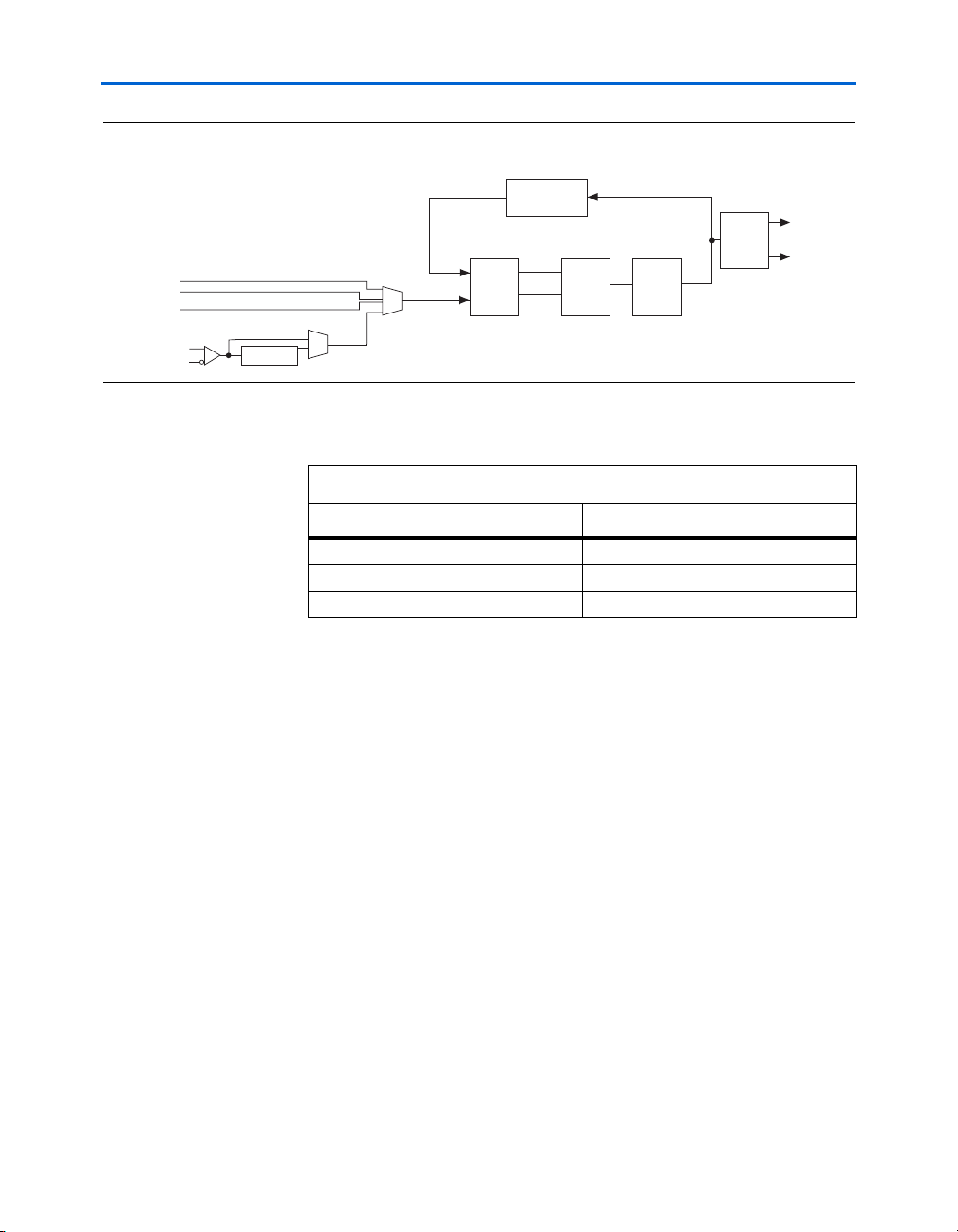
Figure 1–1 shows a block diagram of the gigabit transceiver block (GXB).
You can bypass various modules if desired. Refer to“Modes of
Operation” on page 1–5 for a description of the supported features in
each mode. You can divide the transceiver block into an analog section
and a digital section, as shown in Figure 1–1.
Figure 1–1. Block Diagram of a Stratix GX Gigabit Transceiver Block
Digital SectionAnalog Section
Word
Aligner
Channel
Aligner
8B/10B
Encoder
Rate
Matcher
Reference
Clock
Reference
Clock
Receiver
Transmitter
Deserializer
Clock
Recovery
Unit
Receiver
PLL
Transmitter
PLL
Serializer
8B/10B
Decoder
Serializer
Byte
Byte
Deserializer
Compensation
FIFO Buffer
Phase
Compensation
FIFO Buffer
Phase
Analog Section Overview
This section describes the various components within the analog section
of the transceiver block.
Transmitter Differential I/O Buffers
The gigabit transmitter block differential I/O buffers support the 1.5-V
PCML I/O standard, and contain features that improve system signal
integrity. These features include programmable pre-emphasis, which
helps compensate for high frequency losses, and a variety of
programmable V
Receiver Differential I/O Buffers
The gigabit transceiver block differential I/O buffers support the 1.5-V
PCML I/O standard, and contain a variety of features that improve
system signal integrity. Programmable equalization capabilities are used
to compensate for signal degradation across transmission mediums.
1–2 Altera Corporation
Stratix GX Transceiver User Guide January 2005
settings that support noise margin tuning.
OD
Page 11

Introduction
Transmitter & Receiver PLLs
Each gigabit transceiver block contains one dedicated transmitter PLL
and four dedicated receiver PLLs. These PLLs provide clocking flexibility
and support a range of incoming data streams. For data transmission and
recovery, these PLLs generate the required clock frequencies based upon
the synthesis of an input reference clock. Each transmitter PLL supports
multiplication factors of 2, 4, 5, 8, 10, 16, or 20. Either external reference
clocks or a variety of clock sources within the Stratix GX device drive the
PLLs.
Clock Recovery Unit
The gigabit transceiver block clock recovery unit (CRU) performs analog
Clock Data Recovery (CDR). The CRU uses an external reference clock to
extract a recovered clock that is frequency and phase aligned with the
incoming data, thereby eliminating any clock-to-data skew. This
recovered clock then clocks the data through the rest of the gigabit
transceiver block.
Serializer Deserializer (SERDES)
The transmitter serializer converts the incoming lower speed parallel
signal to a high-speed serial signal on the transmit side. The SERDES
supports a variety of conversion factors, ensuring implementation
flexibility. For example, the SERDES supports 10- and 20-bit serialization
factors, typically required for 8B/10B encoded data, as well as 8- and
16-bit factors.
The receiver deserializer converts the incoming data stream from a
high-speed serial signal to a lower-speed parallel signal that can be
processed in the FPGA logic array on the receive side. The SERDES
supports a variety of conversion factors, ensuring implementation
flexibility. For example, the SERDES supports both 10-bit and 8-bit
serialization and deserialization factors.
Digital Overview
This section describes the various components in the digital section of the
transceiver block.
Altera Corporation 1–3
January 2005 Stratix GX Transceiver User Guide
Page 12

Transceiver Block Architecture
Transmitter & Receiver Phase Compensation FIFO Buffer
The transmitter and receiver data path has a dedicated phase
compensation FIFO buffer that decouples phase variations between the
FPGA and transceiver clock domains. These FIFO buffers ensure a
consistent, reliable interface to the logic array and simplify system design
and timing analysis.
Byte Serializer/Deserializer
The byte serializer converts a 16- or 20-bit data bus into two 8- or 10-bit
data buses, respectively, at double the data rate. The byte serializer
converts an 8- or 10-bit data bus into 16- or 20-bit data buses, allowing
maximum throughput of the transceiver without burdening the FPGA
logic array.
The byte deserializer converts an 8- or 10-bit data bus into 16- or 20-bit
data buses, allowing maximum throughput of the transceiver without
burdening the FPGA logic array.
8B/10B Encoder/Decoder
8B/10B encoding/decoding is the backbone of many transceiver
protocols, and it is often used in proprietary implementations. The
gigabit transceiver block has dedicated circuitry to perform 8B/10B
encoding in the transmitter and decoding in the receiver. This coding
technique ensures sufficient data transitions and a DC balanced stream in
the data signal for successful data recovery at the receiver.
Word Aligner
The word aligner module contains a fully programmable pattern detector
to identify specific patterns within the incoming data stream. The pattern
detector includes recognition support /K28.5/ comma characters for
8B/10B encoded data and A1 or A2 frame alignment patterns for
scrambled signals. Additionally, you can specify a custom alignment
pattern in lieu of the /K28.5/ comma.
The word aligner in the gigabit transceiver block also creates words from
the incoming serial data stream by realigning the data based on identified
byte boundaries. The realignment function uses a barrel shifter and
works with the pattern detector. Additionally, the word aligner has a
manual data realignment mode that lets you control the data realignment
in user mode without consistent alignment characters.
1–4 Altera Corporation
Stratix GX Transceiver User Guide January 2005
Page 13

Introduction
Channel Aligner
An embedded channel aligner aligns byte boundaries across multiple
channels and synchronizes the data entering the logic array from the
gigabit transceiver block’s four channels. The Stratix GX channel aligner
is optimized for a 10-Gigabit Ethernet XAUI 4-channel implementation.
The channel aligner includes the control circuitry and channel alignment
character detection defined by the XAUI protocol. The channel aligner is
only available in XAUI mode.
Rate Matcher
In multi-crystal environments, the clock frequencies of the transmitting
and receiving devices do not match. This mismatch can cause the data to
transmit at a rate slightly faster or slower than the receiving device can
interpret. The Stratix GX rate matcher resolves the frequency differences
between the recovered clock and the FPGA logic array clock by inserting
or deleting removable characters from the data stream, as defined by the
transmission protocol, without compromising transmitted data. If the
functional mode is XAUI, the rate matcher is based on the 10-Gigabit
Ethernet protocol. If the functional mode is GigE, the rate matcher is
based on the Gigabit Ethernet protocol.
Modes of Operation
You can bypass various modules of the gigabit transceiver block based on
the configured mode of operation. Stratix GX transceivers currently
support basic mode, SONET mode, and XAUI mode. This section
provides an overview of each supported mode of operation.
Basic Mode
Basic mode enables a subset of the transceiver blocks so you can perform
customizable configuration. Channel aligner and the rate matcher
features are not available in this mode. Refer to the Basic Mode chapter for
more details on the configurability of this mode. Figure 1–2 shows a block
diagram of a duplex channel configured in basic mode.
Altera Corporation 1–5
January 2005 Stratix GX Transceiver User Guide
Page 14
Modes of Operation
Figure 1–2. Block Diagram of a Duplex Channel Configured in Basic Mode
Digital SectionAnalog Section
Reference
Clock
Reference
Clock
Receiver
Transmitter
Deserializer
Clock
Recovery
Unit
Receiver
PLL
Transmitter
PLL
Serializer
Word
Aligner
Channel
Aligner
8B/10B
Encoder
Rate
Matcher
8B/10B
Decoder
Serializer
Byte
Byte
Deserializer
Compensation
FIFO Buffer
Phase
Compensation
FIFO Buffer
Phase
SONET Mode
SONET mode lets you to select a subset of the transceiver blocks to
perform SONET-like configuration. SONET-like implies that the data
width can either be 8 or 16 bits and that the 8B/10B encoder/decoder,
channel aligner, and the rate matcher features are not available. Refer to
the SONET Mode chapter for more details on the configurability of this
mode. Figure 1–3 shows a block diagram of a duplex channel configured
in SONET mode.
1–6 Altera Corporation
Stratix GX Transceiver User Guide January 2005
Page 15
Figure 1–3. Block Diagram of a Duplex Channel Configured in SONET Mode
Digital SectionAnalog Section
Introduction
Reference
Clock
Reference
Clock
Receiver
Transmitter
Deserializer
Clock
Recovery
Unit
Receiver
PLL
Transmitter
PLL
Serializer
Word
Aligner
Channel
Aligner
8B/10B
Encoder
Rate
Matcher
8B/10B
Decoder
Serializer
Byte
Byte
Deserializer
Compensation
FIFO Buffer
Phase
Compensation
FIFO Buffer
Phase
XAUI Mode
Stratix GX transceivers contain embedded macros dedicated to
supporting the XAUI protocol, specified in clause 47 of the IEEE 802.3ae
specification. These macros includes synchronization, channel deskew,
rate matching, XGXS to XGMII, and XGMII to XGXS code-group
conversion. Refer to the XAUI Mode chapter for more details on the
configurability of this mode. Figure 1–4 shows a block diagram of a
duplex channel configured in XAUI mode.
Altera Corporation 1–7
January 2005 Stratix GX Transceiver User Guide
Page 16
Modes of Operation
Figure 1–4. Block Diagram of a Duplex Channel Configured in XAUI Mode
Digital SectionAnalog Section
Reference
Clock
Reference
Clock
Receiver
Transmitter
Deserializer
Clock
Recovery
Unit
Receiver
PLL
Transmitter
PLL
Serializer
Word
Aligner
Channel
Aligner
8B/10B
Encoder
Rate
Matcher
8B/10B
Decoder
Serializer
Byte
Byte
Deserializer
Compensation
FIFO Buffer
Phase
Compensation
FIFO Buffer
Phase
GigE Mode
Stratix GX devices in GigE mode can use the 8B/10B encoder/decoder,
rate matcher, synchronizer, and byte serializer/deserializer built-in hard
macros. Refer to the GigE Mode chapter for more information about this
mode. The rate matcher and word aligner each have a dedicated state
machine governing their functions. These state machines are active only
in GigE mode. Figure 1–5 shows a block diagram of a duplex channel
configured in GigE mode.
1–8 Altera Corporation
Stratix GX Transceiver User Guide January 2005
Page 17
Figure 1–5. Block Diagram of a Duplex Channel Configured in GigE Mode
Digital SectionAnalog Section
Introduction
Reference
Clock
Reference
Clock
Receiver
Transmitter
Deserializer
Clock
Recovery
Unit
Receiver
PLL
Transmitter
PLL
Serializer
Word
Aligner
Channel
Aligner
8B/10B
Encoder
Rate
Matcher
8B/10B
Decoder
Byte
Serializer
Byte
Deserializer
Phase
Compensation
FIFO Buffer
Phase
Compensation
FIFO Buffer
Loopback
There are three different loopback modes to use in the gigabit transceiver
block to allow for a complete method of in-system verification. The
loopback modes are versatile and robust enough to accommodate all
protocols and let you to choose whether to retime the data.
Built-In Self Test
The gigabit transceiver block contains several features that simplify
design verification. An embedded PRBS pattern generator provides a
bitstream pattern that you can use to test the device and board
connections. The PRBS pattern generator works with a PRBS receiver to
implement a full self-test path. Additionally, serial and parallel loopback
paths let you test the FPGA logic without monitoring external signals.
The reverse loopback path enables external system testing with minimal
device interaction.
Altera Corporation 1–9
January 2005 Stratix GX Transceiver User Guide
Page 18

Modes of Operation
1–10 Altera Corporation
Stratix GX Transceiver User Guide January 2005
Page 19

2. Stratix GX Analog Description
Introduction
This chapter describes how to serialize the parallel data for transmission
and convert received data into parallel data. Data transmission and
reception is performed by pseudo current mode logic (PCML) buffers.
These transceiver buffers support programmable pre-emphasis,
equalization, and programmable V
The programmable pre-emphasis setting is available on transmit buffers
to maximize the eye opening on the far-end receiver by boosting the
high-frequency component of the data signal. Similarly, programmable
equalization is available for receive buffers to reduce the high-frequency
losses and inter-symbol interference. These features are useful in lossy
transmission lines. Transceivers also support flexible reference clock
generation capabilities, including a dedicated transmitter phase-locked
loop (PLL) and four receiver PLLs per transceiver block.
The clock recovery unit (CRU) is the main part of each receive analog
section; it recovers the clock from the serial data stream (see Figure 2–1).
You can set the CRU to automatically or manually alter the receiver PLL
phase and frequency to match the bit transition on the incoming data
stream. This is to eliminate any clock-to-data skew or to keep the receiver
PLL locked to the reference clock (lock-to-data or lock-to-reference
mode).
During the clock recovery phase, the receiver PLL initially locks to the
reference clock and then attempts to lock on to the incoming data by first
recovering the clock from the incoming serial data.
settings in I/O buffers.
OD
Altera Corporation 2–1
January 2005
Page 20
Transmitter Analog
Figure 2–1. Block Diagram Analog Components
Digital SectionAnalog Section
Deserializer
Clock
Recovery
Unit
Reference
Clock
Reference
Clock
Receiver
Transmitter
Receiver
PLL
Transmitter
PLL
Serializer
Transmitter
Word
Aligner
Channel
Aligner
This section describes the transmitter buffer, the transmitter PLL, and the
serializer. Figure 2–2 shows the transmitter analog components.
Analog
Figure 2–2. Transmitter Analog Components
Digital SectionAnalog Section
Reference
Clock
Transmitter
PLL
8B/10B
Encoder
Rate
Matcher
8B/10B
Decoder
Serializer
Byte
Byte
Deserializer
Compensation
FIFO Buffer
Phase
Compensation
FIFO Buffer
Phase
Transmitter
Serializer
8B/10B
Encoder
Byte
Serializer
Phase
Compensation
FIFO Buffer
Transmitter Buffer
The Stratix®GX transceiver buffers support the 1.5-V PCML standard at
speeds up to 3.1875 gigabits per second (Gbps) and are capable of driving
40 inches of FR4 trace across two connectors. In addition, the buffer
contains programmable output voltage, programmable pre-emphasis
circuitry, and internal termination circuitry.
2–2 Altera Corporation
Stratix GX Transceiver User Guide January 2005
Page 21
Programmable Voltage Output Differential (VOD)
Stratix GX transceivers let you customize the differential output voltage
) to handle different length, backplane, and receiver requirements
(V
OD
(see Figure 2–3). You can select the VOD (differential) from a range of 400
to 1,600 mV, as shown in Table 2–1.
Figure 2–3. VOD (Differential) Signal Level
Single-Ended Waveform
V
CM
Differential Waveform (VOD (Differential) = 2 x VOD (single-ended))
V
OD
Stratix GX Analog Description
Positive Channel (p) = V
V
OD
Negative Channel (n) = V
Ground
p − n = 0 V
V
OD
OH
OL
Table 2–1 shows the differential output voltage (VOD) setting per current
level for each of the on-chip transmitter programmable termination
values.
Table 2–1. Programmable VOD (Differential)
100 Ω (mV) 120 Ω (mV) 150 Ω (mV)
400 480 600
800 960 1,200
1,000 1,200 1,500
1,200 1,440
1,400
1,600
Altera Corporation 2–3
January 2005 Stratix GX Transceiver User Guide
Page 22

Transmitter Analog
You can set the differential VOD values statically during configuration or
dynamically adjust them in user mode. You select the static V
through a list in the altgxb MegaWizard
the appropriate V
setting in the configuration file. The disadvantage of
OD
®
Plug-In Manager, which sets
OD
value
the static mode setting is that the VOD is set on a per transceiver block
basis and cannot be changed unless you regenerate another
programming file.
Alternatively, if you enable dynamic adjustment in the altgxb
MegaWizard Plug-In, you can dynamically configure the V
setting by
OD
the device during user mode. This configuration is done by asserting
encoded values on the tx_vodctrl bus, which is instantiated in the
altgxb module when you select the dynamic adjustment option. This
option lets you make quick performance evaluations of the various
settings without having to recompile and regenerate multiple
configuration files. Another advantage of this option is that it allows the
of each channel to be configured independently. Refer to the section
V
OD
“MegaWizard Analog Features” on page 2–20 for further details.
Programmable Pre-Emphasis
The programmable pre-emphasis module in each transmit buffer boosts
the high frequencies in the transmit data signal, which may be attenuated
in the transmission media. This maximizes the data eye opening at the
far-end receiver. Pre-emphasis is particularly useful in lossy transmission
mediums.
The transfer function of a transmission line can be represented in the
frequency domain as a low-pass filter. Any frequency components below
the –3 dB frequency pass through with minimal losses. Frequency
components that are greater than the –3-dB frequency are attenuated.
This variation in frequency response yields data-dependant jitter and
other ISI effects. By applying pre-emphasis, the high frequency
components are boosted, or in other words, pre-emphasized. This
pre-emphasis equalizes the frequency response as seen at the receiver so
that the delta between the low-frequency and high-frequency
components is reduced, which in return minimizes the ISI effects from the
transmission medium.
In Stratix GX transceivers, the programmable pre-emphasis settings can
have one of six values (0 to 5). You should experiment with the
pre-emphasis values to determine the optimal setting based on your
system variables.
2–4 Altera Corporation
Stratix GX Transceiver User Guide January 2005
Page 23

Stratix GX Analog Description
As with the VOD settings, you can set the pre-emphasis settings statically
during configuration or adjust them dynamically in user mode. You can
set the static pre-emphasis value through a drop-down menu in the
altgxb MegaWizard Plug-In, which sets the appropriate pre-emphasis
setting in the configuration file. The disadvantage of the static mode
setting is that the pre-emphasis is set on a per-transceiver-block basis and
cannot be changed without regenerating another programming file.
On the other hand, if you select dynamic adjustment in the altgxb
MegaWizard Plug-In, the pre-emphasis setting can be configured
dynamically by the device during user mode. This configuration is done
by asserting encoded values on the tx_preemphasisctrl bus, which
is instantiated in the altgxb module when you select the dynamic
adjustment option. This option lets you make quick performance
evaluations of the various settings without having to recompile and
regenerate multiple configuration files. Another advantage of this option
is that it allows the pre-emphasis of each channel to be configured
independently. For further details, refer to “MegaWizard Analog
Features” on page 2–20.
Avoid pre-emphasis and V
settings that yield a value greater than
OD
1,600 mV. Settings beyond this value do not damage the buffer, but they
prevent accurate device operation. Verify that the combination of V
OD
and pre-emphasis settings do not exceed the 1,600-mV limit.
Programmable Transmitter Termination
The Stratix GX transmitter buffer includes a 100-, 120-, or 150-Ω
programmable on-chip differential termination resistor. The Stratix GX
transmitter buffers are current-mode drivers, so the resultant V
OD
is a
function of the transmitter termination value. For more information on
resultant V
values, see “Programmable Voltage Output Differential
OD
(VOD)” on page 2–3.
Transmitter PLL
Each transceiver block contains a transmitter PLL and a slow-speed
reference clock. The transmitter PLL receives the reference clock and
generates the high-speed serial clock used by the serializer. The slowspeed reference clock is used for the transceiver logic. Figure 2–4 shows
the transmitter PLL’s block diagram. The pll_locked signal indicates
when the transmitter PLL is locked to the reference clock. A high signal
indicates that the PLL is locked to the reference clock; a low signal
indicates that the PLL is not locked to the reference clock.
Altera Corporation 2–5
January 2005 Stratix GX Transceiver User Guide
Page 24
Transmitter Analog
Figure 2–4. Transmitter PLL Block Diagram
Inter Quad Routing (IQ1)
Inter Quad Routing (IQ0)
Global Clocks, I/O Bus, General Routing
/4, 8, 10, 16, 20
/m
Up
PFD CP+LF
DownINCLK
VCO
Clock
Driver
High Speed
TX_PLL_CLK
Low Speed
TX_PLL_CLK
Dedicated Local
REFCLKB
/2
Table 2–2 lists some of the transmitter PLL specifications.
Table 2–2. Transmitter PLL Specifications
Parameter Specifications
Input reference frequency range 25 MHz to 650 MHz
Data rate support 500 Mbps to 3.1875 Gbps
Multiplication factor (W) 2, 4, 5, 8, 10, 16, or 20 (1)
Note to Ta b l e 2 – 2:
(1) Multiplication factors 2 and 5 can only be achieved with the use of the pre-divider
on the REFCLKB.
Clock Synthesis
The maximum input frequency of the phase frequency detector (PFD) is
325 MHz. To achieve reference clock frequency above this limitation, the
/2 pre-divider on the dedicated local REFCLKB path can be enabled
automatically by the Quartus
reference clock frequency by a factor of 2 and then the /m factor
compensates the frequency difference. An example would be a data rate
of 2,488 Mbps with a 622-MHz reference clock. In this scenario, the
reference clock must be assigned to the REFCLKB port where the 622MHz reference clock is divided by 2, yielding a 311-MHz clock at the PFD.
This 311-MHz reference clock is then multiplied by a factor of 8 to achieve
the 2,488-MHz clock at the VCO.
®
II software. The /2 pre-divider divides the
2–6 Altera Corporation
Stratix GX Transceiver User Guide January 2005
Page 25
Stratix GX Analog Description
If the reference clock exceeds 325 MHz, the clock must be fed by the
dedicated local reference clock pin, REFCLKB. By default, the Quartus II
software assigns pins to be LVTTL, so you must assign the 1.5-V PCML
I/O standard to the I/O pins to select the REFCLKB port as the reference
source. The Quartus II software prompts a fitter error if the reference
clock exceeds 325 MHz and the reference clock source is not on the
REFCLKB port.
You can also use the pre-divider on the REFCLKB path to support
additional multiplication factors. The block diagram in Figure 2–4 shows
that /m can only support multiplication factors of 4, 8, 10, 16, and 20, but
Table 2–3 shows that the additional multiplication factors of 2 and 5 are
also achievable. You can achieve these multiplication factors by using the
pre-divider. A multiplication factor of 2 is achieved by pre-dividing the
reference clock by 2 and then multiplying the resultant frequency by 4,
which yields a multiplication factor of 2. A multiplication factor of 5 is
achieved in the same manner by pre-dividing the reference clock by 2 and
then multiplying the resultant frequency by 10, which yields a
multiplication factor of 5.
Table 2–3 lists the possible multiplication values as a function of the
source to the transmitter PLL. Table 2–3 assumes that the reference clock
is directly fed from the source listed and does not factor any pre-clock
synthesis (that is, the Stratix GX PLL driving a global clock that is used for
the transmitter PLL reference clock source).
Table 2–3. Multiplication Values as a Function of the Reference Clock
Source to the Transmitter PLL
Transmitter PLL Reference Clock
Source
Global clock, I/O bus, general routing 4, 8, 10, 16, 20
Inter-transceiver routing 2, 4, 5, 8, 10, 16, 20
Dedicated local REFCLKB 2, 4, 5, 8, 10, 16, 20
Multiplication Factors
You must specify the data rate of the channel and input clock period of
the reference clock. The data rate divided by the input clock period must
equal one of the multiplication factors listed in Table 2–3.
Transmitter PLL Bandwidth Setting
The Stratix GX transmitter PLL in the transceiver block offers a
programmable bandwidth setting. The PLL bandwidth is the measure of
its ability to track the input clock and jitter. The bandwidth is determined
by the –3-dB frequency of the closed-loop gain of the PLL.
Altera Corporation 2–7
January 2005 Stratix GX Transceiver User Guide
Page 26
Transmitter Analog
A high-bandwidth setting provides a faster lock time and tracks more
jitter on the input clock source which passes it through the PLL. This
helps reject noise from the VCO and power supplies. A low-bandwidth
setting, on the other hand, filters out more high frequency input clock
jitter, but increases lock time.
You can set the bandwidth for Stratix GX devices to either low or high.
The –3-dB frequencies for these settings can vary due to the non-linear
nature and frequency dependencies of the circuit. As a result, you can
vary the bandwidth to customize the performance on specific systems.
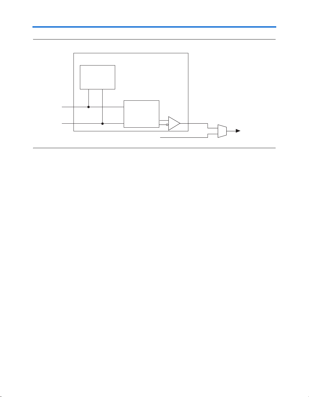
Serializer (Parallel-to-Serial Converter)
The serializer converts parallel data to serial data at the transmitter
output buffer. The serializer can support 8- or 10-bit words when used
with the transmitter multiplexer. The 8-bit serializer drives the serial data
to the output buffer, as shown in Figure 2–5. The serializer can drive the
serial bit-stream at a data rate range of 500 Mbps to 3.1875 Gbps. The
serializer outputs the least significant bit (LSB) of the word first.
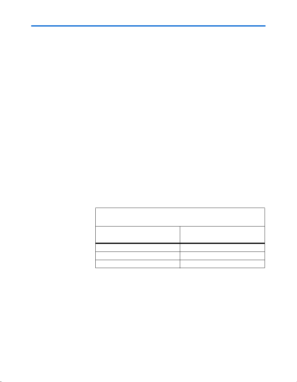
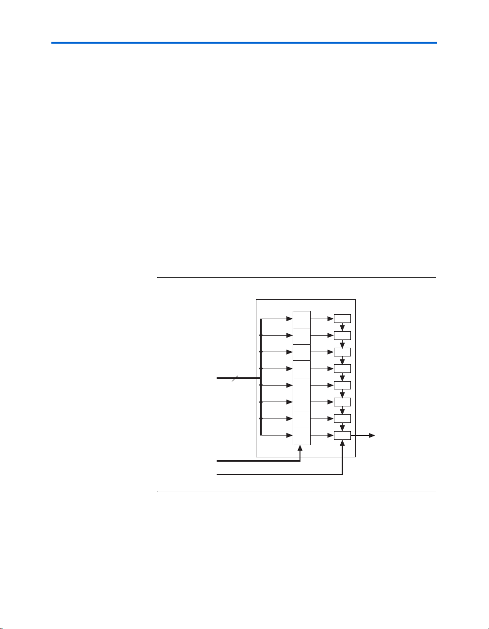
Figure 2–5. Example of 8-Bit Serialization
Serializer
D7
D8
D6
D4
D3
D2
D1
D0
Serial Data Out
(I/O Output Buffer)
Parallel Data
D7
D8
D6
8
D4
D3
D2
D1
D0
Low-Speed
Parallel Clock
High-Speed
Serial Clock
Figure 2–6 shows the serial bit order of the serializer output. In this
example, a constant 8’h6a (01010110) value is serialized.
1 The serial data is transmitted from LSB to most significant bit
(MSB).
2–8 Altera Corporation
Stratix GX Transceiver User Guide January 2005
Page 27
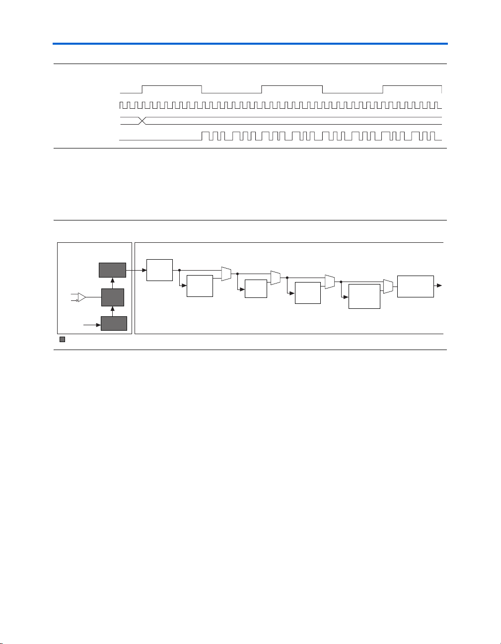
Figure 2–6. Serializer Bit Order
Parallel Clock
Serial Clock
Parallel Data (in Hex)
Serial Data Out
(x) 56
Stratix GX Analog Description
011 01 010
Receiver Analog
This section describes the receiver input buffer, the receiver PLL, the clock
recovery unit, and the deserializer. Figure 2–7 shows the receiver analog
components.
Figure 2–7. Highlighted Block Diagram of the Receiver Analog Components
Digital SectionAnalog Section
Word
Aligner
Channel
Aligner
Rate
Matcher
8B/10B
Decoder
Reference
Clock
Receiver
Deserializer
Clock
Recovery
Unit
Receiver
PLL
Receiver Input Buffer
The receiver input buffer contains internal termination and internal
equalization. Figure 2–8 shows the structure of the input buffer. The input
buffer has programmable equalization that you can apply to increase the
signal integrity of the transmission line. The internal termination in the
receiver buffer can support AC and DC coupling with programmable
differential termination settings of 100, 120, or 150 Ω..
Byte
Deserializer
Phase
Compensation
FIFO Buffer
Altera Corporation 2–9
January 2005 Stratix GX Transceiver User Guide
Page 28
Receiver Analog
Figure 2–8. Receiver Input Buffer
Input Buffer
Programmable
Termination
Input Pins
Programmable
Equalizer
Internal Loopback
from Transmitter
To PLD
Programmable Receiver Termination
The Stratix GX receiver buffer includes programmable on-chip
differential termination of 100, 120, or 150 Ω..
This assignment must be made per pin through the Assignment Editor in
the Quartus II software. Select Assignment Organizer > Options for
Individual Nodes Only > Stratix GX Termination Value (Assignments
menu).
1 The proper termination settings should be selected and verified
accordingly before compilation.
The transmitter PLL input signal (inclk) drives the termination
resistance calibration circuit. The Quartus II software allows
receiver-only configurations in Stratix GX devices. However, if you use
the Quartus II software to remove the transmitter PLL in a receiver-only
configuration, you will see an incorrect value or unpredictable behavior
with the receiver input pin termination. If the rx_cruclk signal is
globally routed, the Quartus II software handles this automatically. If the
rx_cruclk signal is not globally routed or routed using the interquadrant line (IQ2), the Quartus II software returns a no-fit. In this
situation, you must add a transmitter PLL to your design.
If the pll_areset (analog reset) signal goes high, the RX_Vcm value is
less than the 1.1 V. This value varies unpredictably because the circuit is
tristated. RX_Vcm is referenced from the Stratix GX receiver analog power
supply.
2–10 Altera Corporation
Stratix GX Transceiver User Guide January 2005
Page 29
Stratix GX Analog Description
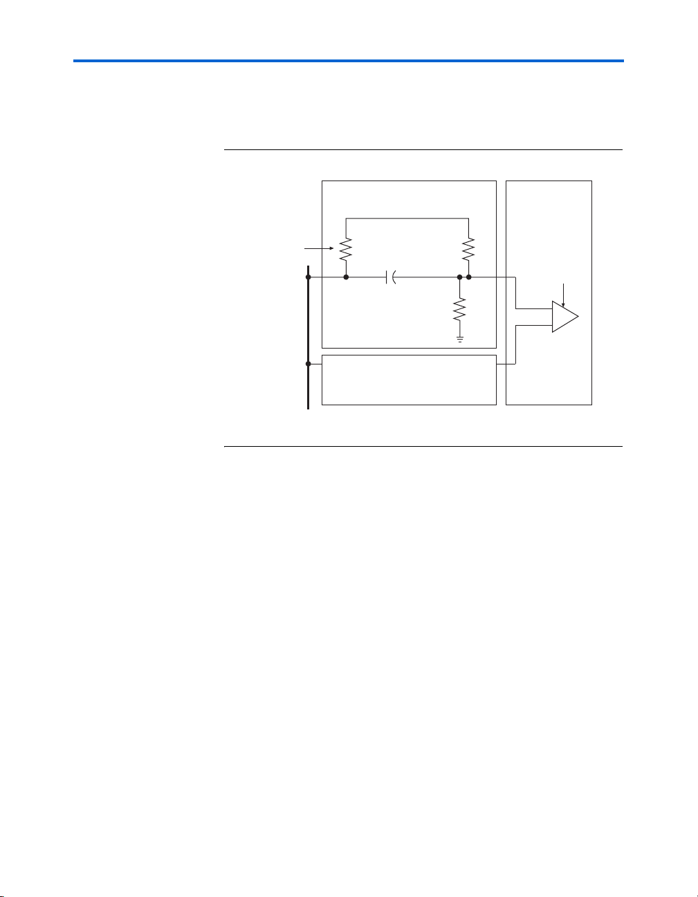
If external termination is used, the receiver must be externally terminated
and biased to 1.1 V. Figure 2–9 shows an example of an external
termination and biasing circuit.
Figure 2–9. External Termination & Biasing Circuit
50/60/75Termination
Resistance
Transmission
Receiver External Termination
and Biasing
Ω
R1/R2 = 1K
V
× {R2/(R1 + R 2)} = 1.1 V
DD
Receiver External Termination
Line
V
DD
C1
and Biasing
R1
R2
Stratix GX Device
Receiver
RXIP
RXIN
Enable Stratix GX-to-Stratix GX Receiver DC Coupling
You can configure the Stratix GX receiver buffers so that DC-coupled
Stratix GX-to-Stratix GX communication is possible. The Stratix GX
transmitter’s common-mode is typically around 750 mV, while the
receiver common mode by default is approximately 1.1 V. However, by
enabling DC coupling, the receiver common mode is biased to allow
interoperability with the Stratix GX transmitter.
Equalizer Mode
Stratix GX transceivers offer an equalization circuit in each receiver
channel to increase noise margins and help reduce the effects of high
frequency losses. The programmable equalizer compensates for
inter-symbol interference (ISI) and high frequency losses that distort the
signal and reduce the noise margin of the transmission medium by
equalizing the frequency response.
The transfer function of a transmission line can be represented in the
frequency domain as a low-pass filter. Any frequency components below
the –3-dB frequency pass through with minimal losses. Frequency
components that are greater than the –3-dB frequency are attenuated.
Altera Corporation 2–11
January 2005 Stratix GX Transceiver User Guide
Page 30

Receiver Analog
This variation in frequency response yields data-dependant jitter and
other ISI effects. By applying equalization, the low frequency components
are attenuated. This equalizes the frequency response so that the delta
between the low frequency and high frequency components are reduced,
which minimizes the ISI effects from the transmission medium.
In Stratix GX transceivers, the programmable equalizer settings can have
one of five values (0 through four). You should experiment with the
equalization values to determine the optimal setting based on your
system variables.
As with the V
settings, you can set the equalization settings statically
OD
during configuration or adjust them dynamically in user mode. You can
select the static equalization value through a drop-down menu in the
altgxb MegaWizard Plug-In. This action sets the appropriate
equalization setting in the configuration file. The disadvantage of this
mode is that the equalization is set on a per-transceiver block basis and
cannot be changed without regenerating another programming file.
On the other hand, if you select the dynamic adjustment in the altgxb
MegaWizard Plug-In, the equalization setting can be configured
dynamically by the device during user mode. This configuration is
accomplished by asserting encoded values on the rx_equalizerctrl
signal, which is instantiated in the altgxb module when this option is
selected. This feature lets you make quick performance evaluations of the
various settings without having to recompile and regenerate multiple
configuration files. Another advantage is that this option allows the
equalization of each channel to be configured independently. Refer to
“MegaWizard Analog Features” on page 2–20 for more details.
Receiver PLL
Each transceiver block contains four receiver PLLs and a slow-speed
reference clock. The receiver PLLs receive the reference clock and
generate the high-speed serial clock used by the CR. The slow-speed
reference clock is used for the transceiver logic. Figure 2–10 shows the
block diagram for the lock-to-reference portion of the receiver PLL.
This section focuses on the receiver PLL in Lock-to-Reference mode. The
lock-to-data circuit has been omitted. Refer to the “Lock-to-Reference
Mode & Lock-to-Data Mode” on page 2–16 for more information on the
operation between the two modes.
2–12 Altera Corporation
Stratix GX Transceiver User Guide January 2005
Page 31

The receiver PLL contains an optional loss-of-lock indicator signal
(rx_locked) that indicates when the receiver PLL is not locked to the
reference clock. The rx_locked signal is active low. A low signal
indicates that the PLL is locked to a reference clock; a high signal indicates
that the PLL is not locked to the reference clock.
Figure 2–10. Receiver PLL Block Diagram
Stratix GX Analog Description
(1)
÷m
Low speed TX_PLL_CLK
Inter Transceiver Block Routing
Global Clks, I/O Bus, Gen Routing
Dedicated Local
REFCLKB
÷2
Note to Figure 2–10:
(1) m = 8, 10, 16, or 20.
PFD
Up
Down
Up
Down
CP+LF
rx_rlv[ ]
High Speed RCVD_CLK
Low Speed RCVD_CLK
VCO
rx_locktorefclk
rx_locktodata
RX_IN
RX_CRUCLK
Clock Recovery Unit (CRU)
Table 2–4 lists some of the clock recovery unit specifications.
Table 2–4. Clock Recovery Unit Specifications
Parameter Specification
Input reference frequency range 25 MHz to 650 MHz
Data rate support 500 Mbps to 3.1875 Gbps
Multiplication factor (W) 2, 4, 5, 8, 10, 16, or 20 (1)
Note to Ta b l e 2 – 4:
(1) Multiplication factors 2, 4, and 5 can only be achieved with the use of the pre-
divider on the REFCLKB port or if the CRU is trained with the low speed clock
from the transmitter PLL.
Clock Synthesis
The maximum input frequency of the PFD of the receiver PLL is
325 MHz. To achieve reference clock frequency above this limit, the
Quartus II software enables the divide by 2 pre-divider on the dedicated
local REFCLKB path. This divides the reference clock frequency by a factor
of 2 and then the /m factor compensates the frequency difference. For
example, given a data rate of 2,488 Mbps with a reference clock of
622 MHz, the reference clock must be assigned to the REFCLKB port,
Altera Corporation 2–13
January 2005 Stratix GX Transceiver User Guide
Page 32

Receiver Analog
where the reference clock signal is divided by 2, yielding a 311 MHz clock
at the PFD. This 311-MHz reference clock is then multiplied by a factor of
8 to achieve the 2,488-MHz clock at the VCO.
If the reference clock (RX_CRUCLK) exceeds 325 MHz, the clock must be
fed by the dedicated local reference clock pin, REFCLKB. By default, the
Quartus II software assigns pins to be LVTTL, so a 1.5-V PCML I/O
standard assignment is required to select the REFCLKB port as the
reference source. The Quartus II software prompts a fitter error if the
reference clock exceeds 325 MHz and the reference clock source is not on
the REFCLKB port.
The pre-divider on the REFCLKB path is also used to support additional
multiplication factors. The block diagram in Figure 2–10 on page 2–13
shows that /m supports only multiplication factors of 8, 10, 16, and 20,
but Table 2–4 states that the additional multiplication factors of 2, 4, and
5 can also be achieved.
Without using the transmitter PLL, the pre-divider achieves the
multiplication factors of 4 and 5. A multiplication factor of 4 is achieved
by pre-dividing the reference clock by 2 and then multiplying the
resulting frequency by 8, which yields a multiplication factor of 4. A
multiplication factor of 5 is achieved in the same manner by pre-dividing
the reference clock by 2 and then multiplying the resulting frequency by
10, which yields a multiplication factor of 5.
The MegaWizard Plug-In altgxb option enables the transmitter PLL in
receiver mode. There is also an option to train the receiver CRU with the
output of the low-speed transmitter PLL clock. If you select this option,
all the multiplication factors that are supported in the transmitter PLL are
also supported in the receiver CRU PLL, including the multiplication
factor of 2. This option selects the low-speed transmitter PLL clock as the
reference source. The low speed transmitter PLL clock is either divided by
a SERDES factor of 8 or 10. The receiver PLL then multiplies this reference
clock by a factor of 8 or 10 to achieve the same multiplication factor as the
transmitter PLL.
For example, a multiplication factor of 2 is achieved on the transmitter
PLL by pre-dividing the reference clock by 2 and then multiplying the
resultant frequency by 4, which yields a multiplication factor of 2.
However, on the low-speed clock output, this frequency is divided by a
factor of 8 or 10, depending on the deserialization factor. The low-speed
clock feeds the reference of the receiver PLL where the clock is multiplied
back up by a factor of 8 or 10, which results in total multiplication factor
of 2.
2–14 Altera Corporation
Stratix GX Transceiver User Guide January 2005
Page 33

Stratix GX Analog Description
Table 2–5 lists the possible multiplication values as a function of the
reference clock source to the receiver PLL. Table 2–5 assumes that the
reference clock (RX_CRUCLK) is directly fed from the source listed and
does not factor any pre-clock synthesis (that is, a Stratix GX PLL driving
a global clock used for the receiver PLL reference clock source).
Table 2–5. Multiplication Values as a Function of the Reference Clock
Source to the Receiver PLL
Receiver PLL Reference Clock Source Multiplication Factors
Global clock, IO bus, general routing 8, 10, 16, 20
Inter-transceiver routing 4, 5, 8, 10, 16, 20
Dedicated local REFCLKB 4, 5, 8, 10, 16, 20
Low-speed transmitter PLL clock
(train CRU with transmitter PLL option)
2, 4, 5, 8, 10, 16, 20
You specify the data rate of the channel and receiver CRU clock period of
the receiver reference clock. The data rate divided by the input clock
period must equal one of the multiplication factors listed in Table 2–5.
PPM Frequency Threshold Detector
The PPM frequency threshold detector senses whether the incoming
reference clock to the CRU and the PLL VCO of the CRU are within a
prescribed PPM tolerance range. Valid parameters are 125, 250, 500, or
1,000 PPM. The default parameter, if no assignments are made, is
1,000 PPM. The output of the PPM frequency threshold detector is one of
the variables that asserts the rx_freqlocked signal. Refer to “Clock
Recovery Unit” on page 2–16 for more detail regarding the
rx_freqlocked signal.
Receiver Bandwidth Type
The Stratix GX receiver PLL in the CRU offers a programmable
bandwidth setting. The bandwidth of a data recovery PLL is the measure
of its ability to track the input data and jitter. The bandwidth is
determined by the –3-dB frequency of the closed-loop gain of the PLL.
A higher bandwidth setting provides a faster lock time and tracks greater
jitter on the input data source, rx_in[], which passes it through the PLL.
This helps reject noise from the VCO and power supplies. A
low-bandwidth setting, on the other hand, filters out more
high-frequency data input jitter, but increases lock time.
Altera Corporation 2–15
January 2005 Stratix GX Transceiver User Guide
Page 34

Receiver Analog
Valid receiver bandwidth settings are low, medium, and high. The –3-dB
frequencies for these settings vary due to the non-linear nature and data
dependencies of the circuit. You vary the bandwidth to customize the
performance on specific systems.
Clock Recovery Unit
The CRU in each Stratix GX receiver channel recovers the clock from the
serial data stream on RX_IN. You can set the CRU to automatically or
manually alter the receiver PLL phase and frequency to match the bit
transition on the incoming data stream. This is to eliminate any
clock-to-data skew or to keep the receiver PLL locked to the reference
clock (lock-to-data or lock-to-reference mode). The CRU generates two
clocks, a high-speed RCVD_CLK to feed the deserializer and a low-speed
RCVD_CLK to feed transceiver logic. You can set the CRU to optionally
detect run-length violations in the incoming data stream and generate an
error whenever the preset run length is exceeded (run-length violation
detection circuit).
Lock-to-Reference Mode & Lock-to-Data Mode
The Stratix GX device offers both automatic and manual locking options,
as described in the following sections.
Automatic Lock Mode
By default, the CRU initially locks to the CRU reference clock RX_CRUCLK
(lock-to-reference mode) until conditions warrant the switchover to the
incoming data (lock-to-data mode). The device switches to the
lock-to-data mode when the rx_freqlocked signal goes high. After
switching to lock-to-data mode, the CRU requires more time to lock to the
incoming serial data.
f For information about the CRU to serial data lock time, which includes
frequency lock (during lock-to-reference mode) and phase lock (during
lock-to-data mode), refer to the Stratix GX FPGA Family data sheet. Also
refer to the Reset Control & Power Down chapter for the recommendations
on resets.
To automatically transition from the lock-to-reference mode to the
lock-to-data mode, the following conditions must be met:
■ The CRU PLL is within the prescribed PPM frequency threshold
setting (125, 250, 500, or 1,000 PPM) of the CRU reference clock.
■ Reference clock and CRU PLL output are phase matched (phases are
within 0.08 UI).
2–16 Altera Corporation
Stratix GX Transceiver User Guide January 2005
Page 35

Stratix GX Analog Description
During the lock-to-reference mode, the frequency detector determines
whether the reference clock to the receiver PLL and the VCO output are
within the prescribed PPM setting.
The phase lock happens when the phase-frequency detector up/down
transitions are relatively few and, the pulse widths are sufficiently
narrow. These conditions show that the PLL is close to absolute phase
lock to the reference clock. This ensures that when actual data signals are
sampled, the receiver PLL locks to the fundamental REFCLK frequency
and does not drift off to any sub-harmonic.
In lock-to-data mode, the PLL uses a phase detector to keep the recovered
clock aligned properly with the data. If the PLL does not stay locked to
data because of problems such as frequency drift or severe amplitude
attenuation, the receiver PLL locks back to the reference clock of the CRU
to train the VCO. When the device is in lock-to-data mode, the CRU tries
to align itself with incoming data and there is no phase relationship with
the reference clock.
In lock-to-data mode, the rx_freqlocked signal is asserted, and the
rx_locked signal looses its significance. The rx_locked signal
signifies that the CRU has locked to the reference clock. When the CRU is
in lock-to-data mode, the rx_locked signal behavior is not predictable.
In automatic lock mode, CRU is forced out of lock-to-data mode if the
CRU PLL is not within the recommended PPM frequency threshold
setting (125 PPM, 250 PPM, 500 PPM, 1000 PPM) of the CRU reference
clock.
When the CRU goes out of lock-to-data mode, the rx_freqlocked
signal goes low. The rx_freqlocked signal also goes low when either
the rx_analogreset or pll_areset signal goes high. The
rx_analogreset signal powers down the receiver and the
pll_areset signal powers down the entire transceiver block (four
channels).
Manual Lock Options
Two optional input pins, rx_locktorefclk[] and
rx_locktodata[], are available that let you control whether the CRU
PLL automatically or manually switches between lock-to-reference clock
and lock-to-data modes. This lets you bypass the default automatic
switchover circuitry if either the rx_locktorefclk[] or
rx_locktodata[] signal is instantiated.
When the rx_locktorefclk[] signal is asserted, it forces the CRU PLL
to lock to the reference clock (RX_CRUCLK). Asserting the
rx_locktodata[] signal forces the CRU PLL to lock to data, whether
Altera Corporation 2–17
January 2005 Stratix GX Transceiver User Guide
Page 36

Receiver Analog
or not the CRU is ready. When both signals are asserted, the
rx_locktodata[] signal takes precedence over the
rx_locktorefclk[] signal.
You might want to have control over both rx_locktorefclk[] and
rx_locktodata[] signals to potentially reduce the CRU lock times.
The PPM threshold frequency detector and phase relationship detector
require additional latencies to ensure that the CRU is ready to lock to
data. These extra latencies are potentially reduced by manually
controlling the CRU train signals. You assert the rx_locktorefclk[]
signal to initially train the CRU and, after some delta time, assert the
rx_locktodata[] signal.
You configure the controller that controls the signals based on your
system. You do this by experimenting because many variables must be
considered, such as temperature, transition densities, and data rates.
However, by doing so, you are not subjected to the CRU lock times
required to verify if the two conditions to switch from lock-to-reference
mode to lock-to-data mode in the defaulted automatic mode are met.
When the rx_locktorefclk goes high, the rx_freqlocked signal is
ignored and does not toggle. The rx_freqlocked signal always goes
high if lock-to-data mode is asserted. If you want to transition from
lock-to-data mode to automatic mode, the transition should be followed
by rx_analogreset to send the rx_freqlocked signal low. The CRU
does not often transition from manual mode to automatic mode during
system operation.
1 The rx_analogreset signal functions like a power down
signal as opposed to a digital reset. For more information on
various reset signals, refer to the chapter Reset Control & Power
Down.
Run Length Violation Detection Circuit
The programmable run length violation (RLV) circuit is in the CRU and
detects consecutive ones or zeros in the data. If the data stream exceeds
the preset maximum number of consecutive ones or zeros, the violation is
signified by the assertion of the rx_rlv signal.
The rx_rlv signal is not synchronized to the parallel data, and as a result
appears in the logic array earlier than the run-length violation data. To
ensure that the FPGA latches this signal in systems where there are
frequency variations between the recovered clock and the PLD logic array
clock, the rx_rlv signal is asserted for more than two clock cycles in 8or 10-bit data modes and three clock cycles in 16- or 20-bit data modes.
2–18 Altera Corporation
Stratix GX Transceiver User Guide January 2005
Page 37

Stratix GX Analog Description
If the data width is 8 or 16, set the legal run length threshold values within
the range of 4 to 128 UI in multiples of four. If the data width is 10 or 20,
or if using 8b10b, set the legal run length threshold values within the
range of 5 to 160 UI in multiples of five.
1 See the Stratix GX FPGA Family data sheet to verify the
guaranteed maximum run length.
Deserializer (Serial-to-Parallel Converter)
The deserializer converts incoming high-speed serial data streams to
either 8- or 10-bit-wide parallel data synchronized to the recovered clock
of the CRU. The deserializer drives the parallel data to the pattern
detector and word aligner, as shown in Figure 2–11. The data rate of the
deserializer output bus is the input data rate divided by the width of the
output data bus. For example, for a 10-bit bus and a serial input data rate
of 2.5 Gbps, the parallel data rate is 2500/10 or 250 MHz. The first bit into
the deserializer is the LSB of the data bus out of the deserializer.
Figure 2–11. Deserializer Block Diagram
Serial Data In
(From CRU)
High-speed
Serial Clock
Low-speed
Parallel Clock
Deserializer
D7
D6
D5
D4
D3
D2
D1
D0
D7
D6
D5
D4
D3
D2
D1
D0
8
Parallel Data Out
(To Word Aligner)
Figure 2–12 shows the serial bit order of the deserializer input and the
parallel data out of the deserializer.
1 The serial data is received LSB to MSB.
Altera Corporation 2–19
January 2005 Stratix GX Transceiver User Guide
Page 38

MegaWizard Analog Features
Figure 2–12. Deserializer Bit Order
Serial clock
Parallel clock
Serial data in 0 11 0 0 011
Parallel data
out (hex)
5600
MegaWizard
Analog Features
This section describes the analog options for the instantiation of the
®
altgxb megafunction in the Quartus II MegaWizard
Plug-In Manager.
Altera® recommends that the Stratix GX transceiver block be instantiated
and parameterized through the MegaWizard Plug-In Manager. The
MegaWizard Plug-In Manager offers a graphical user interface (GUI) that
organizes the altgxb options in easy-to-use sections. The wizard also
sets the proper ports and parameters automatically, based on the options
and parameters you select. Invalid settings are automatically flagged to
avoid illegal configurations.
Although you can instantiate the Stratix GX block directly by calling out
the altgxb megafunction, Altera recommends using the MegaWizard
Plug-In Manager to instantiate your altgxb megafunction, reducing the
likelihood of invalid settings.
MegaWizard Analog Feature Considerations
Each altgxb MegaWizard Plug-In uses one or more transceiver blocks
based on the number of channels you select. There are four channels per
transceiver block. If a MegaWizard Plug-In Manager instantiation uses
fewer than four channels, the remaining channels in that transceiver
block are not available for use.
Each MegaWizard Plug-In Manager instantiation must have similar
functionality and data rates. If you want transceiver blocks that differ in
functionality and data rates, create a separate MegaWizard Plug-In
Manager instantiation for each transceiver block.
As mentioned in the clocking section, the MegaWizard Plug-In Manager
also displays the configuration of the altgxb megafunction.
Figures 2–13
through 2–19 change dynamically based on the selected
mode, options, and clocking schemes.
2–20 Altera Corporation
Stratix GX Transceiver User Guide January 2005
Page 39

Stratix GX Analog Description
Figure 2–13. MegaWizard Plug-In Manager - ALTGXB (Page 1 of 7) - General (1)
Notes (1)–(4)
Notes to Figure 2–13:
(1) Option available in receiver-only mode: Supports use of the transmitter PLL even when the transmit channel is disabled.
Provides a non-recovered clock output for the logic array.
(2) Enables the transmitter PLL to train the receiver PLL: Use this option to support additional multiplication factors for
the receiver PLL. This option also supports the separation of receiver and transmitter reference clocks. An additional
input receiver reference clock (rx_cruclk) is available when this option is turned off. The first option that is
enabled is needed for non-encoded 16-bit modes with a line rate of 2,600 Mbps or greater. For more details regarding
this feature, refer to “Clock Synthesis” on page 2–6.
(3) Selectable High and Low: High bandwidth supports faster lock times. It also tracks higher frequency jitter (based on
the –3-db frequency of the PLL gain plot) on the input clock. Low bandwidth has a smaller pass band to filter out
more high-frequency jitter, but has a slower lock time.
(4) Selectable PPM difference tolerance {125, 250, 500, 1000} between the Receiver PLL VCO and the CRU clock: This is one of
three parameters that affect the rx_freqlocked signal. If an out-of-tolerance event occurs, rx_freqlocked goes
low.
Altera Corporation 2–21
January 2005 Stratix GX Transceiver User Guide
Page 40

MegaWizard Analog Features
Figure 2–14. MegaWizard Plug-In Manager - ALTGXB (Page 2 of 7) - General (2) Notes (1), (2)
Notes to Figure 2–14:
(1) For information, refer to the Loopback Modes chapter.
(2) For more information, refer to the Stratix GX Built-In Self Test (BIST) chapter.
2–22 Altera Corporation
Stratix GX Transceiver User Guide January 2005
Page 41

Stratix GX Analog Description
Figure 2–15. MegaWizard Plug-In Manager - ALTGXB (Page 3 of 7) - Receiver (1) Note (1)
Note to Figure 2–15:
(1) Enable run length violation circuit. If enabled, the optional output pin rx_rlv pin is available and pulses high
when the specified run length is violated. In 8-bit or 16-bit mode, set the run length threshold from 4 to 124 in steps
of 4. In 10-bit and 20-bit mode, or if using 8b10b, set the run length threshold from 5 to 160 in steps of 5.
Altera Corporation 2–23
January 2005 Stratix GX Transceiver User Guide
Page 42

MegaWizard Analog Features
Figure 2–16. MegaWizard Plug-In Manager - ALTGXB (Page 4 of 7) - Receiver (2) Notes (1)–(3)
Notes to Figure 2–16:
(1) Stratix GX to Stratix GX DC coupling only. Lets the receiver accept a 1.5-V PCML signal from a Stratix GX
transmitter buffer.
(2) The Use equalizer control signal option enables dynamic equalization via the optional rx_equalizerctrl input
port. If this control signal is not used, you can set equalization in the MegaWizard Plug-In Manager via the Select
the equalizer control setting. The valid values are 0 through 4, with 0 being off and 4 being the largest gain setting.
(3) Available settings are High, Medium, and Low. High bandwidth allows for faster lock times and tracks higher
frequency jitter (based on the -3 db frequency of the PLL gain plot) on the input clock. Low bandwidth contains a
smaller pass band to filter out more high-frequency jitter, but has slower lock times.
2–24 Altera Corporation
Stratix GX Transceiver User Guide January 2005
Page 43

Stratix GX Analog Description
Figure 2–17. MegaWizard Plug-In Manager - ALTGXB (Page 5 of 7) - Receiver (3) Notes (1)–(3)
Notes to Figure 2–17:
(1) Optional input signal that forces the CRU to lock to the reference clock. This disables the auto switch- over mode
that switches the CRU to lock-to-data mode. If both rx_locktorefclk and rx_locktodata are asserted, then
rx_locktodata takes precedence.
(2) Optional input signal that forces the CRU to lock to the incoming data. If both rx_locktorefclk and
rx_locktodata are asserted, rx_locktodata takes precedence.
(3) Optional output signal that indicates when the CRU is locked to the incoming data stream. The lock indication is
based on the following conditions:
a. The CRU PLL is within the prescribed PPM frequency threshold setting (125 PPM, 250 PPM, 500 PPM, 1,000 PPM)
of the CRU reference clock.
b. The reference clock and CRU PLL output are phase matched (~ phases are within 0.08 UI).
Altera Corporation 2–25
January 2005 Stratix GX Transceiver User Guide
Page 44

MegaWizard Analog Features
Figure 2–18. MegaWizard Plug-In Manager - ALTGXB (Page 6 of 7) - Transmitter Notes (1), (2)
Notes to Figure 2–18:
(1) The Use VOD control signal option enables dynamic VOD adjustment via the optional tx_vodctrl input port. If
this control signal is not used, set the VOD in the MegaWizard Plug-In Manager via the Select the VOD control
setting option. The valid values are based on your transmitter termination value and range from 400 to 1,600 mV.
(2) The Use Preemphasis control signal option enables dynamic pre-emphasis control using the optional
tx_preemphasisctrl input port. If this control signal is not used, set the pre-emphasis in the MegaWizard
Plug-In Manager using the Select the preemphasis control setting. The valid values are 1 through 5, where 1 is the
smallest pre-emphasis value and 5 is the largest. The amount of pre-emphasis is based on your VOD values.
2–26 Altera Corporation
Stratix GX Transceiver User Guide January 2005
Page 45

Figure 2–19. MegaWizard Plug-In Manager - ALTGXB (Page 7of 7) - Summary
Stratix GX Analog Description
Altera Corporation 2–27
January 2005 Stratix GX Transceiver User Guide
Page 46

MegaWizard Analog Features
2–28 Altera Corporation
Stratix GX Transceiver User Guide January 2005
Page 47

3. Basic Mode
Introduction
The basic mode of the Stratix®GX device includes the following features:
■ Serial data rate range from 500 Mbps to 3.1875 Gbps
■ Input reference clock range from 25 to 650 MHz
■ Parallel interface width of 8, 10, 16, or 20-bit support
■ 8B/10B encoder/decoder can be enabled or bypassed
■ Word aligner supports 7-bit, 10-bit, 16-bit, or bit slip mode
Applications like packet or streaming data applications, chip-to-chip
connectivity, backplanes, or board-to-board connectivity, which do not
have a defined protocol overhead or a custom protocol to transfer data
serially over a medium, can use the basic mode offered by Stratix GX
devices. The basic mode includes SERDES and parallel interconnect
functionality. In this mode, the transceiver performs serialization and deserialization with an optional 8B/10B coding scheme. Basic mode is not
aware of the system level protocol wrapped on top of it.
Basic mode enables a subset of the transceiver blocks for customizable
configuration. The channel aligner and the rate matcher features are not
available in basic mode.
This chapter details the supported digital architecture, clocking schemes,
and software implementation for basic mode. Figure 3–1 shows a block
diagram of a duplex channel configured in basic mode.
The digital section starts at the word aligner of the receiver channel and
propagates up to the device logic array.
Altera Corporation 3–1
January 2005
Page 48

Basic Mode Receiver Architecture
Figure 3–1. Block Diagram of a Duplex Channel Configured in Basic Mode
Digital SectionAnalog Section
Deserializer
Clock
Recovery
Unit
Reference
Clock
Reference
Clock
Receiver
Transmitter
Receiver
PLL
Transmitter
PLL
Serializer
Basic Mode
Word
Aligner
Channel
Aligner
8B/10B
Encoder
Rate
Matcher
8B/10B
Decoder
Byte
Serializer
Figure 3–2 shows a block diagram of the digital components of the
receiver in basic mode.
Receiver
Architecture
Figure 3–2. Block Diagram of the Receiver Digital Components in Basic Mode
Digital SectionAnalog Section
Byte
Deserializer
Compensation
FIFO Buffer
Phase
Compensation
FIFO Buffer
Phase
Word
Aligner
Channel
Aligner
Rate
Matcher
8B/10B
Decoder
Byte
Deserializer
Phase
Compensation
FIFO Buffer
Reference
Clock
Receiver
Deserializer
Clock
Recovery
Unit
Receiver
PLL
Word Aligner
For embedded clocking schemes, the clock is recovered from the
incoming data stream based on transition density of the data. This feature
eliminates the need to factor in receiver skew margins between the clock
and data. However, with this clocking methodology, the word boundary
of the re-timed data can be altered. Stratix GX devices offer an embedded
3–2 Altera Corporation
Stratix GX Transceiver User Guide January 2005
Page 49

word alignment circuit that is used in conjunction with the pattern
detector to align the word boundary of the re-timed data to a specified
comma. In basic mode, this embedded circuit is configured to manual
alignment mode, which consists of 10-bit, 16-bit, and bit-slip modes.
The word aligner is composed of a pattern detector, manual alignment
controller, bit-slipper circuitry, and synchronization state machines.
Depending on the configuration, these components work in conjunction
or independently of one another. The word aligner cannot be bypassed,
but if the rx_enacdet signal is not used, the word aligner does not alter
the data. Figure 3–3 shows the various components of the word aligner in
basic mode. The functionality is described in the following sections.
Figure 3–3. Components in the Stratix GX Word Aligner
Word Aligner
Basic Mode
Bit-Slip
Mode
Manual
Alignment Mode
16-Bit
Mode
Pattern Detector Module
The pattern detector matches a predefined comma to the current byte
boundary. If the comma is found, the optional rx_patterndetect
signal is asserted for the duration of one clock cycle to signify that the
comma exists in the current word boundary. The pattern detector module
only indicates that the signal exists and does not modify the word
boundary. Modification of the word boundary is discussed in the word
alignment and synchronization sections.
10-Bit
Mode
10-Bit
Mode
A1A2
Mode
16-Bit
Mode
Pattern
Detector
7-Bit
Mode
Altera Corporation 3–3
January 2005 Stratix GX Transceiver User Guide
Page 50

Basic Mode Receiver Architecture
A 10-bit pattern, 7-bit pattern, or 16-bit pattern can be programmed for
the pattern detector to recognize. Refer to the section “Basic Mode
MegaWizard Plug-In” on page 3–29 for more details.
10-Bit Pattern Mode
When the word alignment pattern length parameter in the MegaWizard
Plug-In Manager is set to 10, the module matches the 10-bit comma with
the data and its complement in the current word boundary. Both positive
and negative disparities are checked in this mode. For example, if a
/K28.5/ (b'0011111010) pattern is specified as the comma, the
rx_patterndetect is asserted if b'0011111010 or b'1100000101 is
detected in the incoming data.
7-Bit Pattern Mode
When the word alignment pattern length parameter in the MegaWizard
Plug-In Manager is set to 7, the module matches the 7-bit comma
specified in the wizard field parameter with the seven least significant
bits (LSB) of the data and its complement in the current word boundary.
Both positive and negative disparities are also checked in this mode.
The 7-bit pattern mode is useful because it can mask out the three most
significant bits of the data. This lets the pattern detector recognize
multiple commas. For example, in the 8b/10b encoded data, a /K28.5/
(b'0011111010), /K28.1/ (b'0011111001), and /K28.7/
(b'0011111000) shares seven common LSBs, so masking the three
MSBs lets the pattern detector resolve all three commas.
16-Bit Pattern Mode
The two consecutive 8-bit characters (A1A2) are used as the comma in
16-bit pattern mode.
®
A1 represents the least significant byte, which consists of bits [7..0],
and A2 represents the most significant byte, consisting of bits [15..8].
Therefore, the comma must be specified as [A2,A1] in the MegaWizard
Plug-In Manager word alignment comma section. Only the positive
disparity of the comma is detected in the mode. The A1A1A2A2 mode is
only available when SONET is specified as the protocol.
Table 3–1. Pattern Detector Comma Patterns in Basic Mode
Pattern Detect Mode Data Width Disparity
10-bit 10-bits, 20-bits ±
7-bit 10-bits, 20-bits ±
Two consecutive 8-bit characters 8-bits, 16-bits +
3–4 Altera Corporation
Stratix GX Transceiver User Guide January 2005
Page 51

Basic Mode
Manual Alignment Modes
The Stratix GX device supports manual alignment in 10-bit, 16-bit, and
bit-slipping modes.
Manual 10-Bit Alignment Mode
You can configure the word aligner to align to a 10-bit word boundary if
you use 8B/10B encoding or if you specify the data width to be either 10or 20-bits wide. In this mode, the internal word alignment circuitry barrel
shifts the correct word boundary if the comma specified in the pattern
detector is detected in the data stream.
When rx_enacdet[] is high, the word aligner detects the specified
comma and re-aligns the byte boundary, if needed. The
rx_syncstatus[] signal is asserted for one clock cycle to signify that
the word boundary has been synchronized. The rx_enacdet[] signal
can be held high if the comma is known to be unique and does not also
appear across the byte boundaries of other data. For example, if the
design uses an encoding scheme such as 8B/10B to guarantee that the
/K28.5/ code group is a unique pattern in the data stream, the
rx_enacdet is held high. In situations where the comma exists between
word boundaries, rx_enacdet must be controlled to avoid false word
alignment. For example, suppose that you use 8B/10B encoding and
specify a /+D19.1/ (b'110010 1001) character as the comma. In this case, a
false word boundary is detected if a /-D15.1/ (b'010111 1001) is followed
by a /+D18.1/ (b'010011 1001). (See Figure 3–4.)
Figure 3–4. False Word Boundary Alignment if the Comma Exists Across Word Boundaries
…....
-D15.1
01011110010100 01
+D19.1
+D18.1
0111
…....
The rx_enacdet signal must be deasserted after the initial word
alignment is found, so as to prevent false word boundary alignment.
When rx_enacdet is deasserted, the current word boundary is locked
even if the comma is detected across different boundaries. In this case,
rx_syncstatus[] acts as a re-synchronization signal to signify that the
comma was detected, but the boundary is different than the current
boundary. For best results, monitor this signal and reassert
rx_enacdet[], if re-alignment is desired.
Altera Corporation 3–5
January 2005 Stratix GX Transceiver User Guide
Page 52

Basic Mode Receiver Architecture
Figure 3–5 shows an example of how the word aligner signals interact in
10-bit alignment mode. For this example, a /K28.5/
(10'b0011111010) is specified as the comma. Because rx_enacdet is
held high at time n, alignment occurs whenever a comma exists in the
pattern. The rx_patterndetect signal is asserted for one clock cycle to
signify that the pattern exists on the re-aligned boundary. The
rx_syncstatus signal is also asserted for one clock cycle to signify that
the boundary has been synchronized.
Figure 3–5. Example of How the Word Aligner Symbols Interact in 10-Bit Manual Alignment Mode
n n+1 n+2 n+3 n+4 n+5
rx_recovclockout
rx_word_align_out
rx_enacdet
rx_patterndetect
rx_syncstatus
111110000 0101111100 111110000 1111100001000000101 01011111001111001010
At time n+1 the rx_enacdet signal is deasserted, which instructs the
word aligner to lock the current word boundary. The comma is detected
at time n+2, but it exists on a different boundary than the current locked
boundary. Because the bit orientation of the Stratix GX device is LSB to
MSB, it follows, from the waveform, that the comma exists across time
n+2 and n+3. In this condition, the rx_patterndetect signal remains
low because the comma does not exist on the current word boundary, but
the rx_syncstatus signal is asserted for one clock cycle to signify a
resynchronization condition. This means that the comma has been
detected, but across another word boundary. The logic of the design
determines whether to assert the rx_enacdet signal to re-initiate the
word alignment process. At time n+5 the rx_patterndetect signal is
asserted for one clock cycle to signify that the comma has been detected
on the current word boundary.
Manual 16-bit Alignment Mode
You can enable the 16-bit alignment mode if the data widths are 8-bits or
16-bits. This mode is similar to the manual A1A2 SONET alignment
mode, except that the rx_a1a2size[] and rx_a1a2sizeout[]
signals are not available.
3–6 Altera Corporation
Stratix GX Transceiver User Guide January 2005
Page 53

Basic Mode
The byte boundary is locked after the first comma is detected and aligned
after the rising edge of the rx_enacdet[] signal. If the byte boundary
changes, the rx_enacdet[] signal must be deasserted and reasserted
to reset the alignment circuit. On the rising edge of the rx_enacdet[],
the word aligner locks onto the first comma detected. In this scenario, the
rx_patterndetect[] signal is asserted to signify that the comma has
been aligned. Also, the rx_syncstatus[] signal is asserted for a clock
cycle to signify that the word boundary has been synchronized. After the
word boundary has been locked, regardless of whether the
rx_enacdet[] is high or low, the rx_syncstatus[] signal asserts
itself for one clock cycle whenever a comma is detected across a different
byte boundary. The rx_syncstatus[] signal operates in this resynchronization state until a rising edge is detected on rx_enacdet[].
Figure 3–6 shows how the word aligner signals interact in 16-bit
alignment mode for an A1A2 pattern.
Figure 3–6. Example of How the Word Aligner Signals Interact in SONET A1A2 Manual Alignment Mode
n n+1 n+2 n+3 n+4 n+5 n+6
rx_recovclockout
rx_word_align_out
rx_enacdet
rx_patterndetect
rx_syncstatus
01101111 00010100 111110000 0110111100000001 00010100
01000110
In Figure 3–6, the rx_enacdet signal is toggled high at time n, at which
point the aligner locks to the boundary of the next present comma. The
A1 comma also appears on the rx_word_align_out port during this
period. At time n+1 the A2 comma appears on the rx_word_align_out
port. Because the comma exists, the rx_patterndetect and
rx_syncstatus signals are asserted for one clock cycle to signify that
the A1A2 comma has been detected and the word boundary has been
locked. The A1A2 comma appears again across word boundaries during
periods n+2, n+3, and n+4. The rx_enacdet signal is held high, but the
word aligner does not re-align the byte boundary as it would in 10-bit
manual alignment mode. Instead, the rx_syncstatus signal is asserted
for one clock cycle to signify a re-synchronization condition. You must
deassert and reassert the rx_enacdet signal to retrigger the word
aligner. The next transition occurs at time n+5, where rx_enacdet is
Altera Corporation 3–7
January 2005 Stratix GX Transceiver User Guide
Page 54

Basic Mode Receiver Architecture
deasserted and the A1 pattern is present on the rx_word_align_out
port. At time n+6, the A2 pattern is present on the rx_word_align_out
port. The word aligner then asserts the rx_patterndetect signal for
one clock cycle to flag the detection of the comma on the current word
boundary.
Manual Bit-Slipping Alignment Mode
You can also achieve word alignment by enabling the manual bit-slip
option. With this option enabled, the transceiver has the ability to shift the
word boundary one-bit every parallel clock cycle. Bits are shifted from the
MSB to LSB direction. Shifting occurs every time the bit-slipping circuitry
detects a rising edge of the rx_bitslip[] signal. Each time a bit is
slipped, the bit that arrived at the receiver earlier is skipped. When the
word boundary matches what is specified as the comma, the
rx_patterndetect[] signal is asserted for one clock cycle. For best
results, implement the logic in the device logic array to control the bit-slip
circuitry.
This scheme is useful if the comma changes dynamically when the
Stratix GX device is in user mode. Because the controller is implemented
in the logic array, a custom controller can be built to dynamically change
the comma without needing to reprogram the Stratix GX device.
Figure 3–7 shows an example of how the word aligner signals interact in
the manual bitslip alignment mode. For this example, 8'b00111100 is
specified as the comma, and an 8'b11110000 value is held at the rx_in
port. Every rising edge on the rx_bitslip port causes the
rx_word_align_out data to shift a bit from the MSB to the LSB. This
shifting is shown at time n+2, where the 8'b11110000 data is shifted to
a value of 8'b01111000. At this state, the rx_patterndetect is held
low, because the specified comma does not exist in the current word
boundary. The rx_bitslip is disabled at time n+3 and re-enabled at
time n+4. The output of the rx_word_align_out now matches the
specified comma, so the rx_patterndetect is asserted for one clock
cycle. At time n+5 the rx_patterndetect is still asserted since the
comma still exists in the current word boundary. Finally, at time n+6 the
rx_word_align_out boundary is shifted again, and the
rx_patterndetect signal is deasserted to signify that the word
boundary does not contain the comma.
3–8 Altera Corporation
Stratix GX Transceiver User Guide January 2005
Page 55

Figure 3–7. Example of How the Word Aligner Symbols Interact in Manual Bitslip Mode
n n+1 n+2 n+3 n+4 n+5 n+6
rx_recovclockout
Basic Mode
rx_in
rx_word_align_out
rx_bitslip
rx_patterndetect
11110000 01111000 00111100 00011110
Table 3–2. Word Alignment Support for Basic Mode
Word Alignment Mode Effective Mode
Manual 10-bit alignment
Mode
Manual 16-bit alignment
Mode
Manual bit-slipping
alignment mode
Alignment to detected pattern when
allowed by the
Alignment to detected pattern when
allowed by the
Manual bit slip controlled by the device
logic array
rx_enacdet signal
rx_enacdet signal
8B/10B Decoder
The 8B/10B decoder is part of the Stratix GX transceiver block. The
8B/10B decoder restores the 8-bit data + 1-bit control identifier from the
10-bit code.
11110000
Control
Signals
Status Signals
rx_enacdet rx_syncstatus
rx_patterndetect
rx_enacdet rx_syncstatus
rx_patterndetect
rx_bitslip rx_patterndetect
10-bit Decoding
The 8B/10B decoder translates the 10-bit encoded code into the 8-bit
equivalent data or control code. The 10-bit encoded code is received LSB
to MSB. The data received must come from the supported Dx.y or Kx.y
list. All 8B/10B control signals (Disparity error, control detect, and code
error) are pipelined with the data in the Stratix GX receiver block and are
edge-aligned with the data. Figure 3–8 diagrams the 10-bit to 8-bit
conversion.
Altera Corporation 3–9
January 2005 Stratix GX Transceiver User Guide
Page 56

Basic Mode Receiver Architecture
Figure 3–8. 10-Bit to 8-Bit Conversion
g fiedcbajh
7 6 5 4 3 2 1 09 8
MSB received
last
8b-10b conversion
7 6 5 4 3 2 1 0
HGFEDCBA
LSB received
first
Parallel Data + CTRL
Reset
The rxdigitalreset signal governs the reset condition of the 8B/10B
decoder. In reset, the disparity registers are cleared. Upon exiting reset,
the 8B/10B decoder can start with either a positive or negative disparity.
The decoder calculates the initial running disparity based on the first
valid code received.
The receiver block must be word aligned after reset before the 8B/10B
decoder can decode valid data or control codes.
Code Error Detect
The rx_errdetect signal indicates when the code that is received
contains an error. This port is optional and if not in use, there is no way to
determine whether a code that is received is valid. The rx_errdetect
signal goes high if a code received is an invalid code or if it contains a
disparity error. If a code is received that is not part of the valid Dx.y or
Kx.y list, the rx_errdetect signal goes high. This signal is aligned with
the invalid code word that is received at the device logic array and/or the
code word that triggered the disparity error.
3–10 Altera Corporation
Stratix GX Transceiver User Guide January 2005
Page 57

Basic Mode
Disparity Error Detector
The 8B/10B decoder can detect disparity errors based on which 10-bit
code it received. The disparity error is indicated at the optional
rx_disperr port. The current running disparity is based on the
disparity calculation of the last code it received. The disparity calculation
is described in Appendix A, Data & Control Codes.
If negative disparity is calculated for the last 10-bit code, a neutral or
positive disparity 10-bit code is expected. If the decoder does not receive
a neutral or positive disparity 10-bit code as the next code word, the
rx_disperr signal goes high, indicating that the code that was received
contained a disparity error.
If a positive disparity is calculated, the next code-group must be a neutral
or negative disparity 10-bit code. The rx_disperr signal goes high if the
code that is received is not as expected. When the rx_disperr signal
transitions high, rx_errdetect also transitions high.
Figure 3–9 shows a case where the disparity is violated. A K28.5 code has
an 8-bit value of 8'hbc and a 10-bit value (jhgfiedcba). The 10-bit value
is 10'b0011111010 (10'h17c) for RD- or 10'b1100000101 (10'h283) for RD+.
Assume that the running disparity at time n-1 is negative, so the expected
code at time n is taken from the RD- column. Because a K28.5 does not
have a balanced 10-bit code (equal number of 1’s and 0’s), the expected
RD code toggles back and forth between RD- and RD+. At time n+3, the
8B/10B decoder received a RD+ K28.5 code (10'h283), which would make
the current running disparity negative. At time n+4, because the current
disparity is negative, a K28.5 from the RD- column is expected, but a
K28.5 code from the RD+ is received instead. This code prompts
rx_disperr to go high during time n+4 to indicate that this particular
K28.5 code contained a disparity error. The current running disparity at
the end of time n+4 is negative because a K28.5 from the RD+ column was
received. Based on the current running disparity at the end of time n+5, a
positive disparity K28.5 code (from the RD-) column is expected at time
n+5.
Altera Corporation 3–11
January 2005 Stratix GX Transceiver User Guide
Page 58

Basic Mode Receiver Architecture
Figure 3–9. Disparity Error
n n+1 n+2 n+3 n+4 n+5 n+6 n+7
clock
rx_out[7:0 ]
rx_disperr
rx_errdetect
rx_ctrldetect
Expected RD code
RD code received RD- RD+ RD+RD- RD+ RD- RD+ RD-
rx_in
BC BC BC BC BC BC
RD- RD+ RD+RD- RD-
17C 283 17C 283 283 283 17C17C
xx
BC
RD- RD+ RD-
Control Detect
The 8B/10B can differentiate between data and control codes via the
rx_ctrldetect port. This port is optional, and if it is not in use, there
is no way of differentiating a Dx.y from a Kx.y.
Figure 3–10 shows an example waveform demonstrating the receipt of a
K28.5 code (BC + ctrl). The rx_ctrldetect=1'b1 is aligned with 8'hbc,
indicating that it is a control code.
Figure 3–10. Control Code Detection
clock
rx_out[7:0]
rx_ctrldetect
Code Group
3–12 Altera Corporation
Stratix GX Transceiver User Guide January 2005
83 78 BC BC 0F 00 BF 3C
D3.4 D24.3 D28.5 K28.5 D15.0 D0.0 D31.5 D28.1
Page 59

Basic Mode
Byte Deserializer
The byte deserializer module further reduces the speed at which the
FPGA logic array must run in order to meet performance. If the input is
10 bits of data, the output to the FPGA logic array is deserialized to 20
bits. If the input is 8 bits of data, the output to the FPGA logic array is
deserialized to 16 bits. The byte deserializer does not process the data and
as such, the control signals that are fed to the module are only processed
to match the latency to the data.
The byte deserializer in the receiver block takes in a maximum of 13 bits.
It is possible to feed the following to the byte deserializer:
■ 8 bits of data and up to three control signals (rx_patterndetect,
rx_syncstatus, and rx_a1a2sizeout)
■ 8 bits of data and up to five control signals (rx_patterndetect,
rx_syncstatus, rx_disperr, rx_ctrldetect, and
rx_errdetect)
■ 10 bits of data and up to two control signals (rx_patterndetect
and rx_syncstatus)
The byte deserializer outputs up to 26 bits, depending on the number of
bits that was passed to it. When the input includes data and control
signals, the data and the control signals are deserialized to include double
the data bits and two bits of each control signal, one for the MSB and one
for the LSB. The aggregate bandwidth does not change by using the byte
deserializer, because the logic array data width is doubled.
Figure 3–11 demonstrates input and output signals of the byte
deserializer when deserializing a 10-bit data input to 20 bits. In this case,
the alignment pattern A (1010100000) is located in the MSB of the 20-bit
output, and this is reflected with patterndetect [1] going high. The
output of the byte deserializer is AX, CB, ED, and so on.
Altera Corporation 3–13
January 2005 Stratix GX Transceiver User Guide
Page 60

Basic Mode Receiver Architecture
Figure 3–11. Receiver Byte Deserialzer in 10/20-Bit Mode With Alignment Pattern in MSB
inclk
ABCDEX
data_in[9..0]
xxxxxxxxxx 1010100000 1100011000
1111000111 1010101010 1100110011
AX CB
data_out[19..0]
patterndetect[0]
patterndetect[1]
xxxxxxxxxxxxxxxxxxxx
1010100000xxxxxxxxxx
Figure 3–12 demonstrates the alternate case of the alignment pattern
found in the LSB of the 20-bit output. Correspondingly,
patterndetect[0] goes high. In this case, the output is BA, DC, FE,
and so on.
11000110001111000111
Figure 3–12. Receiver Byte Deserialzer in 10/20-Bit Mode With Alignment Pattern in LSB
inclk
F
1111100000
DC
data_in[9..0]
data_out[19..0]
patterndetect[0]
patterndetect[1]
A
1100011000 11110001111010100000
xxxxxxxxxxxxxxxxxxxx
B
C
11000110001010100000
BA
D
1010101010
E
1100110011
10101010101111000111
You must implement logic for byte position alignment, if necessary, once
data enters the logic array, as seen in Figure 3–13. In this example, the byte
position selection logic determines the proper byte position based on the
pattern detect signal.
3–14 Altera Corporation
Stratix GX Transceiver User Guide January 2005
Page 61

Figure 3–13. Receiver Byte Deserialzer Data Recovery in Logic Array
Gigabit Transceiver Block Logic Array
Basic Mode
Phase
Compensation
FIFO
Buffer
rx_out[19..10]
10
rx_out[9..0]
10
DQ
DQ
rx_out_post[19..10]
10
10
{rx_out[9..0], rx_out_post[19..10]}
rx_out_post[9..0]
10
Byte Boundary
Selection Logic
rx_out_post[19..0]
10
rx_out_align[19..0]
20
Receiver Phase Compensation FIFO Buffer
The receiver phase compensation FIFO buffer is located at the FPGA logic
array interface in the receiver block and is four words deep. The buffer
compensates for the phase difference between the clock in the FPGA and
the operating clocks in the transceiver block.
In basic mode, the write port is clocked by the recovered clock from the
CRU. This clock is half the original rate if the byte deserializer is used. The
read clock is clocked by RX_CORECLK.
You can select RX_CORECLK as an optional receiver input port, and it can
also accept a clock supply. The clock that feeds the RX_CORECLK must be
derived from the RX_CLKOUT of its associated receiver channel. The
receiver phase compensation FIFO buffer can only account for phase
differences.
Altera Corporation 3–15
January 2005 Stratix GX Transceiver User Guide
Page 62

Basic Mode Transmitter Architecture
In basic mode, if the RX_CLKOUT port is not selected for use, the read
clock is clocked by RX_CORECLK, which is fed by RX_CLKOUT. An FPGA
global clock, regional clock, or fast regional clock resource is required to
make the connection for the read clock. Refer to the section “Basic Mode
Channel Clocking” on page 3–20 or the block diagram in the MegaWizard
Plug-In Manager for more information on the clock structure in a
particular mode.
The receiver phase compensation FIFO buffer is always used and cannot
be bypassed.
Basic Mode
Figure 3–14 shows the components of the transmitter block that are used
in the basic mode of operation.
Transmitter
Architecture
Figure 3–14. Block diagram of the Transmitter Digital Components in Basic Mode
Digital SectionAnalog Section
Reference
Clock
Transmitter
Transmitter
PLL
Serializer
8B/10B
Encoder
Byte
Serializer
Transmitter Phase Compensation FIFO Buffer
The transmitter phase compensation FIFO buffer is located at the FPGA
logic array interface in the transmitter block and is four words deep. The
phase compensation FIFO buffer compensates for the phase difference
between the clock in the FPGA and the operating clocks in the transceiver
block.
Phase
Compensation
FIFO Buffer
The read port of the phase compensation FIFO module is clocked by the
transmitter PLL clock. The write clock is clocked by TX_CORECLK. You
can select the TX_CORECLK as an optional transmitter input port in which
to supply a clock. In this case, you must ensure that there is no frequency
difference between the TX_CORECLK and the Transmitter PLL clock. The
transmitter phase compensation FIFO buffer can only account for phase
differences.
3–16 Altera Corporation
Stratix GX Transceiver User Guide January 2005
Page 63

Basic Mode
If the TX_CORECLK is not selected as an optional input transmitter port,
TX_CORECLK is fed by CORECLK_OUT. This connection occurs using the
logic array routing. In this situation, the software defaults to using an
FPGA global clock, a regional clock, or a fast regional clock resource.
The transmitter phase compensation FIFO buffer is always used and
cannot be bypassed. The input to the transmitter phase compensation
FIFO module is the data from the device logic array. If they are used, the
tx_ctrlenable and tx_forcedisparity signals are also passed
through the FIFO module to ensure that they are synchronized with the
data when they feed the 8B/10B encoder module.
Byte Serializer
The byte serializer in the transmitter block takes in a 20- or 16-bit input
from the phase compensation FIFO module and serializes it to 10 or 8 bits.
It transmits the least significant byte to the most significant byte. Altera®
recommends using the transmitter digital reset to reset the byte serializer
FIFO module pointers whenever an unknown state is encountered: for
example, periods when the transmitter PLL unlocks. Refer to the Reset
Control & Power Down chapter for further details on the reset sequence.
Figure 3–15 demonstrates input and output signals of the byte serializer
when serializing a 20-bit input to 10 bits. The tx_in[] signal is the input
from the FPGA logic array that has already passed through the
transmitter phase compensation FIFO buffer.
Figure 3–15. Transmitter Byte Serializer in 20- to 10-Bit Mode
D1 D2 D3
datain[19..0]
dataout[9..0]
11111000001010100000
xxxxxxxxxx 1010100000xxxxxxxxxx 1111100000 11000110001111000111
11000110001111000111 10101010101100110011
MSBLSB
D1
LSB MSB
D2
The LSB is transmitted before the MSB in the Transmitter byte serializer.
For the input of D1, the output is D1LSB and then D1MSB.
8B/10B Encoder
The 8B/10B encoder is part of the Stratix GX transceiver block. The
purpose of the 8B/10B encoder is to translate 8-bit data and a 1-bit control
identifier (via tx_ctrlenable) into a 10-bit DC-balanced data stream.
Altera Corporation 3–17
January 2005 Stratix GX Transceiver User Guide
Page 64

Basic Mode Transmitter Architecture
For additional information regarding the 8B/10B code itself, refer to
Appendix A, Data & Control Codes. The 8B/10B encoder translates the 8-
bit data or 8-bit control character to its 10-bit equivalent. The conversion
format is shown in Figure 3–16. The 10-bit resultant data is transmitted
LSB first by the serializer.
Figure 3–16. 8B/10B Conversion Format
7 6 5 4 3 2 1 0
HGFEDCBA
8b-10b conversion
g fiedcbajh
7 6 5 4 3 2 1 09 8
MSB sent last
+ CTRL
LSB sent first
8B/10B Reset Condition
The txdigitalreset controls the reset of the 8B/10B encoder. To reset
the 8B/10B encoder, txdigitalreset must be high. During reset, the
running disparity registers are cleared, as are the data registers. Also, the
8B/10B encoder outputs a K28.5 pattern from the RD- column
continuously until txdigitalreset is low. The tx_in[] and
tx_ctrlenable[] are ignored during the reset state. Once out of reset,
the 8B/10B encoder starts with a bias towards negative disparity (RD-)
and transmits three K28.5 code for synchronizing before it starts encoding
and transmitting the data on tx_in[].
If the reset for the 8B/10B encoder is asserted, the 8B/10B decoder
receiving the data might receive an invalid code error, sync error, control
detect, and/or disparity error while txdigitalreset is high.
3–18 Altera Corporation
Stratix GX Transceiver User Guide January 2005
Page 65

Figure 3–17 shows the reset behavior of the 8B/10B encoder. When in
reset (txdigitalreset is high), a K28.5- (K28.5 10-bit code from the
RD- column) is sent continuously until txdigitalreset is low. Because
of the pipelining of the transmitter channel, there are some don't-care
values (10'hxxx) until the first of three K28.5 is sent (Figure 3–17 shows
three don't-cares). Normal user data follows the third K28.5.
Figure 3–17. Transmitter Output During Reset Conditions
clock
txdigitalreset
Basic Mode
tx_out[9:0 ]
K28.5- K28.5- K28.5- xxx xxx xxx K28.5- k28.5+ K28.5- Dx.y+
Control Code Encoding
The tx_ctrlenable[] controls when a control code is to be inserted in
the encoded data flow. When tx_ctrlenable[] is low, the byte at
tx_in[] is encoded as data. When tx_ctrlenable[] is high,
tx_in[] is encoded as a control word. Figure 3–18 shows that the
second 0xBC is encoded as a control code. The others are encoded as data.
Figure 3–18. Control Word Identification Waveform
clock
tx_in[7:0]
tx_ctrlenable
Code Group
83 78 BC BC 0F 00 BF 3C
D3.4 D24.3 D28.5 K28.5 D15.0 D0.0 D31.5 D28.1
The 8B/10B encoder does not check whether the control code word
entered is one of the 12 valid control code-groups. If an invalid control
code is entered, the resulting 10-bit code might also be invalid (might not
map to a valid Dx.y or Kx.y code), depending on the value entered.
Altera Corporation 3–19
January 2005 Stratix GX Transceiver User Guide
Page 66

Basic Mode Clocking
An example would be the invalid code encoding of a K24.1 (data =
8'h38 + tx_ctrlenable = 1'b1). Depending on the current running
disparity, the K24.1 can be encoded to be 10'b0110001100 (0x18C), which
is equivalent to a D24.6+ (0xD8 from the RD+ column). An 8B/10B
decoder would decode this value incorrectly.
Basic Mode
Two types of clocking are available in basic mode: channel clocking and
inter-transceiver clocking.
Clocking
Basic Mode Channel Clocking
This section describes internal clocking and the external clocks of the
transceiver in basic mode. By default, the MegaWizard Plug-In Manager
parameterizes the altgxb megafunction with the clock configuration
shown in Figure 3–19.
Figure 3–19. Default Configuration of the altgxb Megafunction in Basic Mode
The altgxb megafunction (shown in basic mode in Figure 3–19) is
configured such that the train receiver PLL with transmitter PLL is
enabled. The transmitter PLL is fed from an inclk port, which itself can
be fed from a dedicated REFCLKB, global clock, regional clock, or fast
regional clock source. The receiver logic is clocked by the recovered clock
from the CRU, which is rx_clkout. This recovered clock is also fed into
the device so that in a multi-crystal environment, some level of clock
domain decoupling can be implemented to interface with a system clock.
3–20 Altera Corporation
Stratix GX Transceiver User Guide January 2005
Page 67

Basic Mode
On the transmitter channel the output of the transmitter PLL,
coreclk_out, is sent into the logic array and also loops back to clock the
write side of the transmit phase compensation FIFO buffer.
You can disable the trained receiver PLL CRU clock from the transmitter
PLL feature in the MegaWizard Plug-In Manager. Deselecting this option
adds an additional RX_CRUCLK input reference clock port for the receiver
PLL. This feature supports additional multiplication factors for the
receiver PLL and also supports the separation of receiver and transmitter
reference clocks. This separation is required if the output reference clock
frequency from the transmitter PLL exceeds the 325-MHz phase
frequency detector of the receiver PLL. For more information on this
feature, refer to the Stratix GX Analog Description chapter. This
configuration is shown in Figure 3–20.
If double width is used (16-bit bus) and the data rate is above 2,600 Mbps,
the train receiver PLL clock from the transmitter PLL must be turned off,
because the output clock from the transmitter PLL exceeds the 325-MHz
limit on the receiver PLL input clock, if the input clock is fed by any
non-REFCLKB pins. REFCLKB input pins have a 650-MHz limit.
Figure 3–20. altgxb Megafunction in Basic Mode With the Train Receiver CRU From Transmitter PLL
Disabled
Altera Corporation 3–21
January 2005 Stratix GX Transceiver User Guide
Page 68

Basic Mode Clocking
This configuration has an independent rx_cruclk that feeds the
receiver PLL reference clock. This input clock port is only available when
the receiver PLL is not trained by the transmitter PLL. There is one
rx_cruclk associated with a channel. If four channels are active, there
are four rx_cruclk signals.
The RX_CLKOUT is the recovered clock from the associated receiver
channel. One rx_clkout is available for each receiver channel that is
used. You can use this clock to clock the rate-matching FIFO buffer write
port in the device. The read port of the FIFO buffer can be clocked by the
CORECLK_OUT signal or device clock.
The CORECLK_OUT port is the output from the transmitter PLL. A
CORECLK_OUT port is available for each transceiver block used. You
should use the CORECLK_OUT clock to clock the transmitter input.
The receiver phase compensation FIFO buffer read clock and the
transmitter phase compensation FIFO buffer write clock can be optionally
enabled to manually feed in a clock from the device buffer write block.
You can use these options to optimize the global clock usage. For
example, if all transmitter channels between transceiver blocks are from
a common clock domain, the transceiver instantiations use only one
global resource clock instead of one global per transceiver block, if the
TX_CORECLK option is disabled.
The situation is similar for the receiver channels in a single-crystal
synchronous system with RX_CORECLK. During initialization or long run
lengths, the recovered clock becomes asynchronous with the system
clock. As a result, the pointers of the receiver phase compensation FIFO
buffer might overlap and fail to function correctly. In these situations, the
receiver phase compensation FIFO buffers must be reset by the
rxdigitalreset signal.
In multi-crystal environments, individual recovered clocks must drive
®
the read clock of the phase compensation FIFO buffer. The Quartus
II
software does so by default and you do not need to manually make this
connection. The rx_coreclk and tx_coreclk must be frequency
matched with their respective read and write ports. Figure 3–21 shows
the clock configuration with these optional input ports enabled.
3–22 Altera Corporation
Stratix GX Transceiver User Guide January 2005
Page 69

Figure 3–21. altgxb in Basic Mode With rx_coreclk & tx_coreclk Enabled
Table 3–3 displays a list of the input and output clock ports available in
basic mode.
Basic Mode
Table 3–3. Input & Output Ports Available in Basic Mode (Part 1 of 2)
Clock Port Description
rx_cruclk
inclk
coreclk_out
Input Input to CRU available as a port when CRU is not
trained by the transmitter PLL.
Input Input to transmitter PLL available as a port when the
transmitter PLL is instantiated.
Output Output clock from transmitter PLL equivalent to
TX_PLL_CLK. Available as port if transmitter PLL is
used.
rx_clkout
Output Output clock from transceiver. In this mode,
RX_CLKOUT is the recovered clock of the respective
channel.
Altera Corporation 3–23
January 2005 Stratix GX Transceiver User Guide
Page 70

Basic Mode Clocking
Table 3–3. Input & Output Ports Available in Basic Mode (Part 2 of 2)
Clock Port Description
tx_coreclk
rx_coreclk
Input Clocks write port of transmitter phase compensation
FIFO module. Available as optional port in the
Quartus II MegaWizard
frequency matched to
as a port, this is fed by
array routing.
Input Clocks read port of Receiver phase compensation
FIFO module. Available as optional port in the
Quartus II MegaWizard Plug-In Manager. If not
available as a port, this is fed by
through logic array routing.
®
Plug-In Manager. Must be
TX_PLL_CLK. If not available
CORECLK_OUT through logic
RX_CLKOUT
Basic Mode Inter-Transceiver Block Clocking
This section describes guidelines for using transceiver interface clocking
between the device logic array and transceiver channels when multiple
transceiver blocks are active. Depending on the mode supported by the
Stratix GX devices, each transceiver block has a different transceiver-todevice-interface clocking. Different input and output clocks are available
based on the options provided by the MegaWizard Plug-In Manager’s
built-in functions. Support for the number of channels offered varies
depending on which Stratix GX device is selected. Because of the various
configurations of input and output clocks, you must carefully consider
the clocking schemes between transceiver blocks to prevent pitfalls later
in the design cycle.
One of the clocking interfaces to consider while designing with Stratix GX
devices is the transceiver-to-FPGA interface. This clocking scheme is
further classified as the FPGA to transmitter channel and the receiver
channel to the FPGA.
In basic mode, the read port of the transmitter phase compensation FIFO
module is either clocked by the CORECLK_OUT or the TX_CORECLK
signal. The constraint on using TX_CORECLK is that the clock must be
frequency locked to the read clock of the transmitter phase compensation
FIFO module. Synchronous data transfers for a multi-transceiver block
configuration can be accomplished by using the TX_CORECLK port. The
TX_CORECLK of multi-transceiver blocks is connected to a common clock
domain either from a single CORECLK_OUT signal or from a device
system clock domain. This scheme is shown in Figure 3–22.
3–24 Altera Corporation
Stratix GX Transceiver User Guide January 2005
Page 71

Basic Mode
Figure 3–22. Example of a Multi-Transceiver Block Device to Transmitter Interface Clocking Scheme in Basic
Mode
Altera Gigabit Transceiver Block PLD
coreclk_out[0]
Transceiver Block 0
Transceiver Block 1
Transceiver Block 2
tx_in_0[15..0]
tx_coreclk[0]
coreclk_out[1]
tx_in_1[15..0]
tx_coreclk[1]
coreclk_out[2]
tx_in_2[15..0]
tx_coreclk[2]
PLD Transmit Data
Clock Domain
coreclk_out[3]
Transceiver Block 3
tx_in_3[15..0]
tx_coreclk[3]
When TX_CORECLK is not enabled, the Quartus II software automatically
routes the CORECLK_OUT signal to the write clock of the phase
compensation FIFO module using a global, regional, or fast regional
resource. In a multi transceiver block configuration, this routing can lead
to timing violations because the coreclk_out per transceiver block
cannot guarantee phase relationship. Therefore, the TX_CORECLK with a
common clock is recommended for synchronous transmission.
Altera Corporation 3–25
January 2005 Stratix GX Transceiver User Guide
Page 72

Basic Mode Clocking
Another inter-transceiver block consideration is the selection of the
dedicated REFCLKB pin. Stratix GX channels are arranged in banks of
four, or transceiver blocks. Each transceiver block is able to share a
common reference clock through the inter-transceiver lines. You can
reduce the Stratix GX logic array clock usage by using the intertransceiver lines. The inter-transceiver lines are used when a REFCLKB
input port from one transceiver block or channel drives any other
transceiver blocks or channels. The Quartus II software automatically
determines the inter-transceiver line usage.
When determining the location of REFCLKB pins, you should consider
what is fed by the chosen pin. Table 3–4 shows the available
inter-transceiver lines, along with the transceiver block that drives them.
This information is based on the number of transceiver channels in the
Stratix GX device.
Table 3–4. REFCLKB to IQ Line Connections
Channel Density
8 channels
(EP1SGX10)
16 channels
(EP1SGX25)
20 channels
(EP1SGX40)
REFCLKB in
Transceiver Block
Number
0 [3:0] IQ2
1 [7:4] IQ0
0 [3:0] N/A
1 [7:4] IQ2
2 [11:8] IQ0
3 [15:12] IQ1
0 [3:0] N/A
1 [7:4] IQ2
2 [11:8] IQ0
3 [15:12] IQ1
4 [19:16 N/A
Channels in
Transceiver Block
IQ Line Driven by
REFCLKB
Figure 3–23 shows the transceiver routing with respect to inter-
transceiver lines for the EP1SGX25 device. It is important to use this
information when placing REFCLKB pins. For example, if a REFCLKB pin
is used and is required to feed a transmitter PLL using an intertransceiver line, the REFCLKB pin cannot be in transceiver block 1,
because IQ2 feeds only the receiver PLLs.
3–26 Altera Corporation
Stratix GX Transceiver User Guide January 2005
Page 73

Figure 3–23. Inter-Transceiver Line Connections for EP1SGX25 Device
Transceiver Block 0
IQ0
IQ0 IQ1 IQ2
refclkb
refclkb
IQ1
/2
IQ2
IQ0
IQ1
/2
IQ2
Global Clocks, I/O Bus, General Routing
Global Clocks, I/O Bus, General Routing
Transceiver Block 1
Global Clocks, I/O Bus, General Routing
Global Clocks, I/O Bus, General Routing
Transmitter
PLL
Transmitter
PLL
4
Receiver
PLLs
4
Receiver
PLLs
Basic Mode
4
4
Transceiver Block 2
IQ0
refclkb
refclkb
IQ1
/2
IQ2
IQ0
IQ1
/2
IQ2
Global Clocks, I/O Bus, General Routing
Global Clocks, I/O Bus, General Routing
Transceiver Block 3
Global Clocks, I/O Bus, General Routing
Global Clocks, I/O Bus, General Routing
Transmitter
PLL
Transmitter
PLL
4
Receiver
PLLs
4
Receiver
PLLs
4
4
16
PLD Global Clocks
Altera Corporation 3–27
January 2005 Stratix GX Transceiver User Guide
Page 74

Basic Mode Clocking
Figure 3–24 shows the transceiver routing with respect to inter-
transceiver lines for the EP1SGX40G Device. This device has an extra
transceiver block (4), which is in the middle of the row of transceiver
blocks. This information is important when placing REFCLKB pins. For
example, if a REFCLKB pin must feed a transmitter PLL using an intertransceiver line, the REFCLKB pin cannot be in transceiver block 1,
because IQ2 feeds only the receiver PLLs. REFCLKB is used for
transceiver block 2 and transceiver block 3.
Figure 3–24. Inter-Transceiver Line Connections for the EP1SGX40G Device
Transceiver Block 0
IQ0
IQ1
IQ2
Transceiver Block 1
IQ0
IQ1
IQ2
TX PLL
/2
/2
TX PLL
4
Receiver
PLLs
Receiver
PLLs
4
4
4
IQ0 IQ1 IQ2
Global Clks, I/O Bus, Gen Routing
refclkb
Global Clks, I/O Bus, Gen Routing
Global Clks, I/O Bus, Gen Routing
refclkb
Global Clks, I/O Bus, Gen Routing
Transceiver Block 4
IQ0
Global Clks, I/O Bus, Gen Routing
refclkb
Global Clks, I/O Bus, Gen Routing
Global Clks, I/O Bus, Gen Routing
refclkb
Global Clks, I/O Bus, Gen Routing
Global Clks, I/O Bus, Gen Routing
refclkb
Global Clks, I/O Bus, Gen Routing
IQ1
IQ2
Transceiver Block 2
IQ0
IQ1
IQ2
Transceiver Block 3
IQ0
IQ1
/2
/2
/2
IQ2
TX PLL
TX PLL
TX PLL
4
Receiver
PLLs
4
Receiver
PLLs
4
Receiver
PLLs
4
4
4
PLD
Global
Clocks
16
3–28 Altera Corporation
Stratix GX Transceiver User Guide January 2005
Page 75

Basic Mode
Basic Mode MegaWizard Plug-In
Altera recommends that the Stratix GX transceiver block be instantiated
and parameterized through the altgxb megafunction in the
MegaWizard Plug-In Manager. The MegaWizard Plug-In Manager offers
a graphical user interface (GUI) that organizes the altgxb options into
easy-to-use sections. The wizard also sets the proper ports and
parameters automatically, based on the options and parameters you
select. Invalid settings are automatically flagged in the wizard to help
prevent illegal configurations. The MegaWizard Plug-In Manager does
not provide access to any options that do not apply to basic mode.
Basic Mode MegaWizard Plug-In Manager Considerations
Each altgxb megafunction instantiation uses one or more transceiver
blocks, based on the number of channels that you select. There are four
channels per transceiver block. If a MegaWizard Plug-In Manager
instantiation uses fewer than four channels, the remaining channels in
that transceiver block are not available for use.
Each MegaWizard Plug-In Manager instantiation must have similar
functionality and data rates. If transceiver blocks that differ in
functionality and/or data rates are required, you can create separate
instantiations for each transceiver block.
As mentioned in the clocking section, the MegaWizard Plug-In Manager
displays the configuration of the altgxb megafunction. This diagram
changes dynamically based on the selected mode, options and clocking
schemes.
Basic Mode altgxb MegaWizard Options
Figure 3–25 through 3–31 show where you select the options for a basic
mode configuration in the MegaWizard Plug-In Manager pages.
Altera Corporation 3–29
January 2005 Stratix GX Transceiver User Guide
Page 76

Basic Mode MegaWizard Plug-In
Figure 3–25. MegaWizard Plug-In Manager - ALTGXB (Page 3 of 9) - General (1) Notes (1)–(5)
Notes to Figure 3–25:
(1) Basic protocol mode supports duplex, receive- only, or transmitter-only operation modes.
(2) This value can be from 1 to the maximum number of channels available on the device.
(3) The correct channel width setting depends on whether you are using 8B/10B decoding. With 8B/10B, 8 bits is single
width, 16 bits is double width. Without 8B/10B, 8 bits is single width, 16 bits is double width, 10 bits is single width,
and 20 bits is double width.
(4) Refer to the Stratix GX Analog Description chapter for more information.
(5) The rxdigitalreset port resets the digital blocks in the receiver channel. Each active receiver channel has its own
digital reset. The txdigitalreset port resets the digital blocks of the transmitter channel. Each active transmitter
channel has its own digital reset. The rxanalogreset port resets the receiver’s analog circuits including the
receiver PLL. Each active receiver channel has its own analog reset. The pll_areset port resets the entire
transceiver block (all receiver and transmitter digital and analog circuits including receiver and transmitter PLLs).
The pllenable port enables the entire transceiver block; if deasserted, the entire transceiver block is held in the
reset condition.
(6) The pll_locked active high signal that indicates that the transmitter PLL is locked to the reference input clock.
3–30 Altera Corporation
Stratix GX Transceiver User Guide January 2005
Page 77

Figure 3–26. MegaWizard Plug-In Manager - ALTGXB (Page 4 of 9) - General (2) Notes (1), (2)
Basic Mode
Notes to Figure 3–26:
(1) For more information, refer to the Loopback Modes chapter.
(2) For more information, refer to the Stratix GX Built-In Self Test (BIST) chapter.
Altera Corporation 3–31
January 2005 Stratix GX Transceiver User Guide
Page 78

Basic Mode MegaWizard Plug-In
Figure 3–27. MegaWizard Plug-In Manager - ALTGXB (Page 5 of 9) - Receiver (1) Notes (1), (2)
Notes to Figure 3–27:
(1) You can enable or disable 8B/10B. With 8B/10B active, data width must be 8-bits or 16-bits.
(2) For more information, refer to the Stratix GX Analog Description chapter.
(3) rx_enacdet: supports word aligner to byte align to the word alignment pattern. When rx_enacdet is held high,
the word aligner aligns to the byte boundary, if the comma is detected. If this option is de-selected, the word aligner
is not active, but the pattern detect signal is still functional. Refer to the word aligner section for further details.
(4) Manual bit-slipping mode lets you control the word aligner ’s shift register directly via the rx_bitslip port. A low
to high transition on the rx_bitslip port enables the word aligner’s shift register to slip one bit. For example, if
a 3-bit shift is required to align the incoming byte, then rx_bitslip must be toggled low, high, low, high, low, high.
The rx_bitslip port can be left in the high or low position after the above sequence.
(5) The word alignment pattern size must be set to 16-bits if using 8-bits or 16-bits data bus size with 8B/10B off. With
8B/10B on and a data width of 8-bits or 16-bits, the pattern size must be 7-bits or 10-bits. The 7-bit mode is for the
pattern detect module. Word alignment is still done on the 10-bit pattern, even in a 7-bit mode.
(6) Flips the word alignment bit order. If checked, the right-most bit is the MSB, otherwise the right-most bit is the LSB.
This option is used in conjunction with the receiver and transmitter bit-flip options to ensure that the MSB is
transmitted/received first in the serial stream. Not available if 8B/10B is used.
3–32 Altera Corporation
Stratix GX Transceiver User Guide January 2005
Page 79

Basic Mode
Figure 3–28. MegaWizard Plug-In Manager - ALTGXB (Page 6 of 9) - Receiver (2) Notes (1), (2)
Notes to Figure 3–28:
(1) For more information, refer to the Stratix GX Analog Description chapter.
(2) Data rate versus input clock frequency must adhere to the set multiplication factor of 2, 4, 5, 8, 10, 16, 20 of the input
clock. Multiplication factors of 2, 4, 5 must use the dedicated refclkb pins. The multiplication factor of 2 also
requires that the receiver PLL be trained by the transmitter PLL.
Altera Corporation 3–33
January 2005 Stratix GX Transceiver User Guide
Page 80
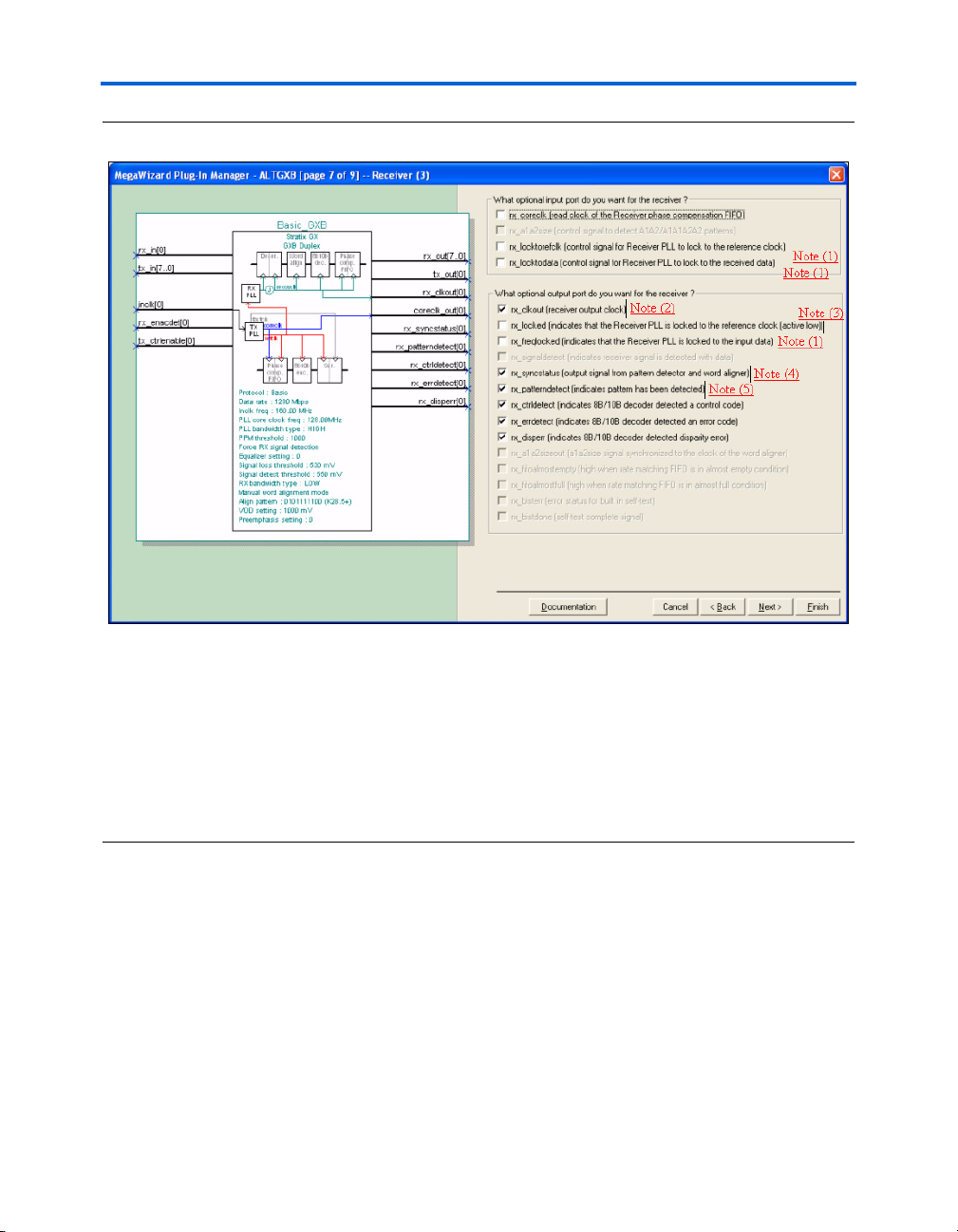
Basic Mode MegaWizard Plug-In
Figure 3–29. MegaWizard Plug-In Manager - ALTGXB (Page 7 of 9) - Receiver (3) Notes (1)–(5)
Notes to Figure 3–29:
(1) For more information, refer to the Stratix GX Analog Description chapter.
(2) The rx_clkout signal is a recovered clock output from individual receiver channels. One rx_clkout signal is
available per channel.
(3) The rx_locked signal is an active low signal that indicates that the receiver PLL is phase locked to the reference
clock. In data mode, this signal might be deasserted because the phase is being locked to the data and not the
reference clock.
(4) The rx_syncstatus signal indicates the status of the word aligner. Refer to the section “Word Aligner” on
page 3–2 for more information.
(5) The rx_patterndetect signal is an active high signal that signifies that the comma appears in the current byte
boundary of the incoming data stream.
3–34 Altera Corporation
Stratix GX Transceiver User Guide January 2005
Page 81

Figure 3–30. MegaWizard Plug-In Manager - ALTGXB (Page 8 of 9) - Transmitter Note (1)
Basic Mode
Notes to Figure 3–30:
(1) For more information, refer to the Stratix GX Analog Description chapter.
Altera Corporation 3–35
January 2005 Stratix GX Transceiver User Guide
Page 82

Basic Mode MegaWizard Plug-In
Figure 3–31. MegaWizard Plug-In Manager - ALTGXB (Page 9 of 9) - Summary
3–36 Altera Corporation
Stratix GX Transceiver User Guide January 2005
Page 83

4. SONET Mode
Introduction
One of the most common serial backplanes in the communications or
telecom area is the SONET/SDH interface. For SONET/SDH
applications the synchronous transport signal STS-48 and Synchronous
Transport Module -16 (STM -16) are becoming popular SONET
backplanes.
Transceiver blocks provide an implementation of SONET/SDH
backplanes. The serial data range over 40'' of FR4 printed circuit board
support a STS-12/STS-48 and STS-192 standards data range. You can
implement many functions associated with SONET/SDH processing.
SONET/SDH backplanes are not designed to a specific standard because
different telecom manufacturers have developed their own proprietary
buses. The backplane transceiver in a SONET/SDH application requires
two types of features: protocol-specific functions and electrical features.
Transceiver blocks provide both of these features to a limited extent. One
example is the protocol feature using A1A2 or A1A1A2A2 for word
alignment.
SONET mode supports a subset of the transceiver blocks to allow for
customizable configuration. The channel aligner, rate matcher, and the
8B/10B encoder/decoder features are not available in this mode. This
chapter describes the supported digital architecture, clocking schemes,
and software implementation in SONET mode. Figure 4–1 shows a block
diagram of a transceiver channel configured in SONET mode.
®
Stratix
GX devices offer the following SONET/SDH features:
■ Serial data rate range from 614 Mbps to 3.1875 Gbps (non-encoded)
■ Input reference clock range from 38.375 to 650 MHz
■ Supports parallel interface width of 8 or 16 bits
■ Word aligner supports 16-bit or bit-slip mode
Altera Corporation 4–1
January 2005
Page 84
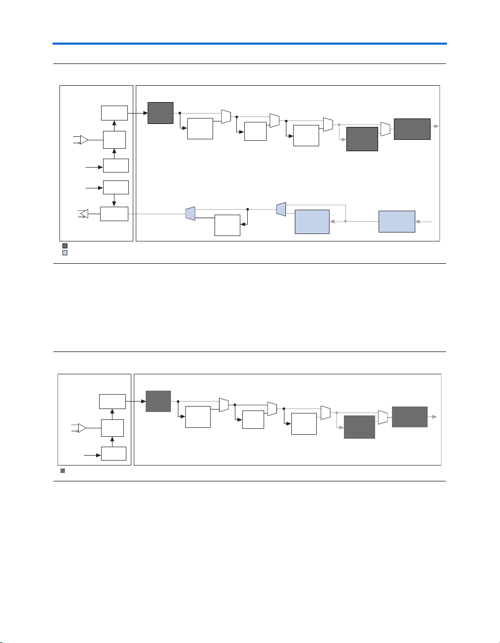
SONET Mode Receiver Architecture
Figure 4–1. Block Diagram of Transceiver Channel Configured in SONET Mode
Digital SectionAnalog Section
Deserializer
Clock
Recovery
Unit
Reference
Clock
Reference
Clock
Receiver
Transmitter
Receiver
PLL
Transmitter
PLL
Serializer
SONET Mode
Word
Aligner
Channel
Aligner
8B/10B
Encoder
Rate
Matcher
8B/10B
Decoder
Serializer
Byte
Figure 4–2 shows the digital components of the Stratix GX receiver that
are active in SONET mode.
Receiver
Architecture
Figure 4–2. Block Diagram of Receiver Digital Components in SONET Mode
Digital SectionAnalog Section
Byte
Deserializer
Compensation
FIFO Buffer
Phase
Compensation
FIFO Buffer
Phase
Word
Aligner
Channel
Aligner
Rate
Matcher
8B/10B
Decoder
Byte
Deserializer
Phase
Compensation
FIFO Buffer
Reference
Clock
Receiver
Deserializer
Clock
Recovery
Unit
Receiver
PLL
Word Aligner
For embedded clocking schemes, the clock is recovered from the
incoming data stream based on transition density of the data. This feature
eliminates the need to factor in receiver skew margins between the clock
and data. However, with this clocking methodology, the word boundary
of the re-timed data can be altered. Stratix GX transceivers offer an
4–2 Altera Corporation
Stratix GX Transceiver User Guide January 2005
Page 85

embedded word alignment circuit to use in conjunction with the pattern
detector to align the word boundary of the re-timed data to a specified
comma. In SONET mode, this embedded circuit is configured to manual
alignment mode consisting of 16-bit and bit-slip modes.
The word aligner is composed of a pattern detector, manual alignment
controller, bit-slipper circuitry, and synchronization state machines.
Depending on the configuration, these components work in conjunction
with or independently of one another. The word aligner cannot be
bypassed, but if the rx_enacdet signal is held low, the word aligner
does not alter the word boundary. Figure 4–3 shows the various
components of the word aligner in SONET mode. The functionality is
described in the following sections.
Figure 4–3. Stratix GX Word Aligner Components
Word Aligner
SONET Mode
A1A2
Mode
Pattern
Detector
SONET
Mode
Manual
Alignment Mode
A1A1A2A2
Mode
Bit-slip
Mode
A1A2
Mode
SONET
Mode
A1A1A2A2
Pattern Detector Module
The pattern detector matches the comma to the current byte-boundary, as
specified in the MegaWizard® Plug-In Manager. If the comma is found,
the optional rx_patterndetect signal is asserted for the duration of
one clock cycle to signify that the comma exists in the current word
boundary. The pattern detector module only indicates that the signal
exists and does not modify the word boundary. Modification of the word
boundary is discussed later in the word alignment and synchronization
sections.
Mode
Altera Corporation 4–3
January 2005 Stratix GX Transceiver User Guide
Page 86

SONET Mode Receiver Architecture
Manual SONET Alignment Mode (2 Consecutive 8-bit Characters
(A1A2) or 4 Consecutive 8-bit Characters (A1A1A2A2)
The 2 consecutive 8-bit characters, A1A2 SONET Section Overhead
Framing Bytes, are used as the comma in 16-bit pattern mode.
The 16-bit comma is specified in the MegaWizard Plug-In Manager. The
comma has the bit orientation of [MSB..LSB]. A1 represents the least
significant byte, which consist of bits [7..0], and A2 represents the most
significant byte consisting of bits [15..8]. The comma, or alignment
pattern, must be specified as [A2,A1] in the MegaWizard Plug-In
Manager. If “Flip Word Alignment bits” is selected, the ordering of the
alignment pattern is [LSB..MSB] for the bit ordering and [A1, A2] for the
byte ordering. Only the positive disparity of the comma is detected in the
mode. Ta bl e 4 –1 shows several word alignment patterns based on
different bit transmission orders and whether the receiver word
alignment bit flip option is checked. The bit transmission order assumes
that if double width mode is used, the LSB is transmitted first, followed
by the MSB.
Table 4–1. Word Alignment Patterns for SONET Mode
Bit Transmission Order
(at the Source)
MSB to LSB On 1111011000101000
MSB to LSB Off 0001010001101111
LSB to MSB Off 0010100011110110
Word Alignment Bit Flip Word Alignment Pattern
(hex F628)
(hex 146F)
(hex 28F6)
In SONET mode, the word aligner either aligns to two consecutive 8-bit
characters (A1A2) or four consecutive 8-bit characters (A1A1A2A2). The
rx_a1a2size[] signal differentiates between the 2 and 4 consecutive
modes. The word aligner aligns to the A1A2 pattern when the
rx_a1a2size[] is held low, or to the A1A1A2A2 when
rx_a1a2size[] is high. If the optional rx_a1a2size signal is not
selected, the word aligner defaults to the A1A2 mode. An optional signal,
rx_a1a2sizeout[], can also be enabled to send the state of the
rx_a1a2[] signa l as seen by the word aligner in to the d evice logi c array.
The value of the signal is forwarded to the device, along with the byte that
was in the word aligner when the rx_a1a2size[] signal was sampled.
4–4 Altera Corporation
Stratix GX Transceiver User Guide January 2005
Page 87

SONET Mode
In SONET mode, the byte boundary is locked after the first comma is
detected, and the boundary is aligned after the rising edge of the
rx_enacdet[] signal. If the byte boundary changes the
rx_enacdet[] signal must be deasserted and reasserted to reset the
alignment circuit. This feature is valuable in SONET because the data is
scrambled and not encoded. The comma can exist across byte boundaries
and can trigger a false re-alignment. In SONET, the byte boundary must
be aligned and locked at the beginning of a SONET frame, because the
A1A2 comma resides in the framing section at the beginning of the
transport overhead.
Because the SONET frame is a set size, the occurrence of the A1A2
framing bytes is anticipated. The actual A1A2 framing bytes are checked
with a counter (A1A2 framing bytes occur every 125 µs based on an STS1 Frame and a rate of 51.84 Mbps).
As stated earlier, at the rising edge of the rx_enacdet[], the word
aligner locks onto the first comma detected. In this scenario, the
rx_patterndetect[] is asserted for one clock cycle to signify that the
comma has been aligned. Also, the rx_syncstatus[] signal is asserted
for a clock cycle to signify that the word boundary has been
synchronized. After the word boundary has been locked, regardless of
whether the rx_enacdet[] is held high or low, the rx_syncstatus[]
signal asserts itself for one clock cycle whenever the comma is detected
across a different byte boundary. The rx_syncstatus[] operates in this
re-synchronization state until a rising edge is detected on the
rx_enacdet[].
Figure 4–4 shows an example of how the word aligner signals interact in
SONET alignment mode for an A1A2 pattern. In this example, a SONET
A1A2 Framing pattern is used (16'b0001010001101111). In this case,
the A1 is represented by 8'b01101111, and A2 is represented by
8'b00010100.
Altera Corporation 4–5
January 2005 Stratix GX Transceiver User Guide
Page 88

SONET Mode Receiver Architecture
Figure 4–4. Word Aligner Symbols Interacting in SONET A1A2 Manual Alignment Mode
rx_recovclockout
rx_word_align_out
rx_enacdet
rx_patterndetect
rx_syncstatus
rx_a1a2size
n n+1 n+2 n+3 n+4 n+5
01101111 00010100 11111111 0110111100000001 0001010001000110
The rx_a1a2size signal is held low. This low signal sets the SONET
alignment mode to A1A2. Because rx_enacdet is toggled high at
time n, the aligner locks to the boundary of the next present comma.
Additionally, the A1 comma appears on the rx_word_align_out port
during this period. At time n+1, the A2 comma appears on the
rx_word_align_out port. Because the comma exists, the
rx_patterndetect and rx_syncstatus signals are asserted for one
clock cycle to signify that the A1A2 comma has been detected and that the
word boundary has been locked. The A1A2 comma appears again across
word boundaries during periods n+2, n+3, and n+4. The rx_enacdet
signal is held high, but the word aligner does not re-align the byte
boundary. Instead, the rx_syncstatus signal is asserted for one clock
cycle to signify a re-synchronization condition. You must deassert and
reassert the rx_enacdet signal to re-trigger the word aligner. The next
transition occurs at time n+5, where rx_enacdet is deasserted and the
A1 pattern is present on the rx_word_align_out por t. At time n+6, t he
A2 pattern is present on the rx_word_align_out port. The word
aligner then asserts the rx_patterndetect signal for one clock cycle to
flag the detection of the comma on the current word boundary.
n+6
Manual Bit-Slipping Alignment Mode
Word alignment is achieved by enabling the manual bit-slip option in the
MegaWizard Plug-In Manager. With this option enabled, the transceiver
can shift the word boundary by one bit in every parallel clock cycle. Bits
are shifted from the MSB to LSB direction. This shift occurs every time the
bit-slipping circuitry detects a rising edge of the rx_bitslip[] signal.
Each time a bit is slipped, the bit that arrived at the receiver earlier is
skipped. When the word boundary matches what is specified as the
4–6 Altera Corporation
Stratix GX Transceiver User Guide January 2005
Page 89

SONET Mode
comma, the rx_patterndetect[] signal is asserted for one clock
cycle. You must implement the logic in the device logic array to control
the bit-slip circuitry.
This scheme is useful if the comma changes dynamically when the
Stratix GX device is in user mode. Because the controller is implemented
in the logic array, a custom controller can be built to dynamically change
the comma without needing to reprogram the Stratix GX device. The
pattern detect circuitry matches only the pattern that is specified in the
MegaWizard Plug-In Manager and is not dynamically adjustable.
Figure 4–5 shows an example of how the word aligner signals interact in
the manual bit-slip alignment mode. In this example, 8'b00111100 is
specified as the comma, and an 8'b11110000 value is held at the rx_in
port. Every rising edge on the rx_bitslip port causes the
rx_word_align_out data to shift one bit from the MSB to the LSB. At
time n+2, the 8'b11110000 data is shifted to a value of 8'b01111000.
At this state the rx_patterndetect is held low, because the specified
comma does not exist in the current word boundary. The rx_bitslip is
disabled at time n+3 and re-enabled at time n+4. The output of the
rx_word_align_out now matches the specified comma, so the
rx_patterndetect is asserted for one clock cycle. At time n+5, the
rx_patterndetect is still asserted because the comma still exists in the
current word boundary. Finally, at time n+6, the rx_word_align_out
boundary is shifted again and the rx_patterndetect signal is
deasserted to signify that the word boundary does not contain the
comma.
Figure 4–5. Word Aligner Symbols Interacting in Manual Bit-Slip Mode
n n+1 n+2 n+3 n+4 n+5 n+6
rx_recovclockout
rx_in
rx_word_align_out
rx_bitslip
rx_patterndetect
Altera Corporation 4–7
January 2005 Stratix GX Transceiver User Guide
11110000
11110000
01111000
00111100
00011110
Page 90

SONET Mode Receiver Architecture
Byte Deserializer
The byte deserializer module further reduces the speed that the FPGA
logic array must achieve in order to meet performance. The possible
division factors are 8 and 16. This requirement results in a byte or double
byte data width in the PLD logic array.
In SONET mode, the maximum output bus width is 22 bits. If the input
includes data and control signals, the data and the control signals are
deserialized to include double the data bits and 2 bits of each control
signal, one for the MSB and one for the LSB. This case is shown when in
SONET mode where the inputs to the Byte Deserializer are
datain[7..0], rx_syncstatus, rx_patterndetect, and
rx_a1a2sizeout. These total 11 input signals feeding the byte
deserializer and 22 output signals are fed to the FPGA logic array. The
signals are sent into the logic array as two 11-bit buses. The aggregate
bandwidth does not change by use of the Byte Deserializer because the
logic array data width is doubled.
Figure 4–6 demonstrates input and output signals of the byte deserializer
when deserializing an 8-bit data input to 16-bits. In this case, the finishing
alignment pattern A2 (00010100) shown as 'B' is located in the MSB of the
16-bit output and this is reflected with patterndetect [1] going high.
The output of the byte deserializer is BA, DC, FE, and so on. This example
assumes that the word alignment bit-flip option is unchecked (OFF), and
that the transmitter and receiver bit-flip option is checked (ON) to adhere
to the MSB transmitted first option.
Figure 4–6. Receiver Byte Deserializer in 8/16-Bit Mode With Finishing Alignment Pattern in MSB
inclk
F
11001100
DC
data_in[7..0]
data_out[15..0]
patterndetect[0]
patterndetect[1]
A
00010100 1100011001101111
xxxxxxxxxxxxxxxxxxxx
B
C
0001010001101111
BA
D
11110001
E
10101010
1111000111000110
4–8 Altera Corporation
Stratix GX Transceiver User Guide January 2005
Page 91

SONET Mode
Figure 4–7 demonstrates the alternate case of the finishing alignment
pattern found in the LSB of the 16-bit output. Correspondingly
patterndetect[0] goes high. In this case, the output is BA, DC, FE,
and so on.
Figure 4–7. Receiver Byte Deserializer in 8/16-Bit Mode with Finishing Alignment Pattern in LSB
inclk
data_in[7..0]
data_out[15..0]
patterndetect[0]
patterndetect[1]
A
xxxxxxxx01101111
B
11000110 1111000100010100
C
11000110 00010100
BA
D
10101010
E
11001100
DC
10101010 11110001
11111000
F
If necessary, you might implement logic to perform byte position
alignment once data enters the logic array, as seen in Figure 4–8. In this
example, the byte position selection logic determines the proper byte
position based on the pattern detect signal.
Altera Corporation 4–9
January 2005 Stratix GX Transceiver User Guide
Page 92

SONET Mode Receiver Architecture
Figure 4–8. Receiver Byte Deserializer Data Recovery in Logic Array
Gigabit Transceiver Block Logic Array
Phase
Compensation
FIFO
Buffer
rx_out[19..10]
10
rx_out[9..0]
10
DQ
DQ
rx_out_post[19..10]
10
10
{rx_out[9..0], rx_out_post[19..10]}
rx_out_post[9..0]
10
Byte Boundary
Selection Logic
rx_out_post[19..0]
10
rx_out_align[19..0]
20
Receiver Phase Compensation FIFO Module
The receiver phase compensation FIFO module is located at the FPGA
logic array interface in the receiver block and is four words deep. The
FIFO module compensates for the phase difference between the clock in
the FPGA and the operating clocks in the transceiver block.
In SONET mode, the write port is clocked by the recovered clock from the
CRU. The rate of this clock is reduced by half if the byte deserializer is
used. The read clock is clocked by rx_coreclk.
You can select rx_coreclk as an optional receiver input port that can
also accept a clock supply. The clock that feeds the rx_coreclk must be
derived from the rx_clkout of its associated receiver channel. The
receiver phase compensation FIFO buffer can only account for phase
differences.
In SONET mode, if you do not select the rx_clkout port, the read clock
of the receiver phase compensation FIFO module, clocked by
rx_coreclk, is fed by rx_clkout. An FPGA global clock, regional
clock, or fast regional clock resource is required to make the connection
4–10 Altera Corporation
Stratix GX Transceiver User Guide January 2005
Page 93

SONET Mode
for the read clock. Refer to “SONET Mode Channel Clocking” on
page 4–12 or the block diagram in the MegaWizard Plug-In Manager for
more information on the clock structure in a particular mode.
The Receiver Phase Compensation FIFO module is always used and
cannot be bypassed.
SONET Mode Transmitter Architecture
Figure 4–9 shows a diagram of the digital components of the transmitter.
The rest of this section describes the active components of the transmitter,
which are the phase compensation FIFO buffer and the byte serializer.
The 8B/10B decoder is not active during SONET mode.
Figure 4–9. Block Diagram of the Transmitter Digital Components in SONET Mode
Digital SectionAnalog Section
Reference
Clock
Transmitter
Transmitter
PLL
Serializer
8B/10B
Encoder
Byte
Serializer
Transmitter Phase Compensation FIFO Buffer
The transmitter phase compensation FIFO buffer is located at the FPGA
logic array interface in the transmitter block and is four words deep. The
phase compensation FIFO module compensates for the phase difference
between the clock in the FPGA and the operating clocks in the transceiver
block.
The read port of the phase compensation FIFO buffer is clocked by the
transmitter PLL clock. The write clock is clocked by tx_coreclk. You
can select the tx_coreclk as an optional transmitter input port to
supply a clock to. In this case, you must ensure that there is no frequency
difference between the tx_coreclk and the transmitter PLL clock. The
transmitter phase compensation FIFO module can only account for phase
differences.
Phase
Compensation
FIFO Buffer
If the tx_coreclk is not selected as an optional input transmitter port,
tx_coreclk is fed by coreclk_out. This connection occurs using the
logic array routing. In this case, the software defaults to using an FPGA
global clock, regional clock, or fast regional clock resource.
Altera Corporation 4–11
January 2005 Stratix GX Transceiver User Guide
Page 94

SONET Mode Clocking
The Transmitter Phase Compensation FIFO module is always used and
cannot be bypassed. The input to the Transmitter Phase Compensation
FIFO module is the data from the FPGA logic array.
Byte Serializer
In SONET mode, the Byte Serializer in the transmitter block takes in a
16-bit input from the phase compensation FIFO module and serializes it
to 8 bits. It transmits the least significant byte to the most significant byte.
The transmitter digital reset must always be used to reset the Byte
Serializer FIFO module pointers whenever an unknown state is
encountered, for example, during periods when the transmitter PLL loses
lock. Refer to Chapter 8, Reset Control and Power Down, for further
details on the reset sequence.
Figure 4–10 demonstrates input and output signals of the byte serializer
when serializing a 16 bit input to 8 bits. The tx_in[] signal is the
input from the FPGA logic array that has already passed through the
Transmitter Phase Compensation FIFO module.
Figure 4–10. Transmitter Byte Serializer in 8- to 16-Bit Mode
D1
datain[15..0]
0001010001101111
1100011011110001 1010101010110011
D2 D3
dataout[7..0]
xxxxxxxx 01101111xxxxxxxx 00010100 1100011011110001
MSBLSB
D1
LSB MSB
D2
The LSB is transmitted before the MSB in the transmitter byte serializer.
Figure 4–10 shows the order of data transmitted. For the input of D1, the
output is D1LSB and then D1MSB. The byte serializer is selected in the
MegaWizard Plug-In Manager when a 16-bit channel width is selected.
SONET Mode
Clocking
SONET Mode Channel Clocking
This section covers describes the internal clocking and the external clocks
of the transceiver in SONET mode. By default, the MegaWizard Plug-In
Manager parameterizes the altgxb megafunction with the clock
configuration shown in Figure 4–11.
4–12 Altera Corporation
Stratix GX Transceiver User Guide January 2005
Page 95

Figure 4–11. Default Configuration of altgxb in SONET Mode
SONET Mode
In Figure 4–11, the altgxb megafunction is configured so that the train
receiver PLL with transmitter PLL is enabled. The transmitter PLL is fed
from an inclk port, which can be fed from a dedicated REFCLKB, Global
clock, Regional clock, or Fast Regional clock source. The receiver logic is
clocked by the recovered clock from the clock recovery unit, rx_clkout.
This recovered clock is also fed into the FPGA so that, in a multi-crystal
environment, some level of clock domain decoupling can be
implemented to interface with a system clock. On the transmitter channel,
the output of the transmitter PLL, coreclk_out, is sent into the logic
array and also loops back to clock the write side of the transmit phase
compensation FIFO module.
The train receiver PLL CRU clock from the transmitter PLL feature can be
disabled in the altgxb MegaWizard
Plug-In. Deselecting this option
enables an additional rx_cruclk input reference clock port for the
receiver PLL. This feature supports additional multiplication factors for
the receiver PLL and allows for the separation of receiver and transmitter
reference clocks. This separation is required if the output reference clock
frequency from the transmitter PLL exceeds the 325 MHz phase
Altera Corporation 4–13
January 2005 Stratix GX Transceiver User Guide
Page 96

SONET Mode Clocking
frequency detector of the receiver PLL. For more information on this
feature, refer to the Stratix GX Analog Description chapter. This
configuration is shown in Figure 4–12.
If double width is used (16-bit bus) and the data rate is above 2,600 Mbps,
the trained receiver PLL clock from the transmitter PLL must be turned
off, because the output clock from the transmitter PLL exceeds the 325MHz limit on the receiver PLL input clock, if the input clock is fed from
any non-REFCLKB pin. REFCLKB pins have a 650-MHz limit.
Figure 4–12. altgxb Megafunction in SONET Mode With Train Receiver CRU From Transmitter PLL Disabled
This configuration contains an independent rx_cruclk, which feeds the
receiver PLL reference clock. This input clock port is only available when
the receiver PLL is not trained by the transmitter PLL. One rx_cruclk
is associated with a channel. If four channels are active, there are four
rx_cruclks.
The rx_clkout is the recovered clock from the associated receiver
channel. An rx_clkout is available for each receiver channel that is
used. This clock is used to clock the write port of a rate matching FIFO
module. The read port of the FIFO module is clocked by the
coreclk_out or PLD clock.
4–14 Altera Corporation
Stratix GX Transceiver User Guide January 2005
Page 97

SONET Mode
The coreclk_out is the output from the transmitter PLL. A
coreclk_out is available for each transceiver block that is used. Altera
recommends clocking the logic that is feeding the transmitter with this
clock.
The read clock of the receiver phase compensation FIFO module and the
write clock of the transmitter phase compensation FIFO module are
optionally enabled to manually feed in a clock from the FPGA logic array.
You use these options to optimize the global clock usage. For instance, if
all transmitter channels between transceiver blocks are from a common
clock domain, the transceiver instantiations use a total of one global
resource clock versus one global per transceiver block, if the
tx_coreclk option is not enabled.
The same situation can be optimized for the receiver channels in a single
crystal synchronous system with the rx_coreclk. Even in a system that
is based on a single crystal, the recovered clock can still become
asynchronous to the system clock during initialization or long run
lengths. As a result, the pointers of the Receiver Phase Compensation
FIFO module might overlap and fail to function correctly. In situations
where there are long run lengths or no data transmissions, these FIFO
modules must be reset by the rxdigitalreset signal.
In multi-crystal environments, individual recovered clocks must drive
®
the read clock of the phase compensation FIFO module. The Quartus
II
software does this by default, and you do have to manually make this
connection. The rx_coreclk and tx_coreclk must be frequency
matched with their respective read and write ports. The phase
compensation FIFO module can only correct for phase, not frequency
differences. Figure 4–13 shows the clock configuration with these
optional input ports enabled.
®
Altera Corporation 4–15
January 2005 Stratix GX Transceiver User Guide
Page 98

SONET Mode Clocking
Figure 4–13. altgxb in SONET Mode With rx_coreclk & tx_coreclk Enabled
For reference, the various input and output clock ports are listed in
Table 4–2.
Table 4–2. List of Clocking Input & Output Ports Available in SONET Mode
(Part 1 of 2)
Clock Port Description
rx_cruclk
inclk
coreclk_out
Input Input to CRU available as
a port when CRU is not
trained by the transmitter
PLL.
Input Input to the transmitter
PLL, available as a port
when the transmitter PLL
is instantiated.
Output Output clock from the
transmitter PLL
equivalent to
TX_PLL_CLK. Available
as a port if the transmitter
PLL is used.
4–16 Altera Corporation
Stratix GX Transceiver User Guide January 2005
Page 99

SONET Mode
Table 4–2. List of Clocking Input & Output Ports Available in SONET Mode
(Part 2 of 2)
Clock Port Description
rx_clkout
Output Output clock from
transceiver. In this mode,
rx_clkout is the
recovered clock of the
respective channel.
tx_coreclk
Input Clocks the write port of
transmitter phase
compensation FIFO
module. Available as an
optional port in the
Quartus II MegaWizard®
Plug-In Manager. Must
be frequency matched to
tx_pll_clk. If not
available as a port, this is
fed by
coreclk_out
through logic array
routing.
rx_coreclk
Input Clocks read port of
receiver phase
compensation FIFO
module. Available as an
optional port in the
Quartus II MegaWizard
Plug-In Manager. If not
available as a port, this is
fed by
rx_clkout
through logic array
routing.
SONET Mode Inter-Transceiver Block Clocking
This section provides guidelines for using transceiver interface clocking
between the FPGA logic array and transceiver channels when multiple
transceiver blocks are active. Depending on each mode supported by
Stratix GX devices, each transceiver block contains different
transceiver-to-FPGA interface clocking. Different input and output clocks
are available based on the options provided by the Quartus II
MegaWizard Plug-In Manager’s built-in functions. The number of
supported channels varies based on which Stratix GX device you select.
Because of the various configurations of input and output clocks,
consider the clocking schemes between inter-transceiver blocks carefully
to prevent problems later in the design cycle.
Altera Corporation 4–17
January 2005 Stratix GX Transceiver User Guide
Page 100

SONET Mode Clocking
One of the clocking interfaces to consider while designing with Stratix GX
devices is the transceiver-to-FPGA interface. This clocking scheme is
further classified as the FPGA-to-transmitter channel and the
FPGA-to-receiver channel to the PLD.
In SONET mode, the read port of the transmitter phase compensation
FIFO module is either clocked by the coreclk_out or by the
tx_coreclk signal. The constraint on using tx_coreclk is that the
clock must be frequency locked to the read clock of the transmitter phase
compensation FIFO module. Synchronous data transfers for a
multi-transceiver block configuration are accomplished by using the
tx_coreclk port. The tx_coreclk of multi-transceiver blocks are
connected to a common clock domain either from a single coreclk_out
signal or from an FPGA system clock domain. This scheme is shown in
Figure 4–14.
4–18 Altera Corporation
Stratix GX Transceiver User Guide January 2005
 Loading...