

Page 1

Stratix GX Device Handbook, Volume 1
101 Innovation Drive
San Jose, CA 95134
(408) 544-7000
www.altera.com
SGX5V1-1.2
Page 2

Copyright © 2006 Altera Corporation. All rights reserved. Altera, The Programmable Solutions Company, the stylized Altera logo, specific device designations, and all other words and logos that are identified as trademarks and/or service marks are, unless noted otherwise, the trademarks and
service marks of Altera Corporation in the U.S. and other countries. All other product or service names are the property of their respective holders. Altera products are protected under numerous U.S. and foreign patents and pending applications, maskwork rights, and copyrights. Altera warrants
performance of its semiconductor products to current specifications in accordance with Altera's standard warranty, but reserves the right to make
changes to any products and services at any time without notice. Altera assumes no responsibility or liability arising out of the application or use of any information, product, or service described herein except as
expressly agreed to in writing by Altera Corporation. Altera customers are advised to obtain the latest version of device specifications before relying on any published information and before placing orders for
products or services.
ii Altera Corporation
Page 3

Contents
Chapter Revision Dates .......................................................................... vii
About This Handbook .............................................................................. ix
How to Contact Altera ............................................................................................................................. ix
Typographic Conventions ....................................................................................................................... ix
Section I. Stratix GX Device Family Data Sheet
Revision History ....................................................................................................................... Section I–2
Chapter 1. Introduction to the Stratix GX Device Data Sheet
Overview ................................................................................................................................................. 1–1
Features ................................................................................................................................................... 1–1
High-Speed I/O Interface Functional Description ........................................................................... 1–4
FPGA Functional Description .............................................................................................................. 1–5
Chapter 2. Stratix GX Transceivers
Transmitter Path ............................................................................................................................... 2–5
Receiver Path ................................................................................................................................... 2–13
Loopback Modes ............................................................................................................................ 2–26
BIST (Built-In Self Test) ................................................................................................................. 2–28
Stratix GX Clocking ........................................................................................................................ 2–30
Other Transceiver Features ................................................................................................................ 2–37
Individual Power-Down & Reset for the Transmitter & Receiver .......................................... 2–37
Voltage Reference Capabilities ..................................................................................................... 2–38
Hot-Socketing Capabilities ........................................................................................................... 2–39
Applications & Protocols Supported with Stratix GX Devices ..................................................... 2–39
Stratix GX Example Application Support ................................................................................... 2–39
High-Speed Serial Bus Protocols .................................................................................................. 2–40
Chapter 3. Source-Synchronous Signaling With DPA
Introduction ............................................................................................................................................ 3–1
Stratix GX I/O Banks ....................................................................................................................... 3–1
Principles of SERDES Operation .................................................................................................... 3–1
DPA Block Overview ....................................................................................................................... 3–5
DPA Operation ............................................................................................................................... 3–10
Altera Corporation iii
Page 4

Contents
Chapter 4. Stratix GX Architecture
Logic Array Blocks ................................................................................................................................ 4–1
LAB Interconnects ............................................................................................................................ 4–1
LAB Control Signals ......................................................................................................................... 4–2
Logic Elements ....................................................................................................................................... 4–3
LUT Chain & Register Chain .......................................................................................................... 4–5
addnsub Signal ................................................................................................................................. 4–5
LE Operating Modes ........................................................................................................................ 4–5
Clear & Preset Logic Control ........................................................................................................ 4–10
MultiTrack Interconnect ..................................................................................................................... 4–11
TriMatrix Memory ............................................................................................................................... 4–18
Memory Modes ............................................................................................................................... 4–19
Parity Bit Support ........................................................................................................................... 4–21
Shift Register Support .................................................................................................................... 4–21
Memory Block Size ......................................................................................................................... 4–22
Independent Clock Mode .............................................................................................................. 4–40
Input/Output Clock Mode ........................................................................................................... 4–42
Read/Write Clock Mode ............................................................................................................... 4–44
Single-Port Mode ............................................................................................................................ 4–45
Digital Signal Processing Block ......................................................................................................... 4–46
Multiplier Block .............................................................................................................................. 4–52
Adder/Output Blocks ................................................................................................................... 4–56
Modes of Operation ....................................................................................................................... 4–59
DSP Block Interface ........................................................................................................................ 4–65
PLLs & Clock Networks ..................................................................................................................... 4–68
Global & Hierarchical Clocking ................................................................................................... 4–68
Enhanced & Fast PLLs ................................................................................................................... 4–76
Enhanced PLLs ............................................................................................................................... 4–82
Fast PLLs .......................................................................................................................................... 4–93
I/O Structure ........................................................................................................................................ 4–96
Double-Data Rate I/O Pins ......................................................................................................... 4–103
External RAM Interfacing ........................................................................................................... 4–107
Programmable Drive Strength ................................................................................................... 4–110
Open-Drain Output ...................................................................................................................... 4–111
Slew-Rate Control ........................................................................................................................ 4–112
Bus Hold ........................................................................................................................................ 4–112
Programmable Pull-Up Resistor ................................................................................................ 4–113
Advanced I/O Standard Support .............................................................................................. 4–113
Differential On-Chip Termination ............................................................................................. 4–118
MultiVolt I/O Interface ............................................................................................................... 4–120
Power Sequencing & Hot Socketing ............................................................................................... 4–121
IEEE Std. 1149.1 (JTAG) Boundary-Scan Support ........................................................................ 4–122
Chapter 5. Configuration & Testing
SignalTap Embedded Logic Analyzer ................................................................................................ 5–1
Configuration ......................................................................................................................................... 5–1
Operating Modes .............................................................................................................................. 5–1
iv Altera Corporation
Stratix GX Device Handbook, Volume 1
Page 5

Contents
Configuration Schemes ................................................................................................................... 5–2
Partial Reconfiguration .................................................................................................................... 5–3
Remote Update Configuration Modes .......................................................................................... 5–3
Stratix GX Automated Single Event Upset (SEU) Detection ........................................................... 5–7
Custom-Built Circuitry .................................................................................................................... 5–8
Software Interface ............................................................................................................................. 5–8
Temperature-Sensing Diode ................................................................................................................ 5–8
Chapter 6. DC & Switching Characteristics
Operating Conditions ........................................................................................................................... 6–1
Power Consumption ........................................................................................................................... 6–22
Timing Model ....................................................................................................................................... 6–22
Preliminary & Final Timing .......................................................................................................... 6–23
Performance .................................................................................................................................... 6–23
Internal Timing Parameters .......................................................................................................... 6–26
External Timing Parameters ......................................................................................................... 6–35
External I/O Delay Parameters .................................................................................................... 6–44
Maximum Input & Output Clock Rates ...................................................................................... 6–54
High-Speed I/O Specification ........................................................................................................... 6–58
PLL Timing ...................................................................................................................................... 6–62
DLL Jitter ............................................................................................................................................... 6–68
Chapter 7. Reference & Ordering Information
Software .................................................................................................................................................. 7–1
Device Pin-Outs ..................................................................................................................................... 7–1
Ordering Information ........................................................................................................................... 7–1
Altera Corporation v
Stratix GX Device Handbook, Volume 1
Page 6

Contents
vi Altera Corporation
Stratix GX Device Handbook, Volume 1
Page 7

Chapter Revision Dates
The chapters in this book, Stratix GX Device Handbook, Volume 1, were revised on the following dates.
Where chapters or groups of chapters are available separately, part numbers are listed.
Chapter 1. Introduction to the Stratix GX Device Data Sheet
Revised: February 2005
Part number: SGX51001-1.0
Chapter 2. Stratix GX Transceivers
Revised: June 2006
Part number: SGX51002-1.1
Chapter 3. Source-Synchronous Signaling With DPA
Revised: August 2005
Part number: SGX51003-1.1
Chapter 4. Stratix GX Architecture
Revised: February 2005
Part number: SGX51004-1.0
Chapter 5. Configuration & Testing
Revised: February 2005
Part number: SGX51005-1.0
Chapter 6. DC & Switching Characteristics
Revised: June 2006
Part number: SGX51006-1.2
Chapter 7. Reference & Ordering Information
Revised: February 2005
Part number: SGX51007-1.0
Altera Corporation vii
Page 8

Chapter Revision Dates Stratix GX Device Handbook, Volume 1
viii Altera Corporation
Page 9

About This Handbook
This handbook provides comprehensive information about the Altera®
Stratix®GX family of devices.
How to Contact Altera
For the most up-to-date information about Altera products, go to the
Altera world-wide web site at www.altera.com. For technical support on
this product, go to www.altera.com/mysupport. For additional
information about Altera products, consult the sources shown below.
Information Type USA & Canada All Other Locations
Technical support www.altera.com/mysupport/ www.altera.com/mysupport/
(800) 800-EPLD (3753)
(7:00 a.m. to 5:00 p.m. Pacific Time)
Product literature www.altera.com www.altera.com
Altera literature services literature@altera.com literature@altera.com
Non-technical customer
service
FTP site ftp.altera.com ftp.altera.com
Typographic
(800) 767-3753 + 1 408-544-7000
This document uses the typographic conventions shown below.
+1 408-544-8767
7:00 a.m. to 5:00 p.m. (GMT -8:00)
Pacific Time
7:00 a.m. to 5:00 p.m. (GMT -8:00)
Pacific Time
Conventions
Visual Cue Meaning
Bold Type with Initial
Capital Letters
bold type External timing parameters, directory names, project names, disk drive names,
Italic Type with Initial Capital
Letters
Command names, dialog box titles, checkbox options, and dialog box options are
shown in bold, initial capital letters. Example: Save As dialog box.
filenames, filename extensions, and software utility names are shown in bold
type. Examples: f
Document titles are shown in italic type with initial capital letters. Example: AN
75: High-Speed Board Design.
, \qdesigns directory, d: drive, chiptrip.gdf file.
MAX
Altera Corporation ix
Preliminary
Page 10

Typographic Conventions Stratix GX Device Handbook, Volume 1
Visual Cue Meaning
Italic type Internal timing parameters and variables are shown in italic type.
Examples: t
Variable names are enclosed in angle brackets (< >) and shown in italic type.
Example: <file name>, <project name>.pof file.
Initial Capital Letters Keyboard keys and menu names are shown with initial capital letters. Examples:
Delete key, the Options menu.
“Subheading Title” References to sections within a document and titles of on-line help topics are
shown in quotation marks. Example: “Typographic Conventions.”
PIA
, n + 1.
Courier type Signal and port names are shown in lowercase Courier type. Examples: data1,
tdi, input. Active-low signals are denoted by suffix n, e.g., resetn.
Anything that must be typed exactly as it appears is shown in Courier type. For
example:
actual file, such as a Report File, references to parts of files (e.g., the AHDL
keyword
Courier.
1., 2., 3., and
a., b., c., etc.
● • Bullets are used in a list of items when the sequence of the items is not important.
■
v The checkmark indicates a procedure that consists of one step only.
1 The hand points to information that requires special attention.
c
w
r The angled arrow indicates you should press the Enter key.
f The feet direct you to more information on a particular topic.
Numbered steps are used in a list of items when the sequence of the items is
important, such as the steps listed in a procedure.
The caution indicates required information that needs special consideration and
understanding and should be read prior to starting or continuing with the
procedure or process.
The warning indicates information that should be read prior to starting or
continuing the procedure or processes
c:\qdesigns\tutorial\chiptrip.gdf. Also, sections of an
SUBDESIGN), as well as logic function names (e.g., TRI) are shown in
x Altera Corporation
Preliminary
Page 11

Section I. Stratix GX
Device Family Data Sheet
This section provides the data sheet specifications for Stratix® GX
devices. It contains feature definitions of the internal architecture,
configuration information, testing information, DC operating conditions,
and AC timing parameters.
This section includes the following chapters:
■ Chapter 1, Introduction to the Stratix GX Device Data Sheet
■ Chapter 2, Stratix GX Transceivers
■ Chapter 3, Source-Synchronous Signaling With DPA
■ Chapter 4, Stratix GX Architecture
■ Chapter 5, Configuration & Testing
■ Chapter 6, DC & Switching Characteristics
■ Chapter 7, Reference & Ordering Information
Altera Corporation Section I–1
Preliminary
Page 12
Stratix GX Device Family Data Sheet Stratix GX Device Handbook, Volume 1
Revision History
The table below shows the revision history for Chapters 1 through 7.
Chapter(s) Date / Version Changes Made Comments
1 February 2005,
v1.0
2 June 2006, v1.1
February 2005,
v1.0
3 August 2005,
v1.1
4 February 2005,
v1.0
5 February 2005,
v1.0
6 June 2006, v1.2
August 2005,
v1.1
7 February 2005,
v1.0
Initial Release.
● Updated “Serial Loopback” section.
● Updated Figures 2–1 through 2–3.
● Updated Figure 2–13.
● Updated Figures 2–26 and 2–27.
Initial Release.
Added Note (3) to Figure 3-7.
Initial Release.
Initial Release.
● Updated “Operating Conditions” section.
● Updated Table 6–4.
● Updated note 3 in Table 6–6.
● Added note 12 in Table 6–7.
● Updated Figure 6–1.
● Added Figure 6–2.
● Updated Tables 6–13 through 6–16.
Updated Tables 6-7 and 6-50.
Initial Release.
● Changed V
OD
receiver input voltage and
refclkb input voltage in
Table 6–4.
● Changed value for
undershoot during transition
from -0.5 V to -2.0 V in note 3
of Ta bl e 6 – 6.
● Changed value of V
mV to V in Table 6–15.
● Changed unit value of W to
Ω..
to VID for
OCM
from
Section I–2 Altera Corporation
Preliminary
Page 13

SGX51001-1.0
1. Introduction to the
Stratix GX Device Data Sheet
Overview
Features
The Stratix®GX family of devices is Altera’s second FPGA family to
combine high-speed serial transceivers with a scalable, high-performance
logic array. Stratix GX devices include 4 to 20 high-speed transceiver
channels, each incorporating clock data recovery (CDR) technology and
embedded SERDES capability at data rates of up to 3.1875 gigabits per
second (Gbps). These transceivers are grouped by four-channel
transceiver blocks, and are designed for low power consumption and
small die size. The Stratix GX FPGA technology is built upon the Stratix
architecture, and offers a 1.5-V logic array with unmatched performance,
flexibility, and time-to-market capabilities. This scalable,
high-performance architecture makes Stratix GX devices ideal for
high-speed backplane interface, chip-to-chip, and communications
protocol-bridging applications.
■ Transceiver block features are as follows:
● High-speed serial transceiver channels with CDR provides
500-megabits per second (Mbps) to 3.1875-Gbps full-duplex
operation
● Devices are available with 4, 8, 16, or 20 high-speed serial
transceiver channels providing up to 127.5 Gbps of full-duplex
serial bandwidth
● Support for transceiver-based protocols, including 10 Gigabit
Ethernet attachment unit interface (XAUI), Gigabit Ethernet
(GigE), and SONET/SDH
● Compatible with PCI Express, SMPTE 292M, Fibre Channel, and
Serial RapidIO I/O standards
● Programmable differential output voltage (V
), pre-emphasis,
OD
and equalization settings for improved signal integrity
● Individual transmitter and receiver channel power-down
capability implemented automatically by the Quartus
®
II
software for reduced power consumption during non-operation
● Programmable transceiver-to-FPGA interface with support for
8-, 10-, 16-, and 20-bit wide data paths
● 1.5-V pseudo current mode logic (PCML) for 500 Mbps to
3.1875 Gbps
● Support for LVDS, LVPECL, and 3.3-V PCML on reference
clocks and receiver input pins (AC-coupled)
● Built-in self test (BIST)
● Hot insertion/removal protection circuitry
Altera Corporation 1–1
February 2005
Page 14

Features
● Pattern detector and word aligner supports programmable
patterns
● 8B/10B encoder/decoder performs 8- to 10-bit encoding and 10-
to 8-bit decoding
● Rate matcher compliant with IEEE 802.3-2002 for GigE mode
and with IEEE 802-3ae for XAUI mode
● Channel bonding compliant with IEEE 802.3ae (for XAUI mode
only)
● Device can bypass some transceiver block features if necessary
■ FPGA features are as follows:
● 10,570 to 41,250 logic elements (LEs); see Table 1–1
● Up to 3,423,744 RAM bits (427,968 bytes) available without
reducing logic resources
● TriMatrix
™
memory consisting of three RAM block sizes to
implement true dual-port memory and first-in-out (FIFO)
buffers
● Up to 16 global clock networks with up to 22 regional clock
networks per device region
● High-speed DSP blocks provide dedicated implementation of
multipliers (faster than 300 MHz), multiply-accumulate
functions, and finite impulse response (FIR) filters
● Up to eight general usage phase-locked loops (four enhanced
PLLs and four fast PLLs) per device provide spread spectrum,
programmable bandwidth, clock switchover, real-time PLL
reconfiguration, and advanced multiplication and phase
shifting
● Support for numerous single-ended and differential I/O
standards
● High-speed source-synchronous differential I/O support on up
to 45 channels for 1-Gbps performance
● Support for source-synchronous bus standards, including
10-Gigabit Ethernet XSBI, Parallel RapidIO, UTOPIA IV,
Network Packet Streaming Interface (NPSI), HyperTransport
technology, SPI-4 Phase 2 (POS-PHY Level 4), and SFI-4
● Support for high-speed external memory, including zero bus
turnaround (ZBT) SRAM, quad data rate (QDR and QDRII)
SRAM, double data rate (DDR) SDRAM, DDR fast cycle RAM
(FCRAM), and single data rate (SDR) SDRAM
● Support for multiple intellectual property megafunctions from
Altera® MegaCore® functions and Altera Megafunction Partners
Program (AMPPSM) megafunctions
● Support for remote configuration updates
● Dynamic phase alignment on LVDS receiver channels
TM
1–2 Altera Corporation
Stratix GX Device Handbook, Volume 1 February 2005
Page 15
Table 1–1. Stratix GX Device Features
Introduction to the Stratix GX Device Data Sheet
Feature
LEs 10,570 25,660 41,250
Transceiver channels 4, 8 4, 8, 16 8, 20
Source-synchronous channels 22 39 45
M512 RAM blocks (32
M4K RAM blocks (128
M-RAM blocks (4K
Total RAM bits 920,448 1,944,576 3,423,744
Digital signal processing (DSP) blocks 6 10 14
Embedded multipliers (1) 48 80 112
PLLs 4 4 8
Note to Ta b le 1 –1 :
(1) This parameter lists the total number of 9- × 9-bit multipliers for each device. For the total number of 18- × 18-bit
multipliers per device, divide the total number of 9- × 9-bit multipliers by 2. For the total number of 36- × 36-bit
multipliers per device, decide the total number of 9- × 9-bit multipliers by 8.
× 18 bits) 94 224 384
× 36 bits) 60 138 183
×144 bits) 1 2 4
EP1SGX10C
EP1SGX10D
EP1SGX25C
EP1SGX25D
EP1SGX25F
EP1SGX40D
EP1SGX40G
Stratix GX devices are available in space-saving FineLine BGA® packages
(refer to Tables 1–2 and 1–3), and in multiple speed grades (refer to
Table 1–4). Stratix GX devices support vertical migration within the same
package (that is, you can migrate between the EP1SGX10C and
EP1SGX25C devices in the 672-pin FineLine BGA package). See the
Stratix GX device pin tables for more information. Vertical migration
means that you can migrate to devices whose dedicated pins,
configuration pins, and power pins are the same for a given package
across device densities. For I/O pin migration across densities, you must
cross-reference the available I/O pins using the device pin-outs for all
planned densities of a given package type, to identify which I/O pins it
is possible to migrate. The Quartus II software can automatically cross
reference and place all pins for migration when given a device migration
list.
Table 1–2. Stratix GX Package Options & I/O Pin Counts (Part 1
of 2) Note (1)
Device 672-Pin FineLine BGA 1,020-Pin FineLine BGA
EP1SGX10C 362
EP1SGX10D 362
EP1SGX25C 455
Altera Corporation 1–3
February 2005 Stratix GX Device Handbook, Volume 1
Page 16
High-Speed I/O Interface Functional Description
Table 1–2. Stratix GX Package Options & I/O Pin Counts (Part 2
of 2) Note (1)
Device 672-Pin FineLine BGA 1,020-Pin FineLine BGA
EP1SGX25D 455 607
EP1SGX25F 607
EP1SGX40D 624
EP1SGX40G 624
Note to Ta b l e 1 – 2:
(1) The number of I/O pins listed for each package includes dedicated clock pins and
dedicated fast I/O pins. However, these numbers do not include high-speed or
clock reference pins for high-speed I/O standards.
Table 1–3. Stratix GX FineLine BGA Package Sizes
Dimension 672 Pin 1,020 Pin
Pitch (mm) 1.00 1.00
Area (mm
Length
2
)
× width (mm × mm) 27 × 27 33 × 33
729 1,089
Table 1–4. Stratix GX Device Speed Grades
Device 672-Pin FineLine BGA 1,020-pin FineLine BGA
EP1SGX10 -5, -6, -7
EP1SGX25 -5, -6, -7 -5, -6, -7
EP1SGX40 -5, -6, -7
High-Speed I/O
Interface
Functional
Description
The Stratix GX device family supports high-speed serial transceiver
blocks with CDR circuitry as well as source-synchronous interfaces. The
channels on the right side of the device use an embedded circuit
dedicated for receiving and transmitting high-speed serial data streams
to and from the system board. These channels are clustered in a
four-channel serial transceiver building block and deliver high-speed
bidirectional point-to-point data transmissions to provide up to
3.1875 Gbps of full-duplex data transmission per channel. The channels
on the left side of the device support source-synchronous data transfers
at up to 1 Gbps using LVDS, LVPECL, 3.3-V PCML, or HyperTransport
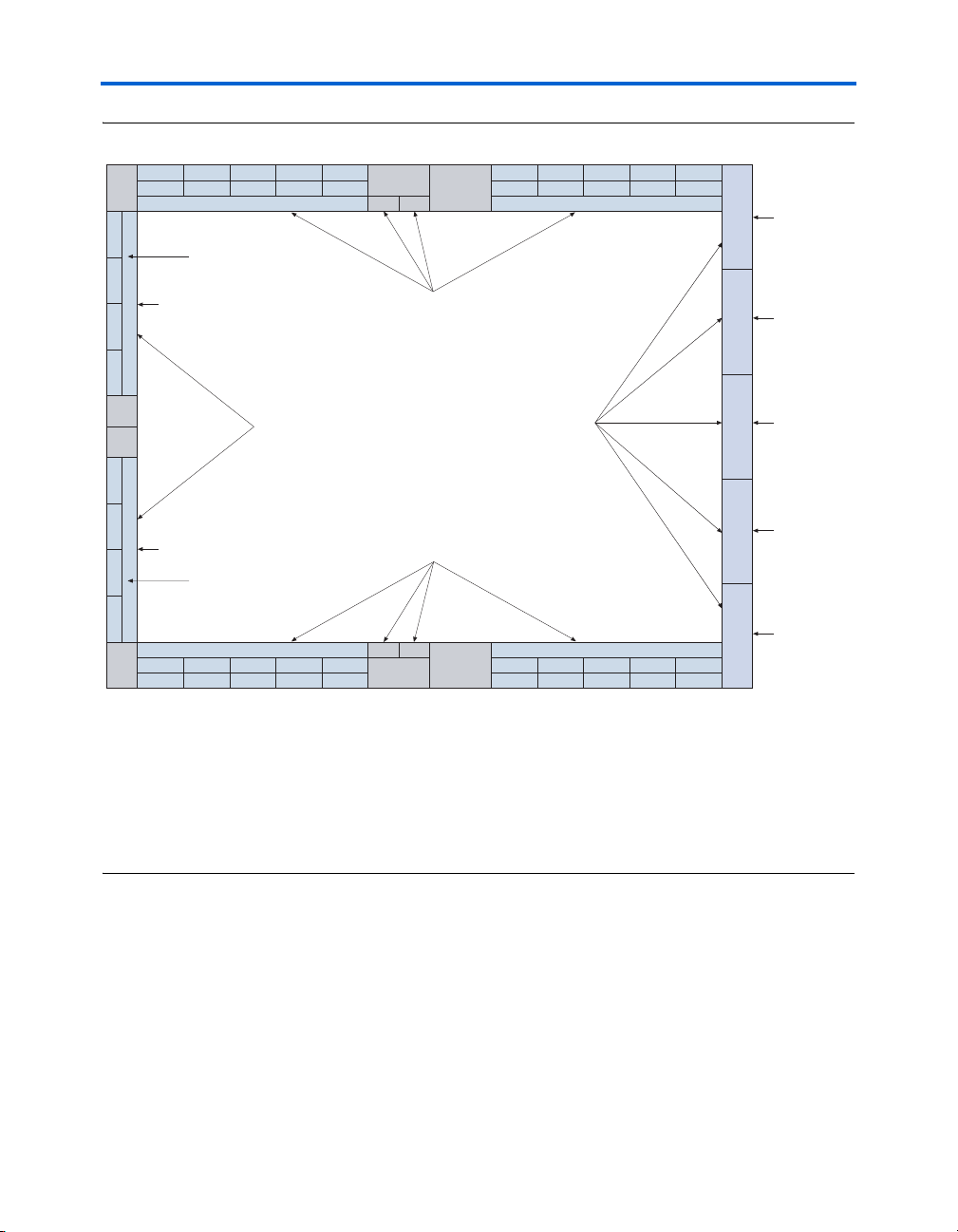
technology I/O standards. Figure 1–1 shows the Stratix GX I/O blocks.
The differential source-synchronous serial interface and the high-speed
serial interface are described in the Stratix GX Transceivers chapter of the
Stratix GX Device Handbook, Volume 1.
1–4 Altera Corporation
Stratix GX Device Handbook, Volume 1 February 2005
Page 17
Introduction to the Stratix GX Device Data Sheet
Figure 1–1. Stratix GX I/O Blocks Note (1)
DQST9 DQST8 DQST7 DQST6 DQST5 DQST4 DQST3 DQST2 DQST1 DQST0
VREF1B3 VREF2B3 VREF3B3 VREF4B3 VREF5B3 VREF1B4 VREF2B4 VREF3B4 VREF4B4 VREF5B4
PLL7
Bank 2
(4)
Bank 3 Bank 4
LVDS, LVPECL, 3.3-V PCML,
and HyperTransport I/O Block
and Regular I/O Pins (3)
PLL5
910
I/O Banks 3, 4, 9 & 10 Support
All Single-Ended I/O Standards (2)
PLL11
I/O Bank 13 (5)
I/O Bank 14 (5)
VREF1B2 VREF2B2 VREF3B2 VREF4B2VREF1B1 VREF2B1 VREF3B1 VREF4B1
PLL1
PLL2
(4)
Bank 1
PLL8
LVDS, LVPECL, 3.3-V PCML,
and HyperTransport I/O Block
and Regular I/O Pins (3)
VREF5B8 VREF4B8 VREF3B8 VREF2B8 VREF1B8 VREF5B7 VREF4B7 VREF3B7 VREF2B7 VREF1B7
DQSB9 DQSB8 DQSB7 DQSB6 DQSB5 DQSB4 DQSB3 DQSB2 DQSB1 DQSB0
I/O Banks 1 and 2 Support All
Single-Ended I/O Standards Except
Differential HSTL Output Clocks,
Differential SSTL-2 Output Clocks,
HSTL Class II, GTL, SSTL-18 Class II,
PCI, PCI-X, and AGP 1
×/2×
I/O Banks 7, 8, 11 & 12 Support
All Single-Ended I/O Standards (2)
11 12Bank 8 Bank 7
PLL6
PLL12
1.5-V PCML (5)
I/O Bank 17 (5)
I/O Bank 16 (5)
I/O Bank 15 (5)
Notes to Figure 1–1:
(1) Figure 1–1 is a top view of the Stratix GX silicon die.
(2) Banks 9 through 12 are enhanced PLL external clock output banks.
(3) If the high-speed differential I/O pins are not used for high-speed differential signaling, they can support all of the
I/O standards except HSTL class I and II, GTL, SSTL-18 Class II, PCI, PCI-X, and AGP 1×/2×.
(4) For guidelines for placing single-ended I/O pads next to differential I/O pads, see the Selectable I/O Standards in
Stratix & Stratix GX Devices chapter of the Stratix GX Device Handbook, Volume 2.
(5) These I/O banks in Stratix GX devices also support the LVDS, LVPECL, and 3.3-V PCML I/O standards on
reference clocks and receiver input pins (AC coupled).
FPGA Functional Description
Stratix GX devices contain a two-dimensional row- and column-based
architecture to implement custom logic. A series of column and row
interconnects of varying length and speed provide signal interconnects
between logic array blocks (LABs), memory block structures, and DSP
blocks.
Altera Corporation 1–5
February 2005 Stratix GX Device Handbook, Volume 1
Page 18

FPGA Functional Description
The logic array consists of LABs, with 10 logic elements (LEs) in each
LAB. An LE is a small unit of logic providing efficient implementation of
user logic functions. LABs are grouped into rows and columns across the
device.
M512 RAM blocks are simple dual-port memory blocks with 512 bits plus
parity (576 bits). These blocks provide dedicated simple dual-port or
single-port memory up to 18-bits wide at up to 318 MHz. M512 blocks are
grouped into columns across the device in between certain LABs.
M4K RAM blocks are true dual-port memory blocks with 4K bits plus
parity (4,608 bits). These blocks provide dedicated true dual-port, simple
dual-port, or single-port memory up to 36-bits wide at up to 291 MHz.
These blocks are grouped into columns across the device in between
certain LABs.
M-RAM blocks are true dual-port memory blocks with 512K bits plus
parity (589,824 bits). These blocks provide dedicated true dual-port,
simple dual-port, or single-port memory up to 144-bits wide at up to
269 MHz. Several M-RAM blocks are located individually or in pairs
within the device’s logic array.
Digital signal processing (DSP) blocks can implement up to either eight
full-precision 9 × 9-bit multipliers, four full-precision 18 × 18-bit
multipliers, or one full-precision 36 × 36-bit multiplier with add or
subtract features. These blocks also contain 18-bit input shift registers for
digital signal processing applications, including FIR and infinite impulse
response (IIR) filters. DSP blocks are grouped into two columns in each
device.
Each Stratix GX device I/O pin is fed by an I/O element (IOE) located at
the end of LAB rows and columns around the periphery of the device.
I/O pins support numerous single-ended and differential I/O standards.
Each IOE contains a bidirectional I/O buffer and six registers for
registering input, output, and output-enable signals. When used with
dedicated clocks, these registers provide exceptional performance and
interface support with external memory devices such as DDR SDRAM,
FCRAM, ZBT, and QDR SRAM devices.
High-speed serial interface channels support transfers at up to 840 Mbps
using LVDS, LVPECL, 3.3-V PCML, or HyperTransport technology I/O
standards.
Figure 1–2 shows an overview of the Stratix GX device.
1–6 Altera Corporation
Stratix GX Device Handbook, Volume 1 February 2005
Page 19
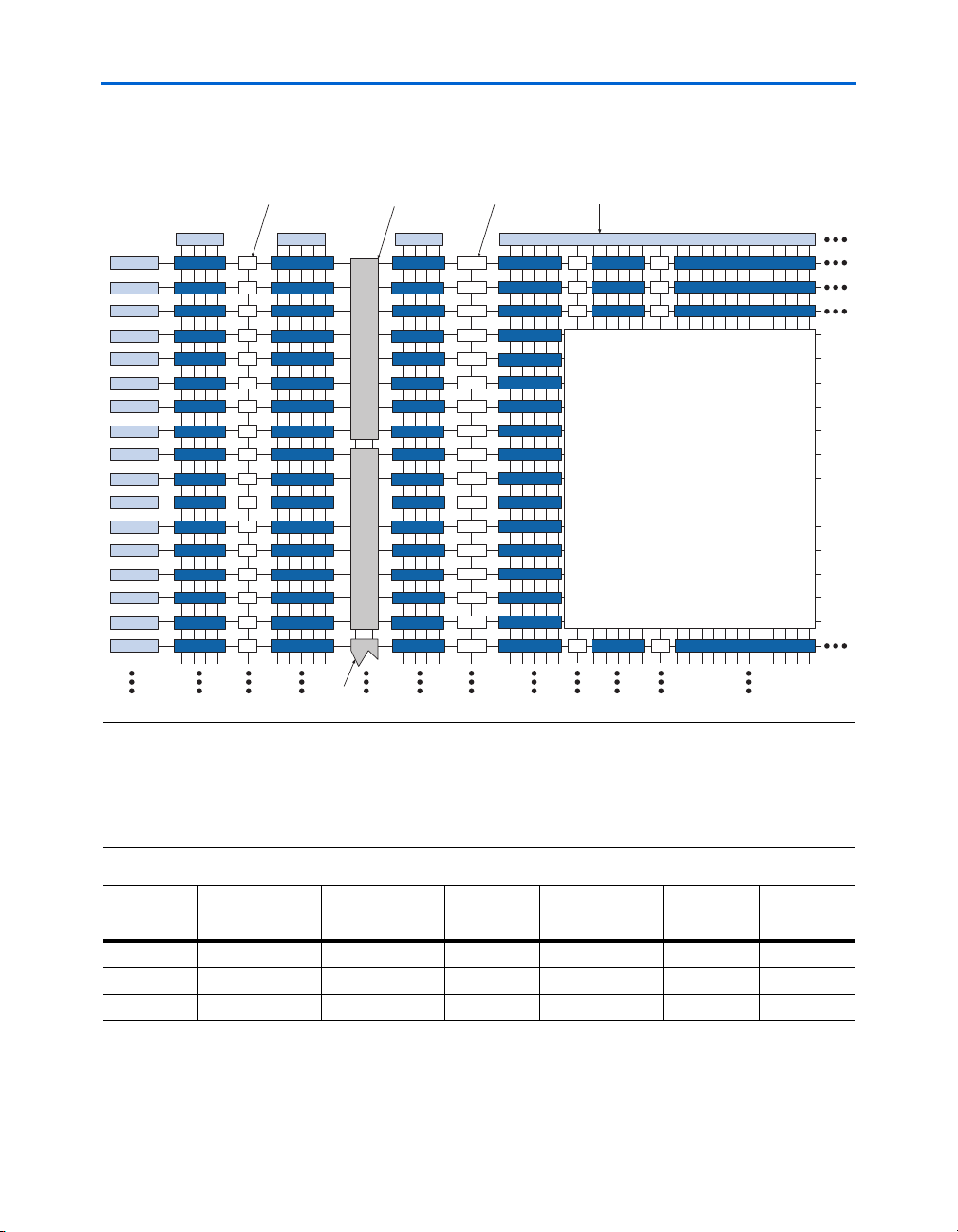
Figure 1–2. Stratix GX Block Diagram
M512 RAM Blocks for
Dual-Port Memory, Shift
Registers, & FIFO Buffers
DSP Blocks for
Multiplication and Full
Implementation of FIR Filters
Introduction to the Stratix GX Device Data Sheet
M4K RAM Blocks
for True Dual-Port
Memory & Other Embedded
Memory Functions
IOEs Support DDR, PCI, GTL+, SSTL-3,
SSTL-2, HSTL, LVDS, LVPECL, PCML,
HyperTransport & other I/O Standards
IOEs
IOEs
IOEs
IOEs
IOEs
IOEs
IOEs
IOEs
IOEs
IOEs
IOEs
IOEs
IOEs
IOEs
IOEs
IOEs
IOEs
IOEs
LABs
LABs
LABs
LABs
LABs
LABs
LABs
LABs
LABs
LABs
LABs
LABs
LABs
LABs
LABs
LABs
LABs
IOEs
LABs
LABs
LABs
LABs
LABs
LABs
LABs
LABs
LABs
LABs
LABs
LABs
LABs
LABs
LABs
LABs
LABs
DSP
Block
IOEs IOEs
LABs LABs
LABs
LABs LABs
LABs
LABs
LABs
LABs
LABs
LABs
LABs
LABs
LABs
LABs
LABs
LABs
LABs
LABs LABs
LABs
LABs
LABs
LABs
LABs
LABs
LABs
LABs
LABs
LABs
LABs
LABs
LABs
LABs
LABs
LABs
LABs
LABs
LABs
LABs
LABs
LABs
LABs
LABs
M-RAM Block
The number of M512 RAM, M4K RAM, and DSP blocks varies by device
along with row and column numbers and M-RAM blocks. Table 1–5 lists
the resources available in Stratix GX devices.
Table 1–5. Stratix GX Device Resources
Device
M512 RAM
Columns/Blocks
EP1SGX10 4 / 94 2 / 60 1 2 / 6 40 30
EP1SGX25 6 / 224 3 / 138 2 2 / 10 62 46
EP1SGX40 8 / 384 3 / 183 4 2 / 14 77 61
Altera Corporation 1–7
February 2005 Stratix GX Device Handbook, Volume 1
M4K RAM
Columns/Blocks
M-RAM
Blocks
DSP Block
Columns/Blocks
LAB
Columns
LAB Rows
Page 20

FPGA Functional Description
1–8 Altera Corporation
Stratix GX Device Handbook, Volume 1 February 2005
Page 21
SGX51002-1.1
2. Stratix GX Transceivers
Transceiver Blocks
Stratix®GX devices incorporate dedicated embedded circuitry on the
right side of the device, which contains up to 20 high-speed 3.1875-Gbps
serial transceiver channels. Each Stratix GX transceiver block contains
four full-duplex channels and supporting logic to transmit and receive
high-speed serial data streams. The transceiver block uses the channels to
deliver bidirectional point-to-point data transmissions with up to
3.1875 Gbps of data transition per channel.
There are up to 20 transceiver channels available on a single Stratix GX
device. Ta bl e 2 –1 shows the number of transceiver channels available on
each Stratix GX device.
Table 2–1. Stratix GX Transceiver Channels
Device Number of Transceiver Channels
EP1SGX10C 4
EP1SGX10D 8
EP1SGX25C 4
EP1SGX25D 8
EP1SGX25F 16
EP1SGX40D 8
EP1SGX40G 20
Figure 2–1 shows the elements of the transceiver block, including the four
channels, supporting logic, and I/O buffers. Each transceiver channel
consists of a receiver and transmitter. The supporting logic contains a
transmitter PLL to generate a high-speed clock used by the four
transmitters. The receiver PLL within each transceiver channel generates
the receiver reference clocks. The supporting logic also contains state
machines to manage rate matching for XAUI and GIGE applications, in
addition to channel bonding for XAUI applications.
Altera Corporation 2–1
June 2006
Page 22
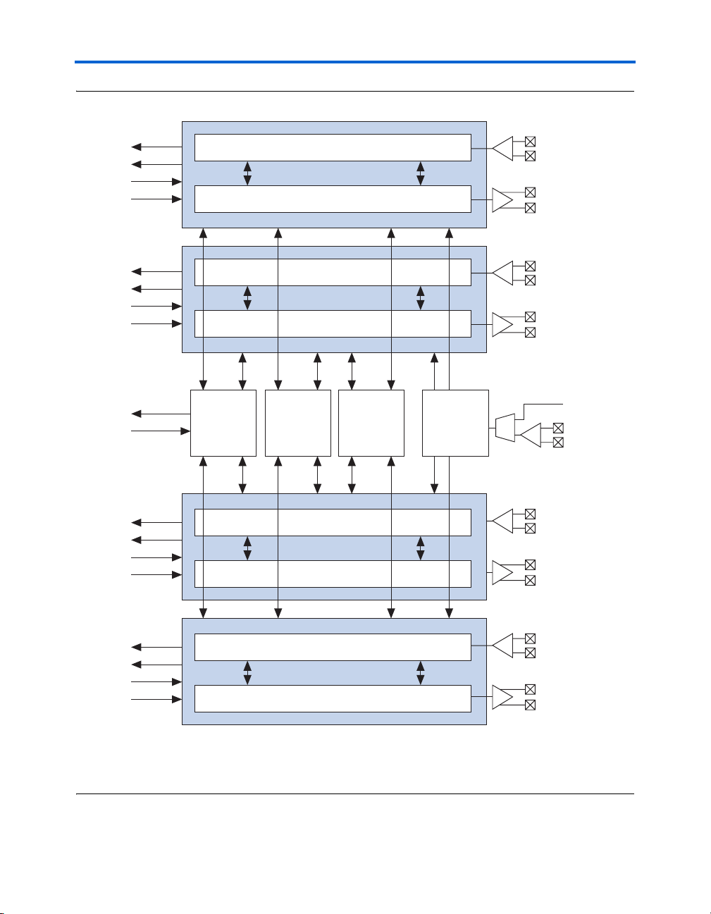
Figure 2–1. Stratix GX Transceiver Block Note (1)
PLD
Logic
Array
PLD
Logic
Array
PLD
Logic
Array
PLD
Logic
Array
XAUI
Receiver
State
Machine
Receiver Channel 0
Channel 0
Transmitter Channel 0
Receiver Channel 1
Channel 1
Transmitter Channel 1
XAUI
Transmitter
State
Machine
Receiver Channel 2
Channel 2
Transmitter Channel 2
Channel
Aligner
State
Machine
Transmitter
PLL
Receiver Pins
Transmitter Pins
Receiver Pins
Transmitter Pins
PLD
Logic
Array
(2)
Receiver Pins
Transmitter Pins
Receiver Pins
Transmitter Pins
PLD
Logic
Array
Receiver Channel 3
Channel 3
Transmitter Channel 3
Notes to Figure 2–1:
(1) Each receiver channel has its own PLL and CRU, which are not shown in this diagram. For more information, refer
to the section “Receiver Path” on page 2–13.
(2) For possible transmitter PLL clock inputs, refer to the section “Transmitter Path” on page 2–5.
2–2 Altera Corporation
Stratix GX Device Handbook, Volume 1 June 2006
Page 23

Stratix GX Transceivers
Each Stratix GX transceiver channel consists of a transmitter and receiver.
The transmitter contains the following:
■ Transmitter PLL
■ Transmitter phase compensation FIFO buffer
■ Byte serializer
■ 8B/10B encoder
■ Serializer (parallel to serial converter)
■ Transmitter output buffer
The receiver contains the following:
■ Input buffer
■ Clock recovery unit (CRU)
■ Deserializer
■ Pattern detector and word aligner
■ Rate matcher and channel aligner
■ 8B/10B decoder
■ Receiver logic array interface
You can set all the Stratix GX transceiver functions through the Quartus II
software. You can set programmable pre-emphasis, programmable
equalizer, and programmable V
dynamically as well. Each Stratix GX
OD
transceiver channel is also capable of BIST generation and verification in
addition to various loopback modes. Figure 2–2 shows the block diagram
for the Stratix GX transceiver channel.
Stratix GX transceivers provide physical coding sublayer (PCS) and
physical media attachment (PMA) implementation for protocols such as
10-gigabit XAUI and GIGE. The PCS portion of the transceiver consists of
the logic array interface, 8B/10B encoder/decoder, pattern detector, word
aligner, rate matcher, channel aligner, and the BIST and pseudo-random
binary sequence pattern generator/verifier. The PMA portion of the
transceiver consists of the serializer/deserializer, the CRU, and the I/O
buffers.
Altera Corporation 2–3
June 2006 Stratix GX Device Handbook, Volume 1
Page 24
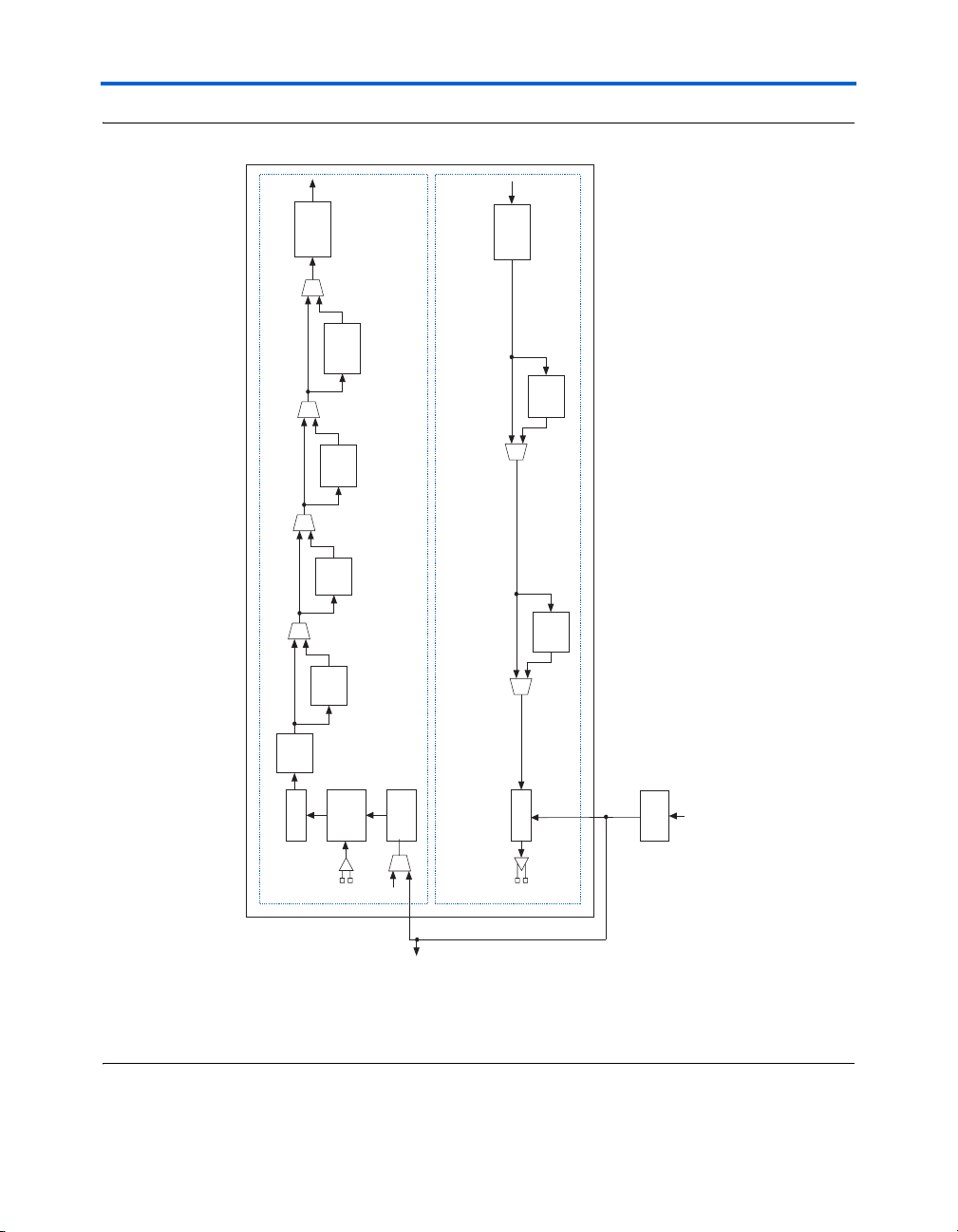
Figure 2–2. Stratix GX Transceiver ChanneL Note (1)
FIFO
Phase
Compensation
Byte
Deserializer
8B/10B
Decoder
Rate
Matcher
FIFO
Phase
Compensation
Byte
Serializer
8B/10B
Encoder
Aligner
Channel
Word
Aligner
Unit
Channel 0
Clock
Recovery
Deserializer
Receiver
PLL
Receiver
Transmitter
Clock
Receiver
Reference
To Channels 1-3
Serializer
PLL
Transmitter
Reference
Transmitter
Clock
Note to Figure 2–2:
(1) There are four transceiver channels in a transceiver block.
2–4 Altera Corporation
Stratix GX Device Handbook, Volume 1 June 2006
Page 25

Stratix GX Transceivers
Transmitter Path
This section describes the data path through the Stratix GX transmitter
(see Figure 2–2). Data travels through the Stratix GX transmitter via the
following modules:
■ Transmitter PLL
■ Transmitter phase compensation FIFO buffer
■ Byte serializer
■ 8B/10B encoder
■ Serializer (parallel to serial converter)
■ Transmitter output buffer
Transmitter PLL
Each transceiver block has one transmitter PLL, which receives the
reference clock and generates the following signals:
■ High-speed serial clock used by the serializer
■ Slow-speed reference clock used by the receiver
■ Slow-speed clock used by the logic array (divisible by two for
double-width mode)
The INCLK clock is the input into the transmitter PLL. There is one INCLK
clock per transceiver block. This clock can be fed by either the REFCLKB
pin, PLD routing, or the inter-transceiver routing line. See the section
“Stratix GX Clocking” on page 2–30 for more information about the inter-
transceiver lines.
The transmitter PLL in each transceiver block clocks the circuits in the
transmit path. The transmitter PLL is also used to train the receiver PLL.
If no transmit channels are used in the transceiver block, the transmitter
PLL can be turned off. Figure 2–3 is a block diagram of the transmitter
PLL.
Altera Corporation 2–5
June 2006 Stratix GX Device Handbook, Volume 1
Page 26
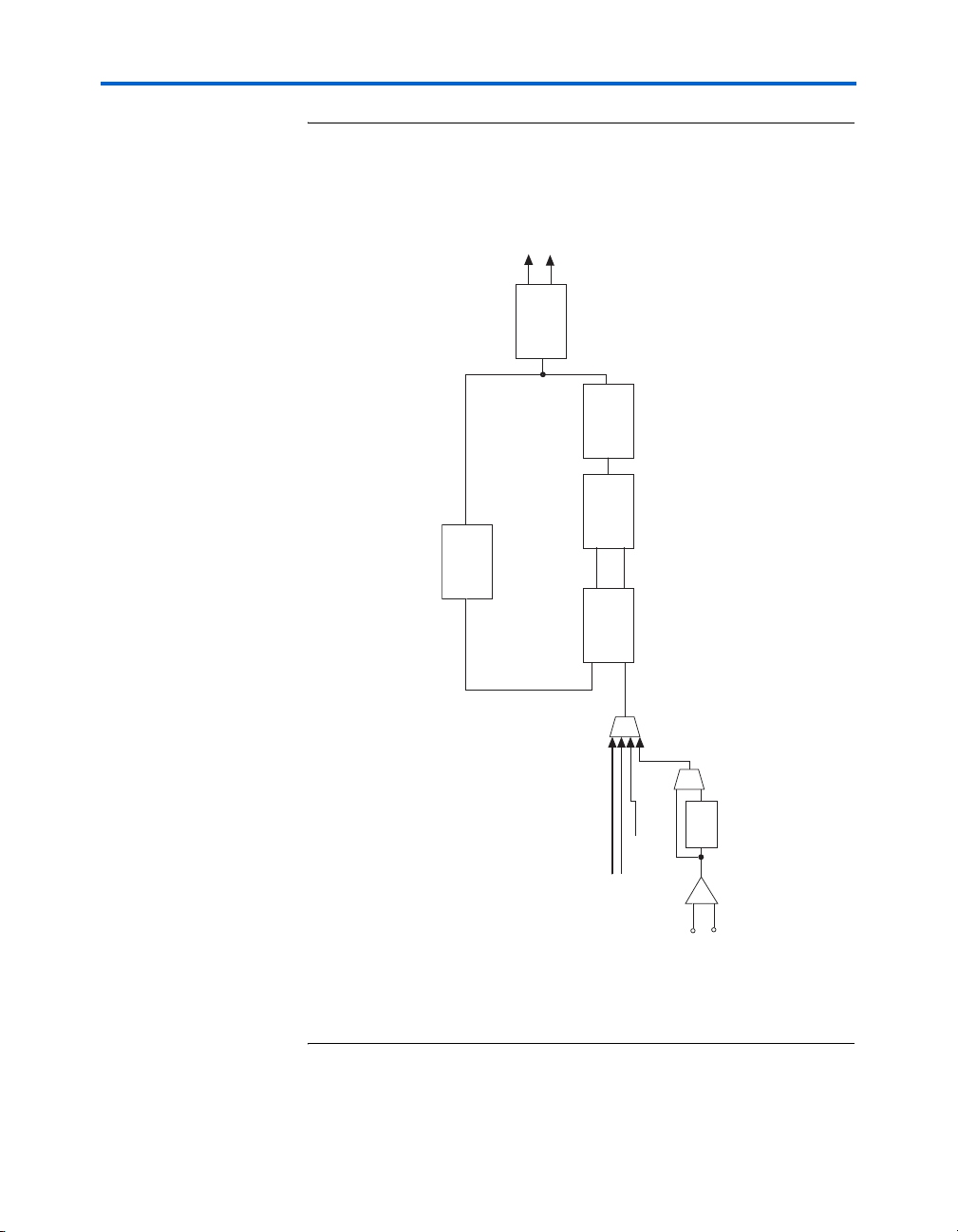
Figure 2–3. Transmitter PLL Block Diagram Note (1)
k
Low Speed Clock
High Speed Cloc
Clock
Driver
÷m
VCO
Charge Pump +
Loop Filter
Up
Down
PFD
INCLK
÷2
Inter Quad Routing (IQ1)
Inter Quad Routing (IQ0)
Global Clks, IO Bus, Gen Routing
Dedicated
Local
REFCLKB
Note to Figure 2–3:
(1) The divider in the PLL divides by 4, 8, 10, 16, or 20.
2–6 Altera Corporation
Stratix GX Device Handbook, Volume 1 June 2006
Page 27
Stratix GX Transceivers
The transmitter PLL can support up to 3.1875 Mbps. The input clock
frequency for –5 and –6 speed grade devices is limited to 650 MHz if you
use the REFCLKB pin or to 325 MHz if you use the other clock routing
resources. For –7 speed grade devices, the maximum input clock
frequency is 312.5 MHz with the REFCLKB pin, and the maximum is
156.25 MHz for all other clock routing resources. An optional
PLL_LOCKED port is available to indicate whether the transmitter PLL is
locked to the reference clock. The transmitter PLL has a programmable
loop bandwidth that can be set to low or high. The loop bandwidth
parameter can be statically set in the Quartus II software.
Table 2–2 lists the adjustable parameters in the transmitter PLL.
Table 2–2. Transmitter PLL Specifications
Parameter Specifications
Input reference frequency range 25 MHz to 650 MHz
Data rate support 500 Mbps to 3.1875 Gbps
Multiplication factor (W) 2, 4, 5, 8, 10, 16, or 20 (1)
Bandwidth Low, high
Note to Ta b l e 2 – 2:
(1) Multiplication factors 2 and 5 can only be achieved with the use of the pre-divider
on the REFCLKB pin.
Transmitter Phase Compensation FIFO Buffer
The transmitter phase compensation FIFO buffer resides in the
transceiver block at the PLD boundary. This FIFO buffer compensates for
the phase differences between the transmitter reference clock (inclk)
and the PLD interface clock (tx_coreclk). The phase difference
between the two clocks must be less than 360°. The PLD interface clock
must also be frequency locked to the transmitter reference clock. The
phase compensation FIFO buffer is four words deep and cannot be
bypassed.
Byte Serializer
The byte serializer takes double-width words (16 or 20 bits) from the PLD
interface and converts them to a single width word (8 or 10 bits) for use
in the transceiver. The transmit data path after the byte serializer is single
width (8 or 10 bits). The byte serializer is bypassed when single width
mode (8 or 10 bits) is used at the PLD interface.
Altera Corporation 2–7
June 2006 Stratix GX Device Handbook, Volume 1
Page 28
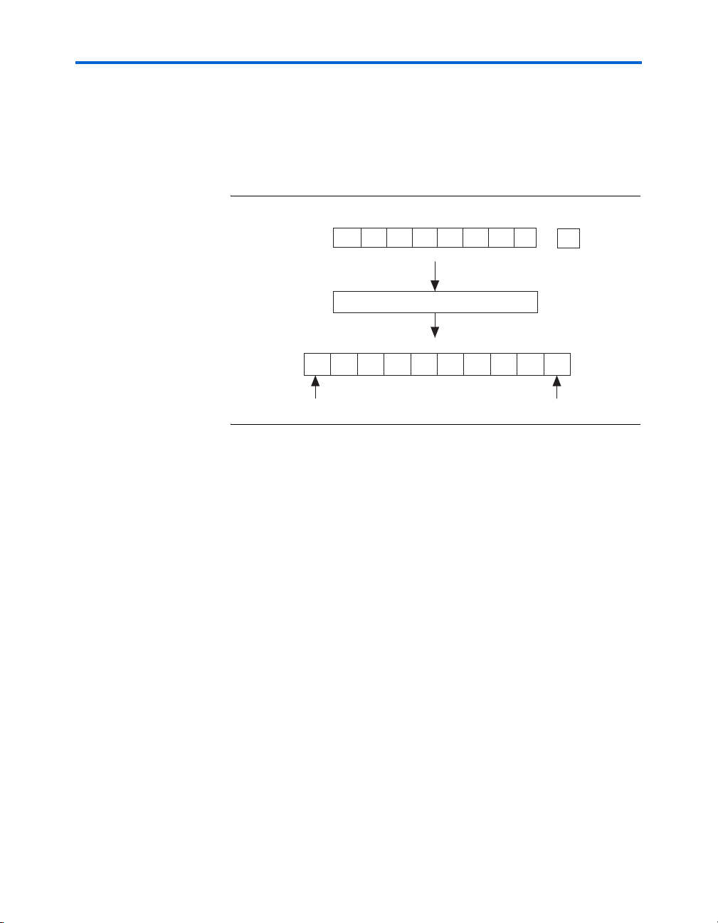
8B/10B Encoder
t
The 8B/10B encoder translates 8-bit wide data + 1 control enable bit into
a 10-bit encoded data. The encoded data has a maximum run length of 5.
The 8B/10B encoder can be bypassed. Figure 2–4 diagrams the encoding
process.
Figure 2–4. Encoding Process
+
76543210
HGFED CB A
8b-10b conversion
jhgfiedcba
9876543210
ctrl
MSB sent last
LSB sent firs
Transmit State Machine
The transmit state machine operates in either XAUI mode or in GIGE
mode, depending on the protocol used.
GIGE Mode
In GIGE mode, the transmit state machines convert all idle ordered sets
(/K28.5/, /Dx.y/) to either /I1/ or /I2/ ordered sets. /I1/ consists
of a negative-ending disparity /K28.5/ (denoted by /K28.5/-)
followed by a neutral /D5.6/. /I2/ consists of a positive-ending
disparity /K28.5/ (denoted by /K28.5/+) and a negative-ending
disparity /D16.2/ (denoted by /D16.2/-). The transmit state machines
do not convert any of the ordered sets to match /C1/ or /C2/, which are
the configuration ordered sets. (/C1/ and /C2/ are defined by
(/K28.5/, /D21.5/) and (/K28.5/, /D2.2/), respectively.) Both the
/I1/ and /I2/ ordered sets guarantee a negative-ending disparity after
each ordered set. The GIGE transmit state machine can be statically
disabled in the Quartus II software, even if using the GIGE protocol
mode.
2–8 Altera Corporation
Stratix GX Device Handbook, Volume 1 June 2006
Page 29
Stratix GX Transceivers
XAUI Mode
The transmit state machine translates the XAUI XGMII code group to the
XAUI PCS code group. Table 2–3 shows the code conversion.
Table 2–3. Code Conversion
XGMII TXC XGMII TXD PCS Code-Group Description
0 00 through FF Dxx.y Normal data
1 07 K28.0 or K28.3 or
K28.5
1 07 K28.5 Idle in ||T||
1 9C K28.4 Sequence
1 FB K27.7 Start
1 FD K29.7 Terminate
1 FE K30.7 Error
1 See IEEE 802.3
reserved code
groups
1 Other value K30.7 Invalid XGMII character
See IEEE 802.3
reserved code groups
Idle in ||I||
Reserved code groups
The XAUI PCS idle code groups, /K28.0/ (/R/) and /K28.5/ (/K/), are
7+x6
automatically randomized based on a PRBS7 pattern with an x
+1
polynomial. The /K28.3/ (/A/) code group is automatically generated
between 16 and 31 idle code groups. The idle randomization on the /A/,
/K/, and /R/ code groups are done automatically by the transmit state
machine.
Serializer (Parallel-to-Serial Converter)
The serializer converts the parallel 8-bit or 10-bit data into a serial stream,
transmitting the LSB first. The serialized stream is then fed to the transmit
buffer. Figure 2–5 is a diagram of the serializer.
Altera Corporation 2–9
June 2006 Stratix GX Device Handbook, Volume 1
Page 30
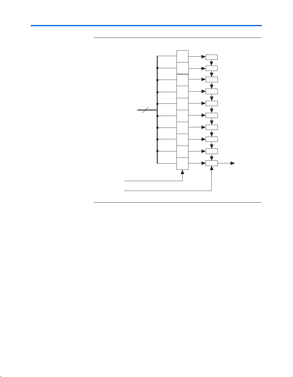
Figure 2–5. Serializer
Low-speed
parallel clock
High-speed
serial clock
Transmit Buffer
D9
D8
D7
D6
10
D5
D4
D3
D2
D1
D0
D9
D8
D7
D6
D5
D4
D3
D2
D1
D0
Serial data
out (to output
buffer)
The Stratix GX transceiver buffers support the 1.5-V pseudo current
mode logic (PCML) I/O standard at a rate up to 3.1875 Gbps, across up to
40 inches of FR4 trace, and across 2 connectors. Additional I/O standards,
LVDS, 3.3-V PCML, LVPECL, can be supported when AC coupled. The
common mode of the output driver is 750 mV.
The output buffer, as shown in Figure 2–6, consists of a programmable
output driver and a programmable pre-emphasis circuit.
2–10 Altera Corporation
Stratix GX Device Handbook, Volume 1 June 2006
Page 31

Figure 2–6. Output Buffer
Serializer
Output Buffer
Stratix GX Transceivers
Programmable
Termination
Output
Pins
Programmable
Output
Driver
Programmable
Pre-Emphasis
Programmable Output Driver
The programmable output driver can be set to drive out 400 to 1,600 mV.
Table 2–4 shows the available settings for each termination value. The
can be dynamically or statically set. The output driver requires either
V
OD
internal or external termination at the source.
Table 2–4. Programmable VOD (Differential) Note (1)
V
Termination Setting (Ω)
100 400, 800, 1000, 1200, 1400, 1600
120 480, 960, 1200, 1440
150 600, 1200, 1500
Note to Ta b l e 2 – 4:
(1) V
differential is measured as VA – VB (see Figure 2–7).
OD
Setting (mV)
OD
Altera Corporation 2–11
June 2006 Stratix GX Device Handbook, Volume 1
Page 32

Figure 2–7. VOD Differential
Single-Ended Waveform
Differential Waveform (VID (Differential) = 2 x VID (single-ended))
Positive Channel (p) = V
V
ID
V
CM
V
ID
Negative Channel (n) = V
Ground
p − n = 0 V
V
ID
OH
OL
Programmable Pre-Emphasis
The programmable pre-emphasis module controls the output driver to
boost the high frequency components, to compensate for losses in the
transmission medium, as shown in Figure 2–8. The pre-emphasis can be
dynamically or statically set. There are five possible pre-emphasis
settings (1 through 5), with 5 being the highest and 0 being no
pre-emphasis.
Figure 2–8. Programmable Pre-Emphasis Model
V
PP
V
S
V
CM
Bit
Time
Bit
Time
2–12 Altera Corporation
Stratix GX Device Handbook, Volume 1 June 2006
VPP(p-p)VS(p-p)
Page 33

Stratix GX Transceivers
Pre-emphasis percentage is defined as VPP/VS – 1, where VPP is the
differential emphasized voltage (peak-to-peak) and V
is the differential
S
steady-state voltage (peak-to-peak).
Programmable Transmitter Termination
The programmable termination can be statically set in the Quartus II
software. The values are 100 Ω, 120 Ω, 150 Ω, and off. Figure 2–9 shows the
setup for programmable termination.
Figure 2–9. Programmable Transmitter Termination
V
CM
Programmable
Output
Driver
50, 60, or 75
9
Receiver Path
This section describes the data path through the Stratix GX receiver (refer
to Figure 2–2 on page 2–4). Data travels through the Stratix GX receiver
via the following modules:
■ Input buffer
■ Clock Recovery Unit (CRU)
■ Deserializer
■ Pattern detector and word aligner
■ Rate matcher and channel aligner
■ 8B/10B decoder
■ Receiver logic array interface
Receiver Input Buffer
The Stratix GX receiver input buffer supports the 1.5-V PCML I/O
standard at a rate up to 3.1875 Gbps. Additional I/O standards, LVDS,
3.3-V PCML, and LVPECL can be supported when AC coupled. The
common mode of the input buffer is 1.1 V. The receiver can support
Stratix GX-to-Stratix GX DC coupling.
Altera Corporation 2–13
June 2006 Stratix GX Device Handbook, Volume 1
Page 34

Figure 2–10 shows a diagram of the receiver input buffer, which contains:
■ Programmable termination
■ Programmable equalizer
Figure 2–10. Receiver Input Buffer
Programmable
Termination
Input
Pins
Programmable
Equalizer
Differential
Input
Buffer
Programmable Termination
The programmable termination can be statically set in the Quartus II
software. Figure 2–11 shows the setup for programmable receiver
termination.
Figure 2–11. Programmable Receiver Termination
Differential
50, 60, or 75 Ω
50, 60, or 75 Ω
V
CM
Input
Buffer
If you use external termination, then the receiver must be externally
terminated and biased to 1.1 V. Figure 2–12 shows an example of an
external termination/biasing circuit.
2–14 Altera Corporation
Stratix GX Device Handbook, Volume 1 June 2006
Page 35

Figure 2–12. External Termination & Biasing Circuit
Stratix GX Transceivers
50/60/75Termination
Resistance
Transmission
Receiver External Termination
and Biasing
Ω
R1/R2 = 1K
V
× {R2/(R1 + R 2)} = 1.1 V
DD
Receiver External Termination
Line
V
DD
C1
and Biasing
R1
R2
Stratix GX Device
Receiver
RXIP
RXIN
Programmable Equalizer
The programmable equalizer module boosts the high frequency
components of the incoming signal to compensate for losses in the
transmission medium. There are five possible equalization settings (0, 1,
2, 3, 4) to compensate for 0”, 10”, 20”, 30”, and 40” of FR4 trace. These
settings should be interpreted loosely. The programmable equalizer can
be set dynamically or statically.
Receiver PLL & CRU
Each transceiver block has four receiver PLLs and CRUs, each of which is
dedicated to a receive channel. If the receive channel associated with a
particular receiver PLL or CRU is not used, then the receiver PLL or CRU
is powered down for the channel. Figure 2–13 is a diagram of the receiver
PLL and CRU circuits.
Altera Corporation 2–15
June 2006 Stratix GX Device Handbook, Volume 1
Page 36

Figure 2–13. Receiver PLL & CRU Circuit
Receiver PLL
÷ m (1)
rx_locked
Low-Speed TX_PLL_CLK
Inter Transceiver Routing (IQ2)
Global Clks, IO Bus, Gen Routing
Dedicated
Local
REFCLKB
Note to Figure 2–13:
(1) m = 8, 10 16, or 20.
PFD
up
÷ 2
rx_locktorefclk
rx_locktodata
RX_IN
RX CRUCLK
down
down
up
CRU
Charge Pump
and Loop Filter
VCO
rx_freqlocked[]
rx_riv[ ]
High-speed RCVD_CLK
Low-speed RCVD_CLK
The receiver PLLs and CRUs are capable of supporting up to 3.1875 Gbps.
The input clock frequency for –5 and –6 speed grade devices is limited to
650 MHz if you use the REFCLKB pin or 325 MHz if you use the other
clock routing resources. The maximum input clock frequency for –7 speed
grade devices is 312.5 MHz if you use the REFCLKB pin or 156.25 MHz
with the other clock routing resources. An optional RX_LOCKED port
(active low signal) is available to indicate whether the PLL is locked to the
reference clock. The receiver PLL has a programmable loop bandwidth,
which can be set to low, medium, or high. The loop bandwidth parameter
can be statically set by the Quartus II software.
Table 2–5 lists the adjustable parameters of the receiver PLL and CRU. All
the parameters listed are statically programmable in the Quartus II
software.
Table 2–5. Receiver PLL & CRU Adjustable Parameters (Part 1 of 2)
Parameter Specifications
Input reference frequency range 25 MHz to 650 MHz
Data rate support 500 Mbps to 3.1875 Gbps
2–16 Altera Corporation
Stratix GX Device Handbook, Volume 1 June 2006
Page 37

Stratix GX Transceivers
Table 2–5. Receiver PLL & CRU Adjustable Parameters (Part 2 of 2)
Multiplication factor (W) 2, 4, 5, 8, 10, 16, or 20 (1)
PPM detector 125, 250, 500, 1,000
Bandwidth Low, medium, high
Run length detector 10-bit or 20-bit mode: 5 to 160 in steps of
5
8-bit or 16-bit mode: 4 to 128 in steps of 4
Note to Ta b l e 2 – 5:
(1) Multiplication factors 2, 4, and 5 can only be achieved with the use of the pre-
divider on the REFCLKB port or if the CRU is trained with the low speed clock
from the transmitter PLL.
The CRU has a built-in switchover circuit to select whether the
voltage-controlled oscillator of the PLL is trained by the reference clock or
the data. The optional port rx_freqlocked monitors when the CRU is
in locked to data mode.
In the automatic mode, the following conditions must be met for the CRU
to switch from locked to reference to locked to data mode:
■ The CRU PLL is within the prescribed PPM frequency threshold
setting (125 PPM, 250 PPM, 500 PPM, 1,000 PPM) of the CRU
reference clock.
■ The reference clock and CRU PLL output are phase matched (phases
are within .08 UI).
The automatic switchover circuit can be overridden by using the optional
ports rx_lockedtorefclk and rx_locktodata. Table 2–6 shows the
possible combinations of these two signals.
Table 2–6. Possible Combinations of rx_lockedtorefclk & rx_locktodata
rx_locktodata rx_lockedtorefclk VCO (lock to mode)
00Auto
0 1 Reference CLK
1xDATA
If the rx_lockedtorefclk and rx_locktodata ports are not used,
the default is auto mode.
Altera Corporation 2–17
June 2006 Stratix GX Device Handbook, Volume 1
Page 38

Deserializer (Serial-to-Parallel Converter)
The deserializer converts the serial stream into a parallel 8- or 10-bit data
bus. The deserializer receives the least significant bit first. Figure 2–14 is
a diagram of the deserializer.
Figure 2–14. Deserializer
High-speed
serial clock
Low-speed
parallel clock
Word Aligner
D9
D8
D7
D6
D5
D4
D3
D2
D1
D0
D7
D6
D5
D4
D3
D2
D1
D0
D9
D8
10
The word aligner aligns the incoming data based on the specific byte
boundaries. The word aligner has three customizable modes of operation:
bit-slip mode, 16-bit mode, and 10-bit mode, the last of which is available
for the basic and SONET modes. The word aligner also has two
non-customizable modes of operation, which are the XAUI and GIGE
modes.
Figure 2–15 shows the word aligner in bit-slip mode.
2–18 Altera Corporation
Stratix GX Device Handbook, Volume 1 June 2006
Page 39

Figure 2–15. Word Aligner in Bit-Slip Mode
Stratix GX Transceivers
Word Aligner
Bit-Slip
Mode
Manual
Alignment
Mode
10-Bit
Mode
Patterm Detector
A1A2
Mode
16-Bit
Mode
A1A1A2A2
Mode
7-Bit
Mode
In the bit-slip mode, the byte boundary can be modified by a barrel shifter
to slip the byte boundary one bit at a time via a user-controlled bit-slip
port. The bit-slip mode supports both 8-bit and 10-bit data paths
operating in a single or double-width mode.
The pattern detector is active in the bit-slip mode, and it detects the
®
user-defined pattern that is specified in the MegaWizard
Plug-In
Manager.
The bit-slip mode is available only in Custom mode and SONET mode.
Figure 2–16 shows the word aligner in 16-bit mode.
Altera Corporation 2–19
June 2006 Stratix GX Device Handbook, Volume 1
Page 40

Figure 2–16. Word Aligner in 16-Bit Mode
Word Aligner
A1A2
Mode
Manual
Alignment
Mode
16-Bit
Mode
A1A1A2A2
Mode
A1A2
Mode
Pattern Detector
16-Bit
Mode
A1A1A2A2
Mode
In the 16-bit mode, the word aligner and pattern detector automatically
aligns and detects a user-defined 16-bit alignment pattern. This pattern
can be in the format of A1A2 or A1A1A2A2 (for the SONET protocol). The
re-alignment of the byte boundary can be done via a user-controlled port.
The 16-bit mode supports only the 8-bit data path in a single-width or
double-width mode.
The 16-bit mode is available only for the Custom mode and SONET
mode. The A1A1A2A2 word alignment pattern option is available only
for the SONET mode and cannot be used in the Custom mode.
Figure 2–17 shows the word aligner in 10-bit mode.
2–20 Altera Corporation
Stratix GX Device Handbook, Volume 1 June 2006
Page 41

Figure 2–17. Word Aligner in 10-Bit Mode
Stratix GX Transceivers
Word Aligner
Manual
Alignment
Mode
10-Bit
Mode
10-Bit
Mode
Pattern Detector
7-Bit
Mode
In the 10-bit mode, the word aligner automatically aligns the user’s
predefined 10-bit alignment pattern. The pattern detector can detect the
full 10-bit pattern or only the lower seven bits of the pattern. The word
aligner and pattern detector detect both the positive and the negative
disparity of the pattern. A user-controlled enable port is available for the
word aligner.
The 10-bit mode is available only for the Custom mode.
Figure 2–18 shows the word aligner in XAUI mode.
Altera Corporation 2–21
June 2006 Stratix GX Device Handbook, Volume 1
Page 42

Figure 2–18. Word Aligner in XAUI Mode
Word Aligner
Synchronization
State Machines
GigE
Mode
XAUI
Mode
In the XAUI and GIGE modes, the word alignment is controlled by a state
machine that adheres to the IEEE 802.3ae standard for XAUI and the
IEEE 802.3 standard for GIGE. The alignment pattern is predefined to be
a /K28.5/ code group.
The XAUI mode is available only for the XAUI protocol, and the GIGE
mode is available only for the GIGE protocol.
Channel Aligner
The channel aligner is available only in XAUI mode and bonds all four
channels within a transceiver. The channel aligner adheres to the
IEEE 802.3ae, clause 48 specification for channel bonding.
The channel aligner is a 16-word deep FIFO buffer with a state machine
overlooking the channel bonding process. The state machine looks for an
/A/ (/K28.3/) in each channel and aligns all the /A/s in the transceiver.
When four columns of /A/ (denoted by //A//) are detected, the
rx_channelalign port goes high, signifying that all the channels in the
transceiver have been bonded. The reception of four consecutive
misaligned /A/s restarts the channel alignment sequence and de-asserts
rx_channelalign.
Figure 2–19 shows misaligned channels before the channel aligner and
the channel alignment after the channel aligner.
2–22 Altera Corporation
Stratix GX Device Handbook, Volume 1 June 2006
Page 43

Figure 2–19. Before & After the Channel Aligner
Stratix GX Transceivers
Lane 0
Lane 0
Lane 0
Lane 0
Lane 0
Lane 0
KRKKKRRRKKRA
Lane 0
Lane 0
KRKKKRRRKKRA
KRKKKRRRKKRA
KRKKKRRRKKRA
KRKKKRRRKKRA
KRKKKRRRKKRA
KRKKKRRRKKRA
KRKKKRRRKKRA
Rate Matcher
The rate matcher, which is available only in XAUI and GIGE modes,
consists of a 12-word deep FIFO buffer and a FIFO controller. The rate
matcher is bypassed when the device is not in XAUI or GIGE mode.
In a multi-crystal environment, the rate matcher compensates for up to a
100-ppm difference between the source and receiver clocks.
GIGE Mode
In the GIGE mode, the rate matcher adheres to the specifications in
clause 36 of the IEEE 802.3 documentation, for idle additions or removals.
The rate matcher performs clock compensation only on /I2/ ordered
sets, composing a /K28.5/+ followed by a /D16.2/-. The rate matcher
does not perform a clock compensation on any other ordered set
combinations. An /I2/ is added or deleted automatically based on the
number of words in the FIFO buffer. A 9’h19C is given at the control and
data ports when the FIFO is in an overflow or underflow condition.
Altera Corporation 2–23
June 2006 Stratix GX Device Handbook, Volume 1
Page 44

XAUI Mode
In XAUI mode, the rate matcher adheres to clause 48 of the IEEE 802.3ae
specification for clock rate compensation. The rate matcher performs
clock compensation on columns of /R/ (/K28.0/), denoted by //R//.
An //R// is added or deleted automatically based on the number of
words in the FIFO buffer.
8B/10B Decoder
The 8B/10B decoder converts the 10-bit encoded code group into 8-bit
data and 1 control bit. The 8B/10B decoder can be bypassed. The
following is a diagram of the conversion from a 10-bit encoded code
group into 8-bit data + 1-bit control.
Figure 2–20. 8B/10B Decoder Conversion
jhgfiedcba
9876543210
MSB received last
Parallel data
8b-10b conversion
76543210
HGFED CB A
LSB received first
+
ctrl
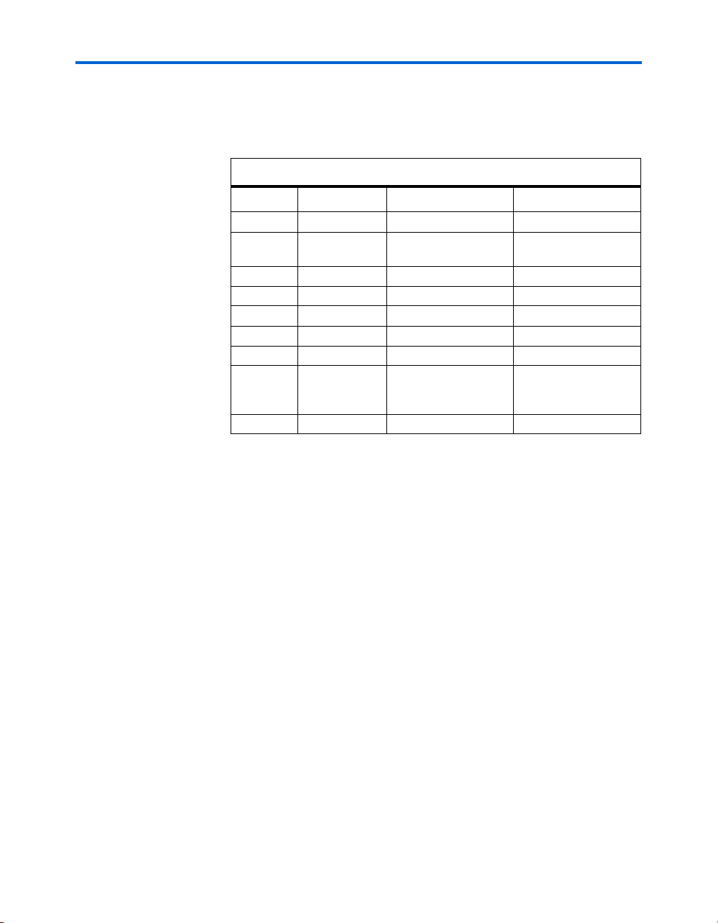
There are two optional error status ports available in the 8B/10B decoder,
rx_errdetect and rx_disperr. Table 2–7 shows the values of the
ports from a given error. These status signals are aligned with the code
group in which the error occurred.
Table 2–7. Error Signal Values
Types of Errors rx_errdetect rx_disperr
No errors 1’b0 1’b0
Invalid code groups 1’b1 1’b0
Disparity errors 1’b1 1’b1
2–24 Altera Corporation
Stratix GX Device Handbook, Volume 1 June 2006
Page 45

Stratix GX Transceivers
Receiver State Machine
The receiver state machine operates in GIGE and XAUI modes. In GIGE
mode, the receiver state machine replaces invalid code groups with
9’h1FE. In XAUI mode, the receiver state machine translates the XAUI
PCS code group to the XAUI XGMII code group. Table 2–8 shows the
code conversion. The conversion adheres to the IEEE 802.3ae
specification.
Table 2–8. Code Conversion
XGMII RXC XGMII RXD PCS code-group Description
0 00 through FF Dxx.y Normal Data
1 07 K28.0 or K28.3 or K28.5 Idle in ||I||
1 07 K28.5 Idle in ||T||
1 9C K28.4 Sequence
1 FB K27.7 Start
1 FD K29.7 Terminate
1FE K30.7 Error
1 FE Invalid code group Invalid XGMII character
1 See IEEE 802.3 reserved code
groups
See IEEE 802.3 reserved
code groups
Reserved code groups
Byte Deserializer
The byte deserializer takes a single width word (8 or 10 bits) from the
transceiver logic and converts it into double-width words (16 or 20 bits)
to the phase compensation FIFO buffer. The byte deserializer is bypassed
when single width mode (8 or 10 bits) is used at the PLD interface.
Phase Compensation FIFO Buffer
The receiver phase compensation FIFO buffer resides in the transceiver
block at the programmable logic device (PLD) boundary. This buffer
compensates for the phase difference between the recovered clock within
the transceiver and the recovered clock after it has transferred to the PLD
core. The phase compensation FIFO buffer is four words deep and cannot
be bypassed.
Altera Corporation 2–25
June 2006 Stratix GX Device Handbook, Volume 1
Page 46

Loopback Modes
The Stratix GX transceiver has built-in loopback modes to aid in debug
and testing. The loopback modes are set in the Stratix GX MegaWizard
Plug-In Manager in the Quartus II software. Only one loopback mode can
be set at any single instance of the transceiver block. The loopback mode
applies to all used channels in a transceiver block.
The available loopback modes are:
■ Serial loopback
■ Parallel loopback
■ Reverse serial loopback
Serial Loopback
Serial loopback exercises all the transceiver logic except for the output
buffer and input buffer. The loopback function is dynamically switchable
through the rx_slpbk port on a channel by channel basis. The VOD of the
output reduced. If you select 400 mV, the output is tri-stated when the
serial loopback option is selected. Figure 2–21 shows the data path in
serial loopback mode.
Figure 2–21. Data Path in Serial Loopback Mode
BIST PRBS
Verifier
Clock
Unit
Word
Aligner
Channel
Aligner
Rate
Matcher
Deserializer
Recovery
8B/10B
Decoder
Byte
Deserializer
BIST
Incremental
Verifier
Phase
Compensation
FIFO
Serializer
Active Path
Non-Active Path
8B/10B
Encoder
BIST PRBS
Generator
Byte
Serializer
Phase
Compensation
FIFO
BIST
Generator
2–26 Altera Corporation
Stratix GX Device Handbook, Volume 1 June 2006
Page 47

Parallel Loopback
The parallel loopback mode exercises the digital logic portion of the
transceiver data path. The analog portions are not use in the loopback
path. The received data is not retimed. Figure 2–22 shows the data path in
parallel loopback mode. This option is not dynamically switchable.
Reception of an external signal is not possible in this mode.
Figure 2–22. Data Path in Parallel Loopback Mode
BIST PRBS
Verifier
Deserializer
Clock
Recovery
Unit
Word
Aligner
Channel
Aligner
Rate
Matcher
8B/10B
Decoder
Stratix GX Transceivers
Byte
Deserializer
BIST
Incremental
Verifier
Phase
Compensation
FIFO
Serializer
Active Path
Non-Active Path
8B/10B
Encoder
BIST PRBS
Generator
Byte
Serializer
Phase
Compensation
FIFO
BIST
Generator
Reverse Serial Loopback
The reverse serial loopback exercises the analog portion of the
transceiver. This loopback mode is dynamically switchable through the
tx_srlpbk port on a channel by channel basis. Asserting
rxanalogreset in reverse serial loopback mode powers down the
receiver buffer and CRU, preventing data loopback. Figure 2–23 shows
the data path in reverse serial loopback mode.
Altera Corporation 2–27
June 2006 Stratix GX Device Handbook, Volume 1
Page 48

Figure 2–23. Data Path in Reverse Serial Loopback Mode
BIST PRBS
Verifier
Unit
Word
Aligner
Channel
Aligner
Rate
Matcher
Deserializer
Clock
Recovery
8B/10B
Decoder
Byte
Deserializer
BIST
Incremental
Verifier
Phase
Compensation
FIFO
Active Path
Non-Active Path
Serializer
8B/10B
Encoder
BIST PRBS
Generator
Byte
Serializer
Phase
Compensation
FIFO
BIST
Generator
BIST (Built-In Self Test)
The Stratix GX transceiver has built-in self test modes to aid in debug and
testing. The BIST modes are set in the Stratix GX MegaWizard Plug-In
Manager in the Quartus II software. Only one BIST mode can be set for
any single instance of the transceiver block. The BIST mode applies to all
channels used in a transceiver.
The following is a list of the available BIST modes:
■ PRBS generator and verifier
■ Incremental mode generator and verifier
■ High-frequency generator
■ Low-frequency generator
■ Mixed-frequency generator
Figures 2–24 and 2–25 are diagrams of the BIST PRBS data path and the
BIST incremental data path, respectively.
2–28 Altera Corporation
Stratix GX Device Handbook, Volume 1 June 2006
Page 49

Figure 2–24. BIST PRBS Data Path
Deserializer
Recovery
Clock
Unit
Word
Aligner
Channel
BIST PRBS
Verifier
Aligner
Rate
Matcher
8B/10B
Decoder
Stratix GX Transceivers
Byte
Deserializer
BIST
Incremental
Verifier
Phase
Compensation
FIFO
Serializer
Active Path
BIST PRBS
Non-active Path
Figure 2–25. BIST Incremental Data Path
BIST PRBS
Verifier
Deserializer
Recovery
Active Path
Clock
Unit
Serializer
Word
Aligner
Channel
Aligner
BIST PRBS
Non-active Path
Table 2–9 shows the BIST data output and verifier alignment pattern.
8B/10B
Encoder
Generator
8B/10B
Encoder
Generator
Rate
Matcher
Byte
Serializer
8B/10B
Decoder
Byte
Serializer
Phase
Compensation
FIFO
Byte
Deserializer
Phase
Compensation
FIFO
BIST
Incremental
Verifier
Phase
Compensation
FIFO
BIST
Generator
BIST
Generator
Table 2–9. BIST Data Output & Verifier Alignment Pattern (Part 1 of 2)
BIST Mode Output Polynomials Verifier Word Alignment Pattern
PRBS 8-bit
PRBS 10-bit
Altera Corporation 2–29
June 2006 Stratix GX Device Handbook, Volume 1
8
2
– 1 x8 + x7 + x5 + x3 + 1
10
– 1 x10 + x7 + 1
2
1000000011111111
1111111111
Page 50

Table 2–9. BIST Data Output & Verifier Alignment Pattern (Part 2 of 2)
BIST Mode Output Polynomials Verifier Word Alignment Pattern
PRBS 16-bit
PRBS 20-bit
Incremental 10-bit K28.5, K27.7, Data (00-FF
Incremental 20-bit K28.5, K27.7, Data (00-FF
High frequency 1010101010
Low frequency 0011111000
Mixed frequency 0011111010 or 1100000101
Note to Ta b le 2 –9 :
(1) This output repeats.
8
– 1 x8 + x7 + x5 + x3 + 1
2
10
2
– 1 x10 + x7 + 1
incremental), K28.0, K28.1,
K28.2, K28.3, K28.4, K28.6,
K28.7, K23.7, K30.7, K29.7 (1)
incremental), K28.0, K28.1,
K28.2, K28.3, K28.4, K28.6,
K28.7, K23.7, K30.7, K29.7 (1)
1000000011111111
1111111111
0101111100 (K28.5)
0101111100 (K28.5)
Stratix GX Clocking
The Stratix GX global clock can be driven by certain REFCLKB pins, all
transmitter PLL outputs, and all receiver PLL outputs. The REFCLKB pins
(except for transceiver block 0 and transceiver block 4) can drive intertransceiver and global clock lines as well as feed the transmitter and
receiver PLLs. The output of the transmitter PLL can only feed global
clock lines and the reference clock port of the receiver PLL.
Figures 2–26 and 2–27 are diagrams of the Inter-Transceiver line
connections as well as the global clock connections for the EP1SGX25F
and EP1SGX40G devices. For devices with fewer transceivers, ignore the
information about the unavailable transceiver blocks.
2–30 Altera Corporation
Stratix GX Device Handbook, Volume 1 June 2006
Page 51

Stratix GX Transceivers
s
Figure 2–26. EP1SGX25F Device Inter-Transceiver & Global Clock Connections Note (1)
Transceiver Block 0
IQ0
IQ0 IQ1 IQ2
Global Clocks, I/O Bus, General Routing
Global Clocks, I/O Bus, General Routing
Global Clocks, I/O Bus, General Routing
Global Clocks, I/O Bus, General Routing
IQ1
refclkb
IQ2
Transceiver Block 1
IQ0
IQ1
refclkb
IQ2
/2
/2
Transmitter
PLL
Transmitter
PLL
4
Receiver
PLLs
4
Receiver
PLLs
4
(2)
4
Transceiver Block 2
IQ0
Global Clocks, I/O Bus, General Routing
Global Clocks, I/O Bus, General Routing
Global Clocks, I/O Bus, General Routing
Global Clocks, I/O Bus, General Routing
IQ1
refclkb
IQ2
Transceiver Block 3
IQ0
IQ1
refclkb
IQ2
/2
/2
Transmitter
PLL
Transmitter
PLL
4
Receiver
PLLs
4
Receiver
PLLs
(2)
4
(2)
4
16
PLD Global Clock
Notes to Figure 2–26:
(1) IQ lines are inter-transceiver block lines.
(2) If the /2 pre-divider is used, the path to drive the PLD logic array, local, or global clocks is not allowed.
(3) There are four receiver PLLs in each transceiver block.
Altera Corporation 2–31
June 2006 Stratix GX Device Handbook, Volume 1
Page 52

Figure 2–27. EP1SGX40G Device Inter-Transceiver & Global Clock Connections Note (1)
Transceiver Block 0
IQ0
Global Clks, I/O Bus, Gen Routing
refclkb
Global Clks, I/O Bus, Gen Routing
IQ1
TX PLL
/2
IQ2
4
Receiver
PLLs
4
IQ0 IQ1 IQ2
Transceiver Block 1
Global Clks, I/O Bus, Gen Routing
refclkb
Global Clks, I/O Bus, Gen Routing
IQ0
IQ1
/2
IQ2
Transceiver Block 4
IQ0
Global Clks, I/O Bus, Gen Routing
refclkb
Global Clks, I/O Bus, Gen Routing
Transceiver Block 2
Global Clks, I/O Bus, Gen Routing
refclkb
Global Clks, I/O Bus, Gen Routing
Transceiver Block 3
Global Clks, I/O Bus, Gen Routing
refclkb
Global Clks, I/O Bus, Gen Routing
IQ1
/2
IQ2
IQ0
IQ1
/2
IQ2
IQ0
IQ1
/2
IQ2
TX PLL
TX PLL
TX PLL
TX PLL
4
Receiver
PLLs
4
Receiver
PLLs
4
Receiver
PLLs
4
Receiver
PLLS
(2)
4
PLD
Global
Clocks
16
4
(2)
4
(2)
4
Notes to Figure 2–27:
(1) IQ lines are inter-transceiver block lines.
(2) If the /2 pre-divider is used, the path to drive the PLD logic array, local, or global clocks is not allowed.
(3) There are four receiver PLLs in each transceiver block.
2–32 Altera Corporation
Stratix GX Device Handbook, Volume 1 June 2006
Page 53

Stratix GX Transceivers
The receiver PLL can also drive the fast regional, regional clocks, and
local routing adjacent to the associated transceiver block. Figures 2–28
through 2–31 show which fast regional and regional clock resource can be
used by the recovered clock.
In the EP1SGX25 device, the receiver PLL recovered clocks from
transceiver blocks 0 and 1 drive RCLK[1..0] while transceiver blocks 2
and 3 drive RCLK[7..6]. The regional clocks feed logic in their
associated regions.
Figure 2–28. EP1SGX25 Receiver PLL Recovered Clock to Regional Clock
Connection
PLD
RCLK[11..10]
Stratix GX
Transceiver Blocks
Block 0
Block 1
Block 2
RCLK[9..8]
Block 3
In addition, the receiver PLL’s recovered clocks can drive fast regional
lines (FCLK) as shown Figure 2–29. The fast regional clocks can feed logic
in their associated regions.
Altera Corporation 2–33
June 2006 Stratix GX Device Handbook, Volume 1
Page 54

Figure 2–29. EP1SGX25 Receiver PLL Recovered Clock to Fast Regional Clock
Connection
Stratix GX
PLD
FCLK[1..0]
FCLK[1..0]
Transceiver Blocks
Block 0
Block 1
Block 2
Block 3
In the EP1SGX40 device, the receiver PLL recovered clocks from
transceivers 0 and 1 drive RCLK[1..0] while transceivers 2, 3, and 4
drive RCLK[7..6]. The regional clocks feed logic in their associated
regions.
2–34 Altera Corporation
Stratix GX Device Handbook, Volume 1 June 2006
Page 55

Stratix GX Transceivers
Figure 2–30. EP1SGX40 Receiver PLL Recovered Clock to Regional Clock
Connection
PLD
RCLK[11..10]
RCLK[9..8]
Stratix GX
Transceiver Blocks
Block 0
Block 1
Block 4
Block 2
Block 3
Figure 2–31 shows the possible recovered clock connection to the fast
regional clock resource. The fast regional clocks can drive logic in their
associated regions.
Altera Corporation 2–35
June 2006 Stratix GX Device Handbook, Volume 1
Page 56

Figure 2–31. EP1SGX40 Receiver PLL Recovered Clock to Fast Regional Clock
Connection
Stratix GX
PLD
FCLK[1..0]
FCLK[1..0]
Transceiver Blocks
Block 0
Block 1
Block 4
Block 2
Block 3
Table 2–10 summarizes the possible clocking connections for the
transceivers.
Table 2–10. Possible Clocking Connections for Transceivers (Part 1 of 2)
Destination
Source
REFCLKB vvv (1) vv (1)
Transmitter PLL vvvv
Receiver PLL vvv
GCLK vv
RCLK vv
FCLK vv
2–36 Altera Corporation
Stratix GX Device Handbook, Volume 1 June 2006
Transmitter
PLL
Receiver
PLL
GCLK RCLK FCLK IQ Lines
Page 57

Stratix GX Transceivers
Table 2–10. Possible Clocking Connections for Transceivers (Part 2 of 2)
Destination
Source
IQ lines v (2) v (2)
Notes to Table 2–10:
(1) REFCLKB from transceiver block 0 and transceiver block 4 does not drive the inter-transceiver lines or the GCLK
lines.
(2) Inter-transceiver line 0 and inter-transceiver line 1 drive the transmitter PLL, while inter-transceiver line 2 drives
the receiver PLLs.
Transmitter
PLL
Receiver
PLL
GCLK RCLK FCLK IQ Lines
Other Transceiver Features
Other important features of the Stratix GX transceivers are the power
down and reset capabilities, the external voltage reference and bias
circuitry, and hot swapping.
Individual Power-Down & Reset for the Transmitter & Receiver
Stratix GX transceivers offer a power saving advantage with their ability
to shut off functions that are not needed. The device can individually
reset the receiver and transmitter blocks and the PLLs. The Stratix GX
device can either globally power down and reset the transmitter and
receiver channels or do each channel separately. Table 2–11 shows the
connectivity between the reset signals and the Stratix GX logical blocks.
Altera Corporation 2–37
June 2006 Stratix GX Device Handbook, Volume 1
Page 58

Other Transceiver Features
Power-down functions are static, in other words., they are implemented
upon device configuration and programmed, through the Quartus II
software, to static values. Resets can be static as well as dynamic inputs
coming from the logic array or pins.
Table 2–11. Reset Signal Map to Stratix GX Blocks
Reset Signal
Transmitter Phase Compensation FIFO Module/ Byte Serializer
Transmitter 8B/10B Encoder
Transmitter Serializer
Transmitter Analog Circuits
Transmitter PLL
Transmitter XAUI State Machine
Transmitter Analog Circuits
BIST Generators
Receiver Deserializer
Receiver Word Aligner
Receiver Deskew FIFO Module
Receiver Rate Matcher
Receiver 8B/10B Decoder
Receiver Phase Comp FIFO Module/ Byte Deserializer
Receiver PLL / CRU
Receiver XAUI State Machine
BIST Verifiers
rxdigitalreset
rxanalogreset
txdigitalreset
pll_areset
pllenable
vv v v
vvvvvvvvvvvvvvvvvv
vvvvvvvvvvvvvvvvvv
vvvvv vv
vvv
Voltage Reference Capabilities
Stratix GX transceivers provide voltage reference and bias circuitry. To
set-up internal bias for controlling the transmitter output drivers’ voltage
swing—as well as to provide voltage/current biasing for other analog
circuitry—use the internal bandgap voltage reference at 0.7 V. To provide
bias for internal pull-up PMOS resistors for I/O termination at the serial
interface of receiver and transmitter channels (independent of power
supply drift, process changes, or temperature variation) an external
resistor, which is connected to the external low voltage power supply, is
2–38 Altera Corporation
Stratix GX Device Handbook, Volume 1 June 2006
Receiver Analog Circuits
Page 59

Stratix GX Transceivers
accurately tracked by the internal bias circuit. Moreover, the reference
voltage and internal resistor bias current is generated and replicated to
the analog circuitry in each channel.
Hot-Socketing Capabilities
Each Stratix GX device is capable of hot-socketing. Because Stratix GX
devices can be used in a mixed-voltage environment, they have been
designed specifically to tolerate any possible power-up sequence. Signals
can be driven into Stratix GX devices before and during power-up
without damaging the device. Once operating conditions are reached and
the device is configured, Stratix GX devices operate according to your
specifications. This feature provides the Stratix GX transceiver line card
behavior, so you can insert it into the system without powering the
system down, offering more flexibility.
Applications & Protocols Supported with Stratix GX Devices
Each Stratix GX transceiver block is designed to operate at any serial bit
rate from 500 Mbps to 3.1875 Gbps per channel. The wide, data rate range
allows Stratix GX transceivers to support a wide variety of standard and
future protocols such as 10-Gigabit Ethernet XAUI, InfiniBand, Fibre
Channel, and Serial RapidIO. Stratix GX devices are ideal for many highspeed communication applications such as high-speed backplanes, chipto-chip bridges, and high-speed serial communications standards
support.
Stratix GX Example Application Support
Stratix GX devices can be used for many applications, including:
■ Backplanes for traffic management and quality of service (QOS)
■ Switch fabric applications for complete set for backplane and switch
fabric transceivers
■ Chip-to-chip applications such as: 10 Gigabit Ethernet XAUI to
XGMII bridge, 10 Gigabit Ethernet XGMII to POS-PHY4 bridge,
POS-PHY4 to NPSI bridge, or NPSI to backplane bridge
Altera Corporation 2–39
June 2006 Stratix GX Device Handbook, Volume 1
Page 60

Applications & Protocols Supported with Stratix GX Devices
High-Speed Serial Bus Protocols
With wide, serial data rate range, Stratix GX devices can support
multiple, high-speed serial bus protocols. Table 2–12 shows some of the
protocols that Stratix GX devices can support.
Table 2–12. High-Speed Serial Bus Protocols
Bus Transfer Protocol
SONET backplane 2.488
10 Gigabit Ethernet XAUI 3.125
10 Gigabit fibre channel 3.1875
InfiniBand 2.5
Fibre channel (1G, 2G) 1.0625, 2.125
™
Serial RapidIO
PCI Express 2.5
SMPTE 292M 1.485
1.25, 2.5, 3.125
(Supports up to 3.1875 Gbps)
Stratix GX (Gbps)
2–40 Altera Corporation
Stratix GX Device Handbook, Volume 1 June 2006
Page 61

SGX51003-1.1
3. Source-Synchronous Signaling With DPA
Introduction
Expansion in the telecommunications market and growth in Internet use
requires systems to move more data faster than ever. To meet this
demand, rely on solutions such as differential signaling and emerging
high-speed interface standards including RapidIO, POS-PHY 4, SFI-4, or
XSBI.
These new protocols support differential data rates up to 1 Gbps and
higher. At these high data rates, it becomes more challenging to manage
the skew between the clock and data signals. One solution to this
challenge is to use CDR to eliminate skew between data channels and
clock signals. Another potential solution, DPA, is beginning to be
incorporated into some of these protocols.
The source-synchronous high-speed interface in Stratix GX devices is a
dedicated circuit embedded into the PLD allowing for high-speed
communications. The High-Speed Source-Synchronous Differential I/O
Interfaces in Stratix GX Devices chapter of the Stratix GX Device Handbook,
Volume 2 provides information on the high-speed I/O standard features
and functions of the Stratix GX device.
Stratix GX I/O Banks
Stratix GX devices contain 17 I/O banks. I/O banks one and two support
high-speed LVDS, LVPECL, and 3.3-V PCML inputs and outputs. These
two banks also incorporate an embedded dynamic phase aligner within
the source-synchronous interface (see Figure 3–8 on page 3–10). The
dynamic phase aligner corrects for the phase difference between the clock
and data lines caused by skew. The dynamic phase aligner operates
automatically and continuously without requiring a fixed training
pattern, and allows the source-synchronous circuitry to capture data
correctly regardless of the channel-to-clock skew.
Principles of SERDES Operation
Stratix GX devices support source-synchronous differential signaling up
to 1 Gbps in DPA mode, and up to 840 Mbps in non-DPA mode. Serial
data is transmitted and received along with a low-frequency clock. The
PLL can multiply the incoming low-frequency clock by a factor of 1 to 10.
The SERDES factor J can be 8 or 10 for the DPA mode, or 4, 7, 8, or 10 for
all other modes. The SERDES factor does not have to equal the clock
Altera Corporation 3–1
August 2005
Page 62

Introduction
multiplication value. The ×1 and ×2 operation is also possible by
bypassing the SERDES. The SERDES DPA cannot support
×1, ×2, or ×4
natively.
On the receiver side, the high-frequency clock generated by the PLL shifts
the serial data through a shift register (also called deserializer). The
parallel data is clocked out to the logic array synchronized with the lowfrequency clock. On the transmitter side, the parallel data from the logic
array is first clocked into a parallel-in, serial-out shift register
synchronized with the low-frequency clock and then transmitted out by
the output buffers.
There are two dedicated fast PLLs each in EP1SGX10 to EP1SGX25
devices, and four in EP1SGX40 devices. These PLLs are used for the
SERDES operations as well as general-purpose use.
Stratix GX Differential I/O Receiver Operation (Non-DPA Mode)
You can configure any of the Stratix GX source synchronous differential
input channels as a receiver channel (see Figure 3–1). The differential
receiver deserializes the incoming high-speed data. The input shift
register continuously clocks the incoming data on the negative transition
of the high-frequency clock generated by the PLL clock (×W).
The data in the serial shift register is shifted into a parallel register by the
RXLOADEN signal generated by the fast PLL counter circuitry on the third
falling edge of the high-frequency clock. However, you can select which
falling edge of the high frequency clock loads the data into the parallel
register, using the data-realignment circuit.
In normal mode, the enable signal RXLOADEN loads the parallel data into
the next parallel register on the second rising edge of the low-frequency
clock. You can also load data to the parallel register through the
TXLOADEN signal when using the data-realignment circuit.
Figure 3–1 shows the block diagram of a single SERDES receiver channel.
Figure 3–2 shows the timing relationship between the data and clocks in
Stratix GX devices in
×10 mode. W is the low-frequency multiplier and J
is the data parallelization division factor.
3–2 Altera Corporation
Stratix GX Device Handbook, Volume 1 August 2005
Page 63

Source-Synchronous Signaling With DPA
Figure 3–1. Stratix GX High-Speed Interface Deserialized in ×10 Mode
Receiver Circuit
RXIN+
RXIN−
RXCLKIN+
RXCLKIN−
Fast
PLL (2)
Serial Shift
Registers
×
RXLOADEN
TXLOADEN
PD0
PD1
PD2
PD3
PD4
PD5
PD6
PD7
PD8
PD9
W
Parallel
Registers
PD0
PD1
PD2
PD3
PD4
PD5
PD6
PD7
PD8
PD9
×
W/J (1)
Parallel
Registers
PD0
PD1
PD2
PD3
PD4
PD5
PD6
PD7
PD8
PD9
Stratix GX
Logic Array
Notes to Figure 3–1:
(1) W = 1, 2, 4, 7, 8, or 10.
J = 4, 7, 8, or 10 for non-DPA (J = 8 or 10 for DPA).
W does not have to equal J. When J = 1 or 2, the deserializer is bypassed. When J = 2, the device uses DDRIO registers.
(2) This figure does not show additional circuitry for clock or data manipulation.
Figure 3–2. Receiver Timing Diagram
Internal ×1 clock
Internal ×10 clock
RXLOADEN
Receiver
data input
n – 1 n – 0 9 8 7 6 5 4 3 2 1 0
Stratix GX Differential I/O Transmitter Operation
You can configure any of the Stratix GX differential output channels as a
transmitter channel. The differential transmitter serializes outbound
parallel data.
Altera Corporation 3–3
August 2005 Stratix GX Device Handbook, Volume 1
Page 64

Introduction
The logic array sends parallel data to the SERDES transmitter circuit
when the TXLOADEN signal is asserted. This signal is generated by the
high-speed counter circuitry of the logic array low-frequency clock’s
rising edge. The data is then transferred from the parallel register into the
serial shift register by the TXLOADEN signal on the third rising edge of the
high-frequency clock.
Figure 3–3 shows the block diagram of a single SERDES transmitter
channel and Figure 3–4 shows the timing relationship between the data
and clocks in Stratix GX devices in
multiplier and J is the data parallelization division factor.
Figure 3–3. Stratix GX High-Speed Interface Serialized in ×10 Mode
Transmitter Circuit
Parallel
Register
Stratix GX
Logic Array
PD9
PD8
PD7
PD6
PD5
PD4
PD3
PD2
PD1
PD0
PD9
PD8
PD7
PD6
PD5
PD4
PD3
PD2
PD1
PD0
×10 mode. W is the low-frequency
Serial
Register
TXOUT+
TXOUT−
W
×
Fast
PLL
TXLOADEN
Figure 3–4. Transmitter Timing Diagram
Internal ×1 clock
Internal ×10 clock
TXLOADEN
Receiver
data input
3–4 Altera Corporation
Stratix GX Device Handbook, Volume 1 August 2005
n – 1 n – 0 9 8 7 6 5 4 3 2 1 0
Page 65

DPA Block Overview
Each Stratix GX receiver channel features a DPA block. The block contains
a dynamic phase selector for phase detection and selection, a SERDES, a
synchronizer, and a data realigner circuit. You can bypass the dynamic
phase aligner without affecting the basic source-synchronous operation
of the channel by using a separate deserializer shown in Figure 3–5.
The dynamic phase aligner uses both the source clock and the serial data.
The dynamic phase aligner automatically and continuously tracks
fluctuations caused by system variations and self-adjusts to eliminate the
phase skew between the multiplied clock and the serial data. Figure 3–5
shows the relationship between Stratix GX source-synchronous circuitry
and the Stratix GX source-synchronous circuitry with DPA.
Figure 3–5. Source-Synchronous DPA Circuitry
Receiver Circuit
Source-Synchronous Signaling With DPA
rx_in+
rx_in-
rx_inclock_p
rx_inclock_n
8
×W
PLL
Deserializer
Dynamic
Phase
Aligner
×1
(1)
Stratix GX
Logic
Array
Deserializer (1)
Note to Figure 3–5:
(1) Both deserializers are identical. The deserializer operation is described in the “Principles of SERDES Operation”
section.
Altera Corporation 3–5
August 2005 Stratix GX Device Handbook, Volume 1
Page 66

Introduction
Unlike the de-skew function in APEXTM 20KE and APEX 20KC devices,
you do not have to use a fixed training pattern with DPA in Stratix GX
devices. Ta bl e 3 –1 shows the differences between source-synchronous
circuitry with DPA and source-synchronous circuitry without DPA
circuitry in Stratix GX devices.
Table 3–1. Source-Synchronous Circuitry With & Without DPA
Feature
Source-Synchronous Circuitry
Without DPA With DPA
Data rate 300 to 840 Megabits per
second (Mbps)
Deserialization factors 1, 2, 4, 8, 10 8, 10
Clock frequency 10 to 717 MHz 74 to 717 MHz
Interface pins I/O banks 1 and 2 I/O banks 1 and 2
Receiver pins Dedicated inputs Dedicated inputs
300 Mbps to 1 Gbps
DPA Input Support
Stratix GX device I/O banks 1 and 2 contain dedicated circuitry to
support differential I/O standards at speeds up to 1 Gbps with DPA (or
up to 840 Mbps without DPA). Stratix GX device source-synchronous
circuitry supports LVDS, LVPECL, and 3.3-V PCML I/O standards, each
with a supply voltage of 3.3 V. Refer to the High-Speed Source-Synchronous
Differential I/O Interfaces in Stratix GX Devices chapter of the Stratix GX
Device Handbook, Volume 2 for more information on these I/O standards.
Transmitter pins can be either input or output pins for single-ended I/O
standards. Refer to Table 3–2.
Table 3–2. Bank 1 & 2 Input Pins
Input Pin Type I/O Standard Receiver Pin Transmitter Pin
Differential Differential Input only Output only
Single ended Single ended Input only Input or output
Interface & Fast PLL
This section describes the number of channels that support DPA and their
relationship with the PLL in Stratix GX devices. EP1SGX10 and
EP1SGX25 devices have two dedicated fast PLLs and EP1SGX40 devices
3–6 Altera Corporation
Stratix GX Device Handbook, Volume 1 August 2005
Page 67

Source-Synchronous Signaling With DPA
have four dedicated fast PLLs for clock multiplication. Table 3–3 shows
the maximum number of channels in each Stratix GX device that support
DPA.
Table 3–3. Stratix GX Source-Synchronous Differential I/O Resources
Receiver
Device Fast PLLs Pin Count
Channels
(1)
EP1SGX10C 2 (3) 672 22 22 1 10,570
EP1SGX10D 2 (3) 672 22 22 1 10,570
EP1SGX25C 2 672 39 39 1 25,660
EP1SGX25D 2 672 39 39 1 25,660
1,020 39 39 1 25,660
EP1SGX25F 2 1,020 39 39 1 25,660
EP1SGX40D 4 (4) 1,020 45 45 1 41,250
EP1SGX40G 4 (4) 1,020 45 45 1 41,250
Notes to Ta b l e 3 – 3:
(1) This is the number of receiver or transmitter channels in the source-synchronous (I/O bank 1 and 2) interface of
the device.
(2) Receiver channels operate at 1,000 Mbps with DPA. Without DPA, the receiver channels operate at 840 Mbps.
(3) One of the two fast PLLs in EP1SGX10C and EP1SGX10D devices supports DPA.
(4) Two of the four fast PLLs in EP1SGX40D and EP1SGX40G devices support DPA
Transmitter
Channels
(1)
Receiver &
Transmitter
Channel Speed
(Gbps) (2)
LEs
The receiver and transmitter channels are interleaved so that each I/O
row in I/O banks 1 and 2 of the device has one receiver channel and one
transmitter channel per row. Figures 3–6 and 3–7 show the fast PLL and
channels with DPA layout in EP1SGX10, EP1SGX25, and EP1SGX40
devices. In EP1SGX10 devices, only fast PLL 2 supports DPA operations.
Altera Corporation 3–7
August 2005 Stratix GX Device Handbook, Volume 1
Page 68

Introduction
Figure 3–6. PLL & Channel Layout in EP1SGX10 & EP1SGX25
Devices Notes (1), (2)
1 Receiver
1 Transmitter
11 Rows for
EP1SGX10 Devices
& 19 Rows for
EP1SGX25 Devices
8
1 Transmitter
1 Receiver
INCLK0
INCLK1
1 Receiver
1 Transmitter
11 Rows for
EP1SGX10 Devices
& 20 Rows for
EP1SGX25 Devices
1 Transmitter
1 Receiver
Fast
PLL 1 (1)
Fast
PLL 2
Eight-Phase
Clock
8
Notes to Figure 3–6:
(1) Fast PLL 1 in EP1SGX10 devices does not support DPA.
(2) Not all eight phases are used by the receiver channel or transmitter channel in
non-DPA mode.
3–8 Altera Corporation
Stratix GX Device Handbook, Volume 1 August 2005
Page 69

Source-Synchronous Signaling With DPA
Figure 3–7. PLL & Channel Layout in EP1SGX40 Devices Notes (1), (2), (3)
22 Rows
CLKIN
1 Receiver
1 Transmitter
1 Transmitter
1 Receiver
INCLK0
INCLK1
1 Receiver
1 Transmitter
PLL (1)
Fast
PLL 1
Fast
PLL 2
8
Eight-Phase
Clock
Eight-Phase
Clock
8
23 Rows
1 Transmitter
1 Receiver
CLKIN
PLL (1)
Notes to Figure 3–7:
(1) Corner PLLs do not support DPA.
(2) Not all eight phases are used by the receiver channel or transmitter channel in
non-DPA mode.
(3) The center PLLs can only clock 20 transceivers in either direction. Using Fast PLL2,
you can clock a total of 40 transceivers, 20 in each direction.
Altera Corporation 3–9
August 2005 Stratix GX Device Handbook, Volume 1
Page 70

Introduction
DPA Operation
The DPA receiver circuitry contains the dynamic phase selector, the
deserializer, the synchronizer, and the data realigner (see Figure 3–8).
This section describes the DPA operation, synchronization and data
realignment. In the SERDES with DPA mode, the source clock is fed to the
fast PLL through the dedicated clock input pins. This clock is multiplied
by the multiplication value W to match the serial data rate.
For information on the deserializer, see “Principles of SERDES
Operation” on page 3–1.
Figure 3–8. DPA Receiver Circuit
Serial Data (1)
dpll_reset
Stratix GX Logic ArrayDPA Receiver Circuit
8
Fast PLL
Dynamic
Phase
Selector
×W Clock (1)
×1 Clock
Deserializer
10
Parallel
Clock
Synchronizer
10
rxin+
rxin-
inclk+
inclk -
Note to Figure 3–8:
(1) These are phase-matched and retimed high-speed clocks and data.
The dynamic phase selector matches the phase of the high-speed clock
and data before sending them to the deserializer.
The fast PLL supplies eight phases of the same clock (each a separate tap
from a four-stage differential VCO) to all the differential channels
associated with the selected fast PLL. The DPA circuitry inside each
channel locks to a phase closest to the serial data’s phase and sends the
retimed data and the selected clock to the deserializer. The DPA circuitry
automatically performs this operation and is not something you select.
Each channel’s DPA circuit can independently choose a different clock
phase. The data phase detection and the clock phase selection process is
automatic and continuous. The eight phases of the clock give the DPA
circuit a granularity of one eighth of the unit interval (UI) or 125 ps at
1Gbps. Figure 3–9 illustrates the clocks generated by the fast PLL
circuitry and their relationship to a data stream.
Data
Realigner
GCLK
RCLK
Reset
3–10 Altera Corporation
Stratix GX Device Handbook, Volume 1 August 2005
Page 71

Figure 3–9. Fast PLL Clocks & Data Input
Data input
Clock A
Clock B
Clock C
Clock D
Clock A'
Clock B'
Clock C'
Clock D'
D0 D1 D2 D3 D4 D5 D
Protocols, Training Pattern & DPA Lock Time
The dynamic phase aligner uses a fast PLL for clock multiplication, and
the dynamic phase selector for the phase detection and alignment. The
dynamic phase aligner uses the high-speed clock out of the dynamic
phase selector to deserialize high-speed data and the receiver's source
synchronous operations.
Source-Synchronous Signaling With DPA
n
At each rising edge of the clock, the dynamic phase selector determines
the phase difference between the clock and the data and automatically
compensates for the phase difference between the data and clock.
Altera Corporation 3–11
August 2005 Stratix GX Device Handbook, Volume 1
Page 72

Introduction
The actual lock time for different data patterns varies depending on the
data’s transition density (how often the data switches between 1 and 0)
and jitter characteristic. The DPA circuitry is designed to lock onto any
data pattern with sufficient transition density, so the circuitry works with
current and future protocols. Experiments and simulations show that the
DPA circuitry locks when the data patterns listed in Table 3–4 are
repeated for the specified number of times. There are other suitable
patterns not shown in Ta bl e 3 –4 and/or pattern lengths, but the lock time
may vary. The circuit can adjust for any phase variation that may occur
during operation.
Table 3–4. Training Patterns for Different Protocols
Protocols Training Pattern
SPI-4, NPSI Ten 0’s, ten 1’s
(
00000000001111111111)
RapidIO
Other designs
SFI-4, XSBI Not specified
Four 0’s, four 1’s (
two 0’s, one 1, four 0’s (
Eight alternating 1’s and 0’s (
01010101)
00001111) or one 1,
10010000)
10101010 or
Number of
Repetitions
256
Phase Synchronizer
Each receiver has its own phase synchronizer. The receiver phase
synchronizer aligns the phase of the parallel data from all the receivers to
one global clock. The synchronizers in each channel consist of a 4-bit deep
and J-bit wide FIFO buffer. The parallel clock writes to the FIFO buffer
and the global clock (GCLK) reads from the FIFO buffer. The global and
parallel clock inputs into the synchronizers must have identical
frequencies and differ only in phase. The FIFO buffer never becomes full
or empty (because the source and receive signals are frequency locked)
when operating within the DPA specifications, and the operation does
not require an empty/full flag or read/write enable signals.
Receiver Data Realignment In DPA Mode
While DPA operation aligns the incoming clock phase to the incoming
data phase, it does not guarantee the parallelization boundary or byte
boundary. When the dynamic phase aligner realigns the data bits, the bits
may be shifted out of byte alignment, as shown in Figure 3–10.
3–12 Altera Corporation
Stratix GX Device Handbook, Volume 1 August 2005
Page 73

Source-Synchronous Signaling With DPA
Figure 3–10. Misaligned Captured Bits
Correct Alignment
0 1 2 3 4 5 6 7
Incorrect Alignment
3 4 5 6 7 0 1 2
The dynamic phase selector and synchronizer align the clock and data
based on the power-up of both communicating devices, and the channel
to channel skew. However, the dynamic phase selector and synchronizer
cannot determine the byte boundary, and the data may need to be
byte-aligned. The dynamic phase aligner’s data realignment circuitry
shifts data bits to correct bit misalignments.
The Stratix GX circuitry contains a data-realignment feature controlled by
the logic array. Stratix GX devices perform data realignment on the
parallel data after the deserialization block. The data realignment can be
performed per channel for more flexibility. The data alignment operation
requires a state machine to recognize a specific pattern. The procedure
requires the bits to be slipped on the data stream to correctly align the
incoming data to the start of the byte boundary.
The DPA uses its realignment circuitry and the global clock for data
realignment. Either a device pin or the logic array asserts the internal
rx_channel_data_align node to activate the DPA data-realignment
circuitry. Switching this node from low to high activates the realignment
circuitry and the data being transferred to the logic array is shifted by
one bit. The data realignment block cannot be bypassed. However, if the
rx_channel_data_align is not turned on (through the altvlds
MegaWizard Plug-In Manager), or when it is not toggled, it only acts as a
register latency.
A state machine and additional logic can monitor the incoming parallel
data and compare it against a known pattern. If the incoming data pattern
does not match the known pattern, you can activate the
rx_channel_data_align node again. Repeat this process until the
realigner detects the desired match between the known data pattern and
incoming parallel data pattern.
Altera Corporation 3–13
August 2005 Stratix GX Device Handbook, Volume 1
Page 74

Introduction
3
The DPA data-realignment circuitry allows further realignment beyond
what the J multiplication factor allows. You can set the J multiplication
factor to be 8 or 10. However, because data must be continuously clocked
in on each low-speed clock cycle, the upcoming bit to be realigned and
previous n − 1 bits of data are selected each time the data realignment
logic’s counter passes n − 1. At this point the data is selected entirely from
bit-slip register 3 (see Figure 3–11) as the counter is reset to 0. The logic
array receives a new valid byte of data on the next divided low speed
clock cycle. Figure 3–11 shows the data realignment logic output
selection from data in the data realignment register 2 and data
realignment register 3 based on its current counter value upon
continuous request of data slipping from the logic array.
Figure 3–11. DPA Data Realigner
Bit Slip
Register 2
D19
D18
D17
D16
D15
D14
D13
D12
D11
D10
Bit Slip
Register 3
D9
D8
D7
D6
D5
D4
D3
D2
D1
D0
One bit
slipped
Bit Slip
Register 2
D29
D28
D27
D26
D25
D24
D23
D22
D21
D20
Bit Slip
Register 3
D19
D18
D17
D16
D15
D14
D13
D12
D11
D10
Seven more
bits slipped
Bit Slip
Register 2
D99
D98
D97
D96
D95
D94
D93
D92
D91
D90
Bit Slip
Register 3
D89
D18
D87
D86
D85
D84
D83
D82
D81
D80
One more
bit slipped
Bit Slip
Register 2
D119
D118
D117
D116
D115
D114
D113
D112
D111
D110
Bit Slip
Register 3
D99
D98
D97
D96
D95
D94
D93
D92
D91
D90
One more
bit slipped
Bit Slip
Register 2
D119
D118
D117
D116
D115
D114
D113
D112
D111
D110
Bit Slip
Register
D109
D108
D107
D106
D125
D124
D123
D102
D101
D100
Zero bits slipped.
Counter = 0
D10 is the upcoming
bit to be slipped.
One bit slipped.
Counter = 1
D21 is the upcoming
bit to be slipped.
Use the rx_channel_data_align signal within the device to activate
the data realigner. You can use internal logic or an external pin to control
Eight bits slipped.
Counter = 8
D98 is the upcoming
bit to be slipped.
Nine bits slipped.
Counter = 9
D119 is the upcoming
bit to be slipped.
10 bits slipped.
Counter = 0
Real data will resume
on the next byte.
the rx_channel_data_align signal. To ensure the rising edge of the
rx_channel_data_align signal is latched into the control logic, the
rx_channel_data_align signal should stay high for at least two low-
frequency clock cycles.
3–14 Altera Corporation
Stratix GX Device Handbook, Volume 1 August 2005
Page 75

Source-Synchronous Signaling With DPA
To manage the alignment procedure, a state machine should be built in
the FPGA logic array to generate the realignment signal. The following
guidelines outline the requirements for this state machine.
■ The design must include an input synchronizing register to ensure
that data is synchronized to the ×W/J clock.
■ After the state machine, use another synchronizing register to
capture the generated rx_channel_data_align signal and
synchronize it to the ×W/J clock.
■ Because the skew in the path from the output of this synchronizing
register to the PLL is undefined, the state machine must generate a
pulse that is high for two W/J clock periods.
■ To guarantee the state machine does not incorrectly generate
multiple rx_channel_data_align pulses to shift a single bit, the
state machine must hold the rx_channel_data_align signal low
for at least three ×1 clock periods between pulses.
Altera Corporation 3–15
August 2005 Stratix GX Device Handbook, Volume 1
Page 76

Introduction
3–16 Altera Corporation
Stratix GX Device Handbook, Volume 1 August 2005
Page 77

SGX51004-1.0
4. Stratix GX Architecture
Logic Array Blocks
Each LAB consists of 10 LEs, LE carry chains, LAB control signals, local
interconnect, LUT chain, and register chain connection lines. The local
interconnect transfers signals between LEs in the same LAB. LUT chain
connections transfer the output of one LE’s LUT to the adjacent LE for fast
sequential LUT connections within the same LAB. Register chain
connections transfer the output of one LE’s register to the adjacent LE’s
register within an LAB. The Quartus
within an LAB or adjacent LABs, allowing the use of local, LUT chain,
and register chain connections for performance and area efficiency.
Figure 4–1 shows the Stratix
Figure 4–1. Stratix GX LAB Structure
Direct link
interconnect from
adjacent block
®
GX LAB.
®
II Compiler places associated logic
Row Interconnects of
Variable Speed & Length
Direct link
interconnect from
adjacent block
Direct link
interconnect to
adjacent block
Local Interconnect
LAB
Three-Sided Architecture—Local
Interconnect is Driven from Either Side by
Columns & LABs, & from Above by Rows
Column Interconnects of
Variable Speed & Length
Direct link
interconnect to
adjacent block
LAB Interconnects
The LAB local interconnect can drive LEs within the same LAB. The LAB
local interconnect is driven by column and row interconnects and LE
outputs within the same LAB. Neighboring LABs, M512 RAM blocks,
Altera Corporation 4–1
February 2005
Page 78

Logic Array Blocks
M4K RAM blocks, or DSP blocks from the left and right can also drive an
LAB’s local interconnect through the direct link connection. The direct
link connection feature minimizes the use of row and column
interconnects, providing higher performance and flexibility. Each LE can
drive 30 other LEs through fast local and direct link interconnects.
Figure 4–2 shows the direct link connection.
Figure 4–2. Direct Link Connection
Direct link interconnect from
left LAB, TriMatrix memory
block, DSP block, or IOE output
Direct link
interconnect
to left
Interconnect
Direct link interconnect from
right LAB, TriMatrix memory
block, DSP block, or IOE output
Direct link
interconnect
to right
Local
LAB
LAB Control Signals
Each LAB contains dedicated logic for driving control signals to its LEs.
The control signals include two clocks, two clock enables, two
asynchronous clears, synchronous clear, asynchronous preset/load,
synchronous load, and add/subtract control signals. This gives a
maximum of 10 control signals at a time. Although synchronous load and
clear signals are generally used when implementing counters, they can
also be used with other functions.
Each LAB can use two clocks and two clock enable signals. Each LAB’s
clock and clock enable signals are linked. For example, any LE in a
particular LAB using the labclk1 signal also uses labclkena1. If the
LAB uses both the rising and falling edges of a clock, it also uses both
LAB-wide clock signals. De-asserting the clock enable signal turns off the
LAB-wide clock.
4–2 Altera Corporation
Stratix GX Device Handbook, Volume 1 February 2005
Page 79

Stratix GX Architecture
Each LAB can use two asynchronous clear signals and an asynchronous
load/preset signal. The asynchronous load acts as a preset when the
asynchronous load data input is tied high.
With the LAB-wide addnsub control signal, a single LE can implement a
one-bit adder and subtractor. This saves LE resources and improves
performance for logic functions such as DSP correlators and signed
multipliers that alternate between addition and subtraction depending
on data.
The LAB row clocks [7..0] and LAB local interconnect generate the LABwide control signals. The MultiTrack
allows clock and control signal distribution in addition to data. Figure 4–3
shows the LAB control signal generation circuit.
Figure 4–3. LAB-Wide Control Signals
Dedicated
Row LAB
Clocks
Local
Interconnect
Local
Interconnect
Local
Interconnect
Local
Interconnect
Local
Interconnect
Local
Interconnect
Logic Elements
8
The smallest unit of logic in the Stratix GX architecture, the LE, is compact
and provides advanced features with efficient logic utilization. Each LE
contains a four-input LUT, which is a function generator that can
implement any function of four variables. In addition, each LE contains a
programmable register and carry chain with carry select capability. A
single LE also supports dynamic single bit addition or subtraction mode
selectable by an LAB-wide control signal. Each LE drives all types of
interconnects: local, row, column, LUT chain, register chain, and direct
link interconnects. See Figure 4–4.
labclkena1
TM
interconnect’s inherent low skew
labclkena2
labclk2labclk1
asyncload
or labpre
syncload
labclr1
labclr2
addnsub
synclr
Altera Corporation 4–3
February 2005 Stratix GX Device Handbook, Volume 1
Page 80

Logic Elements
Figure 4–4. Stratix GX LE
LAB Carry-In
addnsub
data1
data2
data3
data4
labclr1
labclr2
labpre/aload
Chip-Wide
Reset
labclk1
labclk2
labclkena1
labclkena2
Asynchronous
Clear/Preset/
Load Logic
Clock &
Clock Enable
Select
Carry-In1
Carry-In0
Look-Up
Tab le
(LUT)
Carry
Chain
Register chain
routing from
previous LE
Synchronous
Carry-Out0
Carry-Out1
LAB Carry-Out
LAB-wide
Load
Synchronous
Load and
Clear Logic
LAB-wide
Synchronous
Clear
Register Bypass
Packed
Register Select
PRN/ALD
D
ADATA
ENA
CLRN
Register
Feedback
Programmable
Register
LUT chain
routing to next LE
Row, column,
Q
and direct link
routing
Row, column,
and direct link
routing
Local Routing
Register chain
output
Each LE’s programmable register can be configured for D, T, JK, or SR
operation. Each register has data, true asynchronous load data, clock,
clock enable, clear, and asynchronous load/preset inputs. Global signals,
general-purpose I/O pins, or any internal logic can drive the register’s
clock and clear control signals. Either general-purpose I/O pins or
internal logic can drive the clock enable, preset, asynchronous load, and
asynchronous data. The asynchronous load data input comes from the
data3 input of the LE. For combinatorial functions, the register is
bypassed and the output of the LUT drives directly to the outputs of the
LE.
Each LE has three outputs that drive the local, row, and column routing
resources. The LUT or register output can drive these three outputs
independently. Two LE outputs drive column or row and direct link
routing connections and one drives local interconnect resources. This
allows the LUT to drive one output while the register drives another
output. This feature, called register packing, improves device utilization
because the device can use the register and the LUT for unrelated
functions. Another special packing mode allows the register output to
feed back into the LUT of the same LE so that the register is packed with
4–4 Altera Corporation
Stratix GX Device Handbook, Volume 1 February 2005
Page 81

Stratix GX Architecture
its own fan-out LUT. This provides another mechanism for improved
fitting. The LE can also drive out registered and unregistered versions of
the LUT output.
LUT Chain & Register Chain
In addition to the three general routing outputs, the LEs within an LAB
have LUT chain and register chain outputs. LUT chain connections allow
LUTs within the same LAB to cascade together for wide input functions.
Register chain outputs allow registers within the same LAB to cascade
together. The register chain output allows an LAB to use LUTs for a single
combinatorial function and the registers to be used for an unrelated shift
register implementation. These resources speed up connections between
LABs while saving local interconnect resources. See “MultiTrack
Interconnect” on page 4–11 for more information on LUT chain and
register chain connections.
addnsub Signal
The LE’s dynamic adder/subtractor feature saves logic resources by
using one set of LEs to implement both an adder and a subtractor. This
feature is controlled by the LAB-wide control signal addnsub. The
addnsub signal sets the LAB to perform either A + B or A – B. The LUT
computes addition, and subtraction is computed by adding the two’s
complement of the intended subtractor. The LAB-wide signal converts to
two’s complement by inverting the B bits within the LAB and setting
carry-in = 1 to add one to the least significant bit (LSB). The LSB of an
adder/subtractor must be placed in the first LE of the LAB, where the
LAB-wide addnsub signal automatically sets the carry-in to 1. The
Quartus II Compiler automatically places and uses the adder/subtractor
feature when using adder/subtractor parameterized functions.
LE Operating Modes
The Stratix GX LE can operate in one of the following modes:
■ Normal mode
■ Dynamic arithmetic mode
Each mode uses LE resources differently. In each mode, eight available
inputs to the LE—the four data inputs from the LAB local interconnect;
carry-in0 and carry-in1 from the previous LE; the LAB carry-in
from the previous carry-chain LAB; and the register chain connection—
are directed to different destinations to implement the desired logic
function. LAB-wide signals provide clock, asynchronous clear,
asynchronous preset load, synchronous clear, synchronous load, and
Altera Corporation 4–5
February 2005 Stratix GX Device Handbook, Volume 1
Page 82

Logic Elements
Figure 4–5. LE in Normal Mode
clock enable control for the register. These LAB-wide signals are available
in all LE modes. The addnsub control signal is allowed in arithmetic
mode.
The Quartus II software, in conjunction with parameterized functions
such as library of parameterized modules (LPM) functions, automatically
chooses the appropriate mode for common functions such as counters,
adders, subtractors, and arithmetic functions. If required, you can also
create special-purpose functions that specify which LE operating mode to
use for optimal performance.
Normal Mode
The normal mode is suitable for general logic applications and
combinatorial functions. In normal mode, four data inputs from the LAB
local interconnect are inputs to a four-input LUT (see Figure 4–5). The
Quartus II Compiler automatically selects the carry-in or the data3
signal as one of the inputs to the LUT. Each LE can use LUT chain
connections to drive its combinatorial output directly to the next LE in the
LAB. Asynchronous load data for the register comes from the data3
input of the LE. LEs in normal mode support packed registers.
aload
(LAB Wide)
Register chain
connection
sload
(LAB Wide)
sclear
(LAB Wide)
addnsub (LAB Wide)
(1)
data1
data2
data3
cin (from cout
of previous LE)
data4
4-Input
LUT
Register Feedback
clock (LAB Wide)
ena (LAB Wide)
aclr (LAB Wide)
ALD/PRE
ADATA
D
ENA
CLRN
Q
Row, column, and
direct link routing
Row, column, and
direct link routing
Local routing
LUT chain
connection
Register
chain output
Note to Figure 4–5:
(1) This signal is only allowed in normal mode if the LE is at the end of an adder/subtractor chain.
4–6 Altera Corporation
Stratix GX Device Handbook, Volume 1 February 2005
Page 83

Stratix GX Architecture
Dynamic Arithmetic Mode
The dynamic arithmetic mode is ideal for implementing adders, counters,
accumulators, wide parity functions, and comparators. An LE in dynamic
arithmetic mode uses four 2-input LUTs configurable as a dynamic
adder/subtractor. The first two 2-input LUTs compute two summations
based on a possible carry-in of 1 or 0; the other two LUTs generate carry
outputs for the two chains of the carry select circuitry. As shown in
Figure 4–6, the LAB carry-in signal selects either the carry-in0 or
carry-in1 chain. The selected chain’s logic level in turn determines
which parallel sum is generated as a combinatorial or registered output.
For example, when implementing an adder, the sum output is the
selection of two possible calculated sums: data1 + data2 + carry-in0
or data1 + data2 + carry-in1. The other two LUTs use the data1 and
data2 signals to generate two possible carry-out signals—one for a carry
of 1 and the other for a carry of 0. The carry-in0 signal acts as the carry
select for the carry-out0 output and carry-in1 acts as the carry select
for the carry-out1 output. LEs in arithmetic mode can drive out
registered and unregistered versions of the LUT output.
The dynamic arithmetic mode also offers clock enable, counter enable,
synchronous up/down control, synchronous clear, synchronous load,
and dynamic adder/subtractor options. The LAB local interconnect data
inputs generate the counter enable and synchronous up/down control
signals. The synchronous clear and synchronous load options are
LAB-wide signals that affect all registers in the LAB. The Quartus II
software automatically places any registers that are not used by the
counter into other LABs. The addnsub LAB-wide signal controls
whether the LE acts as an adder or subtractor.
Altera Corporation 4–7
February 2005 Stratix GX Device Handbook, Volume 1
Page 84

Logic Elements
Figure 4–6. LE in Dynamic Arithmetic Mode
LAB Carry-In
Carry-In0
Carry-In1
addnsub
(LAB Wide)
(1)
Register chain
connection
sload
(LAB Wide)
sclear
(LAB Wide)
aload
(LAB Wide)
data1
data2
data3
LUT
LUT
LUT
LUT
clock (LAB Wide)
ena (LAB Wide)
aclr (LAB Wide)
Register Feedback
Carry-Out1Carry-Out0
ALD/PRE
ADATA
D
ENA
CLRN
Q
Note to Figure 4–6:
(1) The addnsub signal is tied to the carry input for the first LE of a carry chain only.
Carry-Select Chain
The carry-select chain provides a very fast carry-select function between
LEs in arithmetic mode. The carry-select chain uses the redundant carry
calculation to increase the speed of carry functions. The LE is configured
to calculate outputs for a possible carry-in of 1 and carry-in of 0 in
parallel. The carry-in0 and carry-in1 signals from a lower-order bit
feed forward into the higher-order bit via the parallel carry chain and
feed into both the LUT and the next portion of the carry chain. Carryselect chains can begin in any LE within an LAB.
Row, column, and
direct link routing
Row, column, and
direct link routing
Local routing
LUT chain
connection
Register
chain output
The speed advantage of the carry-select chain is in the parallel
pre-computation of carry chains. Because the LAB carry-in selects the
precomputed carry chain, not every LE is in the critical path. Only the
propagation delay between LAB carry-in generation (LE 5 and LE 10) are
now part of the critical path. This feature allows the Stratix GX
architecture to implement high-speed counters, adders, multipliers,
parity functions, and comparators of arbitrary width.
Figure 4–7 shows the carry-select circuitry in an LAB for a 10-bit full
adder. One portion of the LUT generates the sum of two bits using the
input signals and the appropriate carry-in bit; the sum is routed to the
output of the LE. The register can be bypassed for simple adders or used
4–8 Altera Corporation
Stratix GX Device Handbook, Volume 1 February 2005
Page 85

Stratix GX Architecture
for accumulator functions. Another portion of the LUT generates carryout bits. An LAB-wide carry in bit selects which chain to use for the
addition of given inputs. The carry-in signal for each chain, carry-in0
or carry-in1, selects the carry-out to carry forward to the carry-in
signal of the next-higher-order bit. The final carry-out signal is routed to
an LE, where it is fed to local, row, or column interconnects.
The Quartus II Compiler automatically creates carry chain logic during
design processing, or you can create it manually during design entry.
Parameterized functions such as LPM functions automatically take
advantage of carry chains for the appropriate functions.
The Quartus II Compiler creates carry chains longer than 10 LEs by
linking LABs together automatically. For enhanced fitting, a long carry
chain runs vertically allowing fast horizontal connections to TriMatrix
™
memory and DSP blocks. A carry chain can continue as far as a full
column.
Altera Corporation 4–9
February 2005 Stratix GX Device Handbook, Volume 1
Page 86

Logic Elements
Figure 4–7. Carry Select Chain
LAB Carry-In
A1
B1
A2
B2
A3
B3
A4
B4
A5
B5
A6
B6
A7
B7
A8
B8
A9
B9
A10
B10
01
LE1
LE2
LE3
LE4
LE5
01
LE6
LE7
LE8
LE9
LE10
LAB Carry-Out
Sum1
Sum2
Sum3
Sum4
Sum5
Sum6
Sum7
Sum8
Sum9
Sum10
LAB Carry-In
Carry-In0
Carry-In1
data1
data2
LUT
Sum
LUT
LUT
LUT
Carry-Out0 Carry-Out1
Clear & Preset Logic Control
LAB-wide signals control the logic for the register’s clear and preset
signals. The LE directly supports an asynchronous clear and preset
function. The register preset is achieved through the asynchronous load
of a logic high. The direct asynchronous preset does not require a
NOT-gate push-back technique. Stratix GX devices support simultaneous
preset/ asynchronous load, and clear signals. An asynchronous clear
signal takes precedence if both signals are asserted simultaneously. Each
LAB supports up to two clears and one preset signal.
In addition to the clear and preset ports, Stratix GX devices provide a
chip-wide reset pin (DEV_CLRn) that resets all registers in the device. An
option set before compilation in the Quartus II software controls this pin.
This chip-wide reset overrides all other control signals.
4–10 Altera Corporation
Stratix GX Device Handbook, Volume 1 February 2005
Page 87

Stratix GX Architecture
MultiTrack Interconnect
In the Stratix GX architecture, connections between LEs, TriMatrix
memory, DSP blocks, and device I/O pins are provided by the
TM
MultiTrack interconnect structure with DirectDrive
technology. The
MultiTrack interconnect consists of continuous, performance-optimized
routing lines of different lengths and speeds used for inter- and intradesign block connectivity. The Quartus II Compiler automatically places
critical design paths on faster interconnects to improve design
performance.
DirectDrive technology is a deterministic routing technology that ensures
identical routing resource usage for any function regardless of placement
within the device. The MultiTrack interconnect and DirectDrive
technology simplify the integration stage of block-based designing by
eliminating the re-optimization cycles that typically follow design
changes and additions.
The MultiTrack interconnect consists of row and column interconnects
that span fixed distances. A routing structure with fixed length resources
for all devices allows predictable and repeatable performance when
migrating through different device densities. Dedicated row
interconnects route signals to and from LABs, DSP blocks, and TriMatrix
memory within the same row. These row resources include:
■ Direct link interconnects between LABs and adjacent blocks.
■ R4 interconnects traversing four blocks to the right or left.
■ R8 interconnects traversing eight blocks to the right or left.
■ R24 row interconnects for high-speed access across the length of the
device.
The direct link interconnect allows an LAB, DSP block, or TriMatrix
memory block to drive into the local interconnect of its left and right
neighbors and then back into itself. Only one side of a M-RAM block
interfaces with direct link and row interconnects. This provides fast
communication between adjacent LABs and/or blocks without using
row interconnect resources.
The R4 interconnects span four LABs, three LABs and one M512 RAM
block, two LABs and one M4K RAM block, or two LABs and one DSP
block to the right or left of a source LAB. These resources are used for fast
row connections in a four-LAB region. Every LAB has its own set of R4
interconnects to drive either left or right. Figure 4–8 shows R4
interconnect connections from an LAB. R4 interconnects can drive and be
driven by DSP blocks and RAM blocks and horizontal IOEs. For LAB
interfacing, a primary LAB or LAB neighbor can drive a given R4
interconnect. For R4 interconnects that drive to the right, the primary
LAB and right neighbor can drive on to the interconnect. For R4
interconnects that drive to the left, the primary LAB and its left neighbor
Altera Corporation 4–11
February 2005 Stratix GX Device Handbook, Volume 1
Page 88

MultiTrack Interconnect
can drive on to the interconnect. R4 interconnects can drive other R4
interconnects to extend the range of LABs they can drive. R4
interconnects can also drive C4 and C16 interconnects for connections
from one row to another. Additionally, R4 interconnects can drive R24
interconnects.
Figure 4–8. R4 Interconnect Connections
Adjacent LAB can
Drive onto Another
LAB's R4 Interconnect
R4 Interconnect
Driving Left
C4, C8, and C16
Column Interconnects (1)
R4 Interconnect
Driving Right
LAB
Neighbor
Notes to Figure 4–8:
(1) C4 interconnects can drive R4 interconnects.
(2) This pattern is repeated for every LAB in the LAB row.
The R8 interconnects span eight LABs, M512 or M4K RAM blocks, or DSP
blocks to the right or left from a source LAB. These resources are used for
fast row connections in an eight-LAB region. Every LAB has its own set
of R8 interconnects to drive either left or right. R8 interconnect
connections between LABs in a row are similar to the R4 connections
shown in Figure 4–8, with the exception that they connect to eight LABs
to the right or left, not four. Like R4 interconnects, R8 interconnects can
drive and be driven by all types of architecture blocks. R8 interconnects
can drive other R8 interconnects to extend their range as well as C8
interconnects for row-to-row connections. One R8 interconnect is faster
than two R4 interconnects connected together.
R24 row interconnects span 24 LABs and provide the fastest resource for
long row connections between LABs, TriMatrix memory, DSP blocks, and
IOEs. The R24 row interconnects can cross M-RAM blocks. R24 row
interconnects drive to other row or column interconnects at every fourth
Primary
LAB (2)
LAB
Neighbor
4–12 Altera Corporation
Stratix GX Device Handbook, Volume 1 February 2005
Page 89

Stratix GX Architecture
LAB and do not drive directly to LAB local interconnects. R24 row
interconnects drive LAB local interconnects via R4 and C4 interconnects.
R24 interconnects can drive R24, R4, C16, and C4 interconnects.
The column interconnect operates similarly to the row interconnect and
vertically routes signals to and from LABs, TriMatrix memory, DSP
blocks, and IOEs. Each column of LABs is served by a dedicated column
interconnect, which vertically routes signals to and from LABs, TriMatrix
memory and DSP blocks, and horizontal IOEs. These column resources
include:
■ LUT chain interconnects within an LAB
■ Register chain interconnects within an LAB
■ C4 interconnects traversing a distance of four blocks in up and down
direction
■ C8 interconnects traversing a distance of eight blocks in up and
down direction
■ C16 column interconnects for high-speed vertical routing through
the device
Stratix GX devices include an enhanced interconnect structure within
LABs for routing LE output to LE input connections faster using LUT
chain connections and register chain connections. The LUT chain
connection allows the combinatorial output of an LE to directly drive the
fast input of the LE right below it, bypassing the local interconnect. These
resources can be used as a high-speed connection for wide fan-in
functions from LE 1 to LE 10 in the same LAB. The register chain
connection allows the register output of one LE to connect directly to the
register input of the next LE in the LAB for fast shift registers. The
Quartus II Compiler automatically takes advantage of these resources to
improve utilization and performance. Figure 4–9 shows the LUT chain
and register chain interconnects.
Altera Corporation 4–13
February 2005 Stratix GX Device Handbook, Volume 1
Page 90

MultiTrack Interconnect
t
Figure 4–9. LUT Chain & Register Chain Interconnects
Local Interconnect
Routing Among LEs
in the LAB
LUT Chain
Routing to
Adjacent LE
Local
Interconnect
LE 1
LE 2
LE 3
LE 4
LE 5
LE 6
LE 7
LE 8
LE 9
LE 10
Register Chain
Routing to Adjacen
LE's Register Input
The C4 interconnects span four LABs, M512, or M4K blocks up or down
from a source LAB. Every LAB has its own set of C4 interconnects to drive
either up or down. Figure 4–10 shows the C4 interconnect connections
from an LAB in a column. The C4 interconnects can drive and be driven
by all types of architecture blocks, including DSP blocks, TriMatrix
memory blocks, and vertical IOEs. For LAB interconnection, a primary
LAB or its LAB neighbor can drive a given C4 interconnect.
C4 interconnects can drive each other to extend their range as well as
drive row interconnects for column-to-column connections.
4–14 Altera Corporation
Stratix GX Device Handbook, Volume 1 February 2005
Page 91

Figure 4–10. C4 Interconnect Connections Note (1)
4
Stratix GX Architecture
C4 Interconnect
Drives Local and R
Interconnects
up to Four Rows
C4 Interconnect
Driving Up
LAB
Row
Interconnect
Adjacent LAB can
drive onto neighboring
LAB's C4 interconnect
Local
Interconnect
C4 Interconnect
Driving Down
Note to Figure 4–10:
(1) Each C4 interconnect can drive either up or down four rows.
C8 interconnects span eight LABs, M512, or M4K blocks up or down from
a source LAB. Every LAB has its own set of C8 interconnects to drive
either up or down. C8 interconnect connections between the LABs in a
column are similar to the C4 connections shown in Figure 4–10 with the
exception that they connect to eight LABs above and below. The C8
Altera Corporation 4–15
February 2005 Stratix GX Device Handbook, Volume 1
Page 92

MultiTrack Interconnect
interconnects can drive and be driven by all types of architecture blocks
similar to C4 interconnects. C8 interconnects can drive each other to
extend their range as well as R8 interconnects for column-to-column
connections. C8 interconnects are faster than two C4 interconnects.
C16 column interconnects span a length of 16 LABs and provide the
fastest resource for long column connections between LABs, TriMatrix
memory blocks, DSP blocks, and IOEs. C16 interconnects can cross MRAM blocks and also drive to row and column interconnects at every
fourth LAB. C16 interconnects drive LAB local interconnects via C4 and
R4 interconnects and do not drive LAB local interconnects directly.
All embedded blocks communicate with the logic array similar to LABto-LAB interfaces. Each block (that is, TriMatrix memory and DSP blocks)
connects to row and column interconnects and has local interconnect
regions driven by row and column interconnects. These blocks also have
direct link interconnects for fast connections to and from a neighboring
LAB. All blocks are fed by the row LAB clocks, labclk[7..0].
4–16 Altera Corporation
Stratix GX Device Handbook, Volume 1 February 2005
Page 93

Table 4–1 shows the Stratix GX device’s routing scheme.
Table 4–1. Stratix GX Device Routing Scheme
Source
LUT Chain
Register Chain
Local Interconnect
Direct Link Interconnect
R4 Interconnect
LUT Chain
Register Chain
Local
Interconnect
Direct Link
Interconnect
R4 Interconnect
R8 Interconnect
R24
Interconnect
C4 Interconnect
C8 Interconnect
C16
Interconnect
LE
M512 RAM
Block
M4K RAM Block
M-RAM Block
DSP Blocks
Column IOE
Row IOE
vvvvvv vv
v
vvvvv
vvv
vvvv
vv v
vvv
vvvv
vvvv vv
vvvv vv
vvvv vv
vvvv
v vvvvv
Destination
R8 Interconnect
R24 Interconnect
C4 Interconnect
vv
Stratix GX Architecture
C8 Interconnect
C16 Interconnect
LE
M512 RAM Block
M4K RAM Block
M-RAM Block
DSP Blocks
Column IOE
Row IOE
v
v
vvvvvvv
Altera Corporation 4–17
February 2005 Stratix GX Device Handbook, Volume 1
Page 94

Tri M a t r ix Memo r y
TriMat rix
Memory
TriMatrix memory consists of three types of RAM blocks: M512, M4K,
and M-RAM blocks. Although these memory blocks are different, they
can all implement various types of memory with or without parity,
including true dual-port, simple dual-port, and single-port RAM, ROM,
and FIFO buffers. Table 4–2 shows the size and features of the different
RAM blocks.
Table 4–2. TriMatrix Memory Features (Part 1 of 2)
Memory Feature
Maximum
performance
True dual-port
memory
Simple dual-port
memory
Single-port memory
Shift register
ROM
FIFO buffer
Byte enable
Parity bits
Mixed clock mode
Memory initialization
Simple dual-port
memory mixed width
support
True dual-port
memory mixed width
support
Power-up conditions Outputs cleared Outputs cleared Outputs
Register clears Input and output
Mixed-port readduring-write
M512 RAM Block
(32 × 18 Bits)
(1) (1) (1)
vvv
vvv
vv
vv
vvv
vvv
vvv
vv
vvv
registers
Unknown
output/old data
M4K RAM Block
(128×36Bits)
M-RAM Block
(4K × 144 Bits)
vv
(2)
vv
vv
unknown
Input and output
registers
Unknown
output/old data
Output registers
Unknown output
4–18 Altera Corporation
Stratix GX Device Handbook, Volume 1 February 2005
Page 95

Table 4–2. TriMatrix Memory Features (Part 2 of 2)
Stratix GX Architecture
Memory Feature
M512 RAM Block
(32 × 18 Bits)
Configurations 512 ×1
256
× 2
128
× 4
64
× 8
64
× 9
32
× 16
32
× 18
M4K RAM Block
(128×36Bits)
4K
× 1
2K
× 2
1K
× 4
512
× 8
512
× 9
256
× 16
256
× 18
128
× 32
128
× 36
M-RAM Block
(4K × 144 Bits)
64K
× 8
64K
× 9
32K
× 16
32K
× 18
16K
× 32
16K
× 36
8K
× 64
8K
× 72
4K
× 128
4K
× 144
Notes to Ta b l e 4 – 2:
(1) See the DC & Switching Characteristics chapter of the Stratix GX Device Handbook,
Vol u me 1 for maximum performance information.
(2) The M-RAM block does not support memory initializations. However, the
M-RAM block can emulate a ROM function using a dual-port RAM bock. The
Stratix GX device must write to the dual-port memory once and then disable the
write-enable ports afterwards.
Memory Modes
TriMatrix memory blocks include input registers that synchronize writes
and output registers to pipeline designs and improve system
performance. M4K and M-RAM memory blocks offer a true dual-port
mode to support any combination of two-port operations: two reads, two
writes, or one read and one write at two different clock frequencies.
Figure 4–11 shows true dual-port memory.
Figure 4–11. True Dual-Port Memory Configuration
AB
dataA[ ]
address
wren
A
clock
clocken
qA[ ]
aclr
A
[ ]
A
A
A
dataB[ ]
address
wren
clockB
clocken
qB[ ]
aclr
[ ]
B
B
B
B
In addition to true dual-port memory, the memory blocks support simple
dual-port and single-port RAM. Simple dual-port memory supports a
simultaneous read and write and can either read old data before the write
Altera Corporation 4–19
February 2005 Stratix GX Device Handbook, Volume 1
Page 96

Tri M a t r ix Memo r y
occurs or just read the don’t care bits. Single-port memory supports
non-simultaneous reads and writes, but the q[] port outputs the data
once it has been written to the memory (if the outputs are not registered)
or after the next rising edge of the clock (if the outputs are registered). For
more information, see the TriMatrix Embedded Memory Blocks in
Stratix & Stratix GX Devices chapter of the Stratix GX Device Handbook,
Volume 2. Figure 4–12 shows these different RAM memory port
configurations for TriMatrix memory.
Figure 4–12. Simple Dual-Port & Single-Port Memory Configurations
Simple Dual-Port Memory
data[ ]
wraddress[ ]
wren
inclock
inclocken
inaclr
rdaddress[ ]
rden
q[ ]
outclock
outclocken
outaclr
Single-Port Memory (1)
data[ ]
address[ ]
wren
inclock
inclocken
inaclr
q[ ]
outclock
outclocken
outaclr
Note to Figure 4–12:
(1) Two single-port memory blocks can be implemented in a single M4K block as long
as each of the two independent block sizes is equal to or less than half of the M4K
block size.
The memory blocks also enable mixed-width data ports for reading and
writing to the RAM ports in dual-port RAM configuration. For example,
the memory block can be written in ×1 mode at port A and read out in ×16
mode from port B.
TriMatrix memory architecture can implement pipelined RAM by
registering both the input and output signals to the RAM block. All
TriMatrix memory block inputs are registered providing synchronous
write cycles. In synchronous operation, the memory block generates its
own self-timed strobe write enable (WREN) signal derived from the global
4–20 Altera Corporation
Stratix GX Device Handbook, Volume 1 February 2005
Page 97

Stratix GX Architecture
or regional clock. In contrast, a circuit using asynchronous RAM must
generate the RAM WREN signal while ensuring its data and address
signals meet setup and hold time specifications relative to the WREN
signal. The output registers can be bypassed. Flow-through reading is
possible in the simple dual-port mode of M512 and M4K RAM blocks by
clocking the read enable and read address registers on the negative clock
edge and bypassing the output registers.
Two single-port memory blocks can be implemented in a single M4K
block as long as each of the two independent block sizes is equal to or less
than half of the M4K block size.
The Quartus II software automatically implements larger memory by
combining multiple TriMatrix memory blocks. For example, two
256 × 16-bit RAM blocks can be combined to form a 256 × 32-bit RAM
block. Memory performance does not degrade for memory blocks using
the maximum number of words available in one memory block. Logical
memory blocks using less than the maximum number of words use
physical blocks in parallel, eliminating any external control logic that
would increase delays. To create a larger high-speed memory block, the
Quartus II software automatically combines memory blocks with LE
control logic.
Parity Bit Support
The memory blocks support a parity bit for each byte. The parity bit,
along with internal LE logic, can implement parity checking for error
detection to ensure data integrity. You can also use parity-size data words
to store user-specified control bits. In the M4K and M-RAM blocks, byte
enables are also available for data input masking during write operations.
Shift Register Support
You can configure embedded memory blocks to implement shift registers
for DSP applications such as pseudo-random number generators, multichannel filtering, auto-correlation, and cross-correlation functions. These
and other DSP applications require local data storage, traditionally
implemented with standard flip-flops, which can quickly consume many
logic cells and routing resources for large shift registers. A more efficient
alternative is to use embedded memory as a shift register block, which
saves logic cell and routing resources and provides a more efficient
implementation with the dedicated circuitry.
The size of a w × m × n shift register is determined by the input data
width (w), the length of the taps (m), and the number of taps (n). The size
of a w × m × n shift register must be less than or equal to the maximum
number of memory bits in the respective block: 576 bits for the M512
Altera Corporation 4–21
February 2005 Stratix GX Device Handbook, Volume 1
Page 98

Tri M a t r ix Memo r y
r
RAM block and 4,608 bits for the M4K RAM block. The total number of
shift register outputs (number of taps n × width w) must be less than the
maximum data width of the RAM block (18 for M512 blocks, 36 for M4K
blocks). To create larger shift registers, the memory blocks are cascaded
together.
Data is written into each address location at the falling edge of the clock
and read from the address at the rising edge of the clock. The shift register
mode logic automatically controls the positive and negative edge
clocking to shift the data in one clock cycle. Figure 4–13 shows the
TriMatrix memory block in the shift register mode.
Figure 4–13. Shift Register Memory Configuration
w × m × n Shift Register
m-Bit Shift Register
w w
m-Bit Shift Register
w
w
n Numbe
of Taps
m-Bit Shift Register
w
m-Bit Shift Register
w
w
w
Memory Block Size
TriMatrix memory provides three different memory sizes for efficient
application support. The large number of M512 blocks are ideal for
designs with many shallow first-in first-out (FIFO) buffers. M4K blocks
provide additional resources for channelized functions that do not
require large amounts of storage. The M-RAM blocks provide a large
4–22 Altera Corporation
Stratix GX Device Handbook, Volume 1 February 2005
Page 99

Stratix GX Architecture
single block of RAM ideal for data packet storage. The different-sized
blocks allow Stratix GX devices to efficiently support variable-sized
memory in designs.
The Quartus II software automatically partitions the user-defined
memory into the embedded memory blocks using the most efficient size
combinations. You can also manually assign the memory to a specific
block size or a mixture of block sizes.
M512 RAM Block
The M512 RAM block is a simple dual-port memory block and is useful
for implementing small FIFO buffers, DSP, and clock domain transfer
applications. Each block contains 576 RAM bits (including parity bits).
M512 RAM blocks can be configured in the following modes:
■ Simple dual-port RAM
■ Single-port RAM
■ FIFO
■ ROM
■ Shift register
When configured as RAM or ROM, you can use an initialization file to
pre-load the memory contents.
The memory address depths and output widths can be configured as
512 × 1, 256 × 2, 128 × 4, 64 × 8 (64 × 9 bits with parity), and 32 × 16
(32 × 18 bits with parity). Mixed-width configurations are also possible,
allowing different read and write widths. Table 4–3 summarizes the
possible M512 RAM block configurations.
Table 4–3. M512 RAM Block Configurations (Simple Dual-Port RAM)
Write Port
Read Port
512 × 1 256 × 2 128 × 4 64 × 8 32 × 16 64 × 9 32 × 18
512 × 1
256 × 2
128 × 4
64 × 8
32 × 16
64 × 9
32 × 18
Altera Corporation 4–23
February 2005 Stratix GX Device Handbook, Volume 1
v v vvv
v v vvv
vvv v
vv v
vvv v
v
v
Page 100

Tri M a t r ix Memo r y
When the M512 RAM block is configured as a shift register block, a shift
register of size up to 576 bits is possible.
The M512 RAM block can also be configured to support serializer and
deserializer applications. By using the mixed-width support in
combination with DDR I/O standards, the block can function as a
SERDES to support low-speed serial I/O standards using global or
regional clocks. See “I/O Structure” on page 4–96 for details on dedicated
SERDES in Stratix GX devices.
M512 RAM blocks can have different clocks on its inputs and outputs.
The wren, datain, and write address registers are all clocked together
from one of the two clocks feeding the block. The read address, rden, and
output registers can be clocked by either of the two clocks driving the
block. This allows the RAM block to operate in read/write or
input/output clock modes. Only the output register can be bypassed. The
eight labclk signals or local interconnect can drive the inclock,
outclock, wren, rden, inclr, and outclr signals. Because of the
advanced interconnect between the LAB and M512 RAM blocks, LEs can
also control the wren and rden signals and the RAM clock, clock enable,
and asynchronous clear signals. Figure 4–14 shows the M512 RAM block
control signal generation logic.
The RAM blocks within Stratix GX devices have local interconnects to
allow LEs and interconnects to drive into RAM blocks. The M512 RAM
block local interconnect is driven by the R4, R8, C4, C8, and direct link
interconnects from adjacent LABs. The M512 RAM blocks can
communicate with LABs on either the left or right side through these row
interconnects or with LAB columns on the left or right side with the
column interconnects. Up to 10 direct link input connections to the M512
RAM block are possible from the left adjacent LABs and another
10 possible from the right adjacent LAB. M512 RAM outputs can also
connect to left and right LABs through 10 direct link interconnects. The
M512 RAM block has equal opportunity for access and performance to
and from LABs on either its left or right side. Figure 4–15 shows the M512
RAM block to logic array interface.
4–24 Altera Corporation
Stratix GX Device Handbook, Volume 1 February 2005
 Loading...