

Page 1

Stratix Device Handbook, Volume 1
101 Innovation Drive
San Jose, CA 95134
(408) 544-7000
http://www.altera.com
S5V1-3.4
Page 2

Copyright © 2006 Altera Corporation. All rights reserved. Altera, The Programmable Solutions Company, the stylized Altera logo, specific device designations, and all other words and logos that are identified as trademarks and/or service marks are, unless noted otherwise, the trademarks and
service marks of Altera Corporation in the U.S. and other countries. All other product or service names are the property of their respective holders. Altera products are protected under numerous U.S. and foreign patents and pending applications, maskwork rights, and copyrights. Altera warrants
performance of its semiconductor products to current specifications in accordance with Altera's standard warranty, but reserves the right to make
changes to any products and services at any time without notice. Altera assumes no responsibility or liability arising out of the application or use of any information, product, or service described herein except as expressly agreed to in writing by Altera
Corporation. Altera customers are advised to obtain the latest version of device specifications before relying on any published information and before placing orders for products or services.
ii Altera Corporation
Page 3

Contents
Chapter Revision Dates .......................................................................... vii
About This Handbook .............................................................................. ix
How to Find Information ........................................................................................................................ ix
How to Contact Altera ............................................................................................................................. ix
Typographic Conventions ........................................................................................................................ x
Section I. Stratix Device Family Data Sheet
Revision History ............................................................................................................................ Part I–1
Chapter 1. Introduction
Introduction ............................................................................................................................................ 1–1
Features ................................................................................................................................................... 1–2
Chapter 2. Stratix Architecture
Functional Description .......................................................................................................................... 2–1
Logic Array Blocks ................................................................................................................................ 2–3
LAB Interconnects ............................................................................................................................ 2–4
LAB Control Signals ......................................................................................................................... 2–5
Logic Elements ....................................................................................................................................... 2–6
LUT Chain & Register Chain .......................................................................................................... 2–8
addnsub Signal ................................................................................................................................. 2–8
LE Operating Modes ........................................................................................................................ 2–8
Clear & Preset Logic Control ........................................................................................................ 2–13
MultiTrack Interconnect ..................................................................................................................... 2–14
TriMatrix Memory ............................................................................................................................... 2–21
Memory Modes ............................................................................................................................... 2–22
Clear Signals .................................................................................................................................... 2–24
Parity Bit Support ........................................................................................................................... 2–24
Shift Register Support .................................................................................................................... 2–25
Memory Block Size ......................................................................................................................... 2–26
Independent Clock Mode .............................................................................................................. 2–44
Input/Output Clock Mode ........................................................................................................... 2–46
Read/Write Clock Mode ............................................................................................................... 2–49
Single-Port Mode ............................................................................................................................ 2–51
Multiplier Block .............................................................................................................................. 2–57
Adder/Output Blocks ................................................................................................................... 2–61
Modes of Operation ....................................................................................................................... 2–64
Altera Corporation iii
Page 4

Contents Stratix Device Handbook, Volume 1
DSP Block Interface ........................................................................................................................ 2–70
PLLs & Clock Networks ..................................................................................................................... 2–73
Global & Hierarchical Clocking ................................................................................................... 2–73
Enhanced & Fast PLLs ................................................................................................................... 2–81
Enhanced PLLs ............................................................................................................................... 2–87
Fast PLLs ........................................................................................................................................ 2–100
I/O Structure ...................................................................................................................................... 2–104
Double-Data Rate I/O Pins ......................................................................................................... 2–111
External RAM Interfacing ........................................................................................................... 2–115
Programmable Drive Strength ................................................................................................... 2–119
Open-Drain Output ...................................................................................................................... 2–120
Slew-Rate Control ........................................................................................................................ 2–120
Bus Hold ........................................................................................................................................ 2–121
Programmable Pull-Up Resistor ................................................................................................ 2–122
Advanced I/O Standard Support .............................................................................................. 2–122
Differential On-Chip Termination ............................................................................................. 2–127
MultiVolt I/O Interface ............................................................................................................... 2–129
High-Speed Differential I/O Support ............................................................................................ 2–130
Dedicated Circuitry ...................................................................................................................... 2–137
Byte Alignment ............................................................................................................................. 2–140
Power Sequencing & Hot Socketing ............................................................................................... 2–140
Chapter 3. Configuration & Testing
IEEE Std. 1149.1 (JTAG) Boundary-Scan Support ............................................................................ 3–1
SignalTap II Embedded Logic Analyzer ............................................................................................ 3–5
Configuration ......................................................................................................................................... 3–5
Operating Modes .............................................................................................................................. 3–5
Configuring Stratix FPGAs with JRunner .................................................................................... 3–7
Configuration Schemes ................................................................................................................... 3–7
Partial Reconfiguration .................................................................................................................... 3–7
Remote Update Configuration Modes .......................................................................................... 3–8
Stratix Automated Single Event Upset (SEU) Detection ................................................................ 3–12
Custom-Built Circuitry .................................................................................................................. 3–13
Software Interface ........................................................................................................................... 3–13
Temperature Sensing Diode ............................................................................................................... 3–13
Chapter 4. DC & Switching Characteristics
Operating Conditions ........................................................................................................................... 4–1
Power Consumption ........................................................................................................................... 4–17
Timing Model ....................................................................................................................................... 4–19
Preliminary & Final Timing .......................................................................................................... 4–19
Performance .................................................................................................................................... 4–20
Internal Timing Parameters .......................................................................................................... 4–22
External Timing Parameters ......................................................................................................... 4–33
Stratix External I/O Timing .......................................................................................................... 4–36
I/O Timing Measurement Methodology .................................................................................... 4–60
External I/O Delay Parameters .................................................................................................... 4–66
iv Altera Corporation
Page 5

Contents Contents
Maximum Input & Output Clock Rates ...................................................................................... 4–76
High-Speed I/O Specification ........................................................................................................... 4–87
PLL Specifications ................................................................................................................................ 4–94
DLL Specifications ............................................................................................................................. 4–102
Chapter 5. Reference & Ordering Information
Software .................................................................................................................................................. 5–1
Device Pin-Outs ..................................................................................................................................... 5–1
Ordering Information ........................................................................................................................... 5–1
Index
Altera Corporation v
Page 6

Contents Stratix Device Handbook, Volume 1
vi Altera Corporation
Page 7

Chapter Revision Dates
The chapters in this book, Stratix Device Handbook, Volume 1, were revised on the following dates.
Where chapters or groups of chapters are available separately, part numbers are listed.
Chapter 1. Introduction
Revised: July 2005
Part number: S51001-3.2
Chapter 2. Stratix Architecture
Revised: July 2005
Part number: S51002-3.2
Chapter 3. Configuration & Testing
Revised: July 2005
Part number: S51003-1.3
Chapter 4. DC & Switching Characteristics
Revised: January 2006
Part number: S51004-3.4
Chapter 5. Reference & Ordering Information
Revised: September 2004
Part number: S51005-2.1
Altera Corporation vii
Page 8

Chapter Revision Dates Stratix Device Handbook, Volume 1
viii Altera Corporation
Page 9
About This Handbook
This handbook provides comprehensive information about the Altera®
Stratix family of devices.
How to Find Information
How to Contact Altera
Information Type USA & Canada All Other Locations
Technical support www.altera.com/mysupport/ www.altera.com/mysupport/
Product literature www.altera.com www.altera.com
Altera literature services literature@altera.com literature@altera.com
Non-technical customer
service
FTP site ftp.altera.com ftp.altera.com
You can find more information in the following ways:
■ The Adobe Acrobat Find feature, which searches the text of a PDF
document. Click the binoculars toolbar icon to open the Find dialog
box.
■ Acrobat bookmarks, which serve as an additional table of contents in
PDF documents.
■ Thumbnail icons, which provide miniature previews of each page,
provide a link to the pages.
■ Numerous links, shown in green text, which allow you to jump to
related information.
For the most up-to-date information about Altera products, go to the
Altera world-wide web site at www.altera.com. For technical support on
this product, go to www.altera.com/mysupport. For additional
information about Altera products, consult the sources shown below.
(800) 800-EPLD (3753)
(7:00 a.m. to 5:00 p.m. Pacific Time)
(800) 767-3753 + 1 408-544-7000
+1 408-544-8767
7:00 a.m. to 5:00 p.m. (GMT -8:00)
Pacific Time
7:00 a.m. to 5:00 p.m. (GMT -8:00)
Pacific Time
Altera Corporation ix
Page 10

Typographic Conventions Stratix Device Handbook, Volume 1
Typographic
This document uses the typographic conventions shown below.
Conventions
Visual Cue Meaning
Bold Type with Initial
Capital Letters
bold type External timing parameters, directory names, project names, disk drive names,
Italic Type with Initial Capital
Letters
Italic type Internal timing parameters and variables are shown in italic type.
Initial Capital Letters Keyboard keys and menu names are shown with initial capital letters. Examples:
“Subheading Title” References to sections within a document and titles of on-line help topics are
Courier type Signal and port names are shown in lowercase Courier type. Examples: data1,
1., 2., 3., and
a., b., c., etc.
● • Bullets are used in a list of items when the sequence of the items is not important.
■
v The checkmark indicates a procedure that consists of one step only.
1 The hand points to information that requires special attention.
r The angled arrow indicates you should press the Enter key.
f The feet direct you to more information on a particular topic.
Command names, dialog box titles, checkbox options, and dialog box options are
shown in bold, initial capital letters. Example: Save As dialog box.
filenames, filename extensions, and software utility names are shown in bold
type. Examples: f
Document titles are shown in italic type with initial capital letters. Example: AN 75:
High-Speed Board Designs.
Examples: t
Variable names are enclosed in angle brackets (< >) and shown in italic type.
Example: <file name>, <project name>.pof file.
Delete key, the Options menu.
shown in quotation marks. Example: “Typographic Conventions.”
PIA
, \qdesigns directory, d: drive, chiptrip.gdf file.
MAX
, n + 1.
tdi, input. Active-low signals are denoted by suffix n, e.g., resetn.
Anything that must be typed exactly as it appears is shown in Courier type. For
example:
actual file, such as a Report File, references to parts of files (e.g., the AHDL
keyword
Courier.
Numbered steps are used in a list of items when the sequence of the items is
important, such as the steps listed in a procedure.
c:\qdesigns\tutorial\chiptrip.gdf. Also, sections of an
SUBDESIGN), as well as logic function names (e.g., TRI) are shown in
x Altera Corporation
Page 11
Section I. Stratix Device
Family Data Sheet
This section provides the data sheet specifications for Stratix® devices.
They contain feature definitions of the internal architecture,
configuration and JTAG boundary-scan testing information, DC
operating conditions, AC timing parameters, a reference to power
consumption, and ordering information for Stratix devices.
This section contains the following chapters:
■ Chapter 1, Introduction
■ Chapter 2, Stratix Architecture
■ Chapter 3, Configuration & Testing
■ Chapter 4, DC & Switching Characteristics
■ Chapter 5, Reference & Ordering Information
Revision History
The table below shows the revision history for Chapters 1 through 5.
Chapter Date/Version Changes Made
1 July 2005, v3.2 ● Minor content changes.
September 2004, v3.1
April 2004, v3.0
January 2004, v2.2
October 2003, v2.1
July 2003, v2.0
Altera Corporation Section I–1
● Updated Table 1–6 on page 1–5.
● Main section page numbers changed on first page.
● Changed PCI-X to PCI-X 1.0 in “Features” on page 1–2.
● Global change from SignalTap to SignalTap II.
● The DSP blocks in “Features” on page 1–2 provide dedicated
implementation of multipliers that are now “faster than 300 MHz.”
● Updated -5 speed grade device information in Table 1-6.
● Add -8 speed grade device information.
● Format changes throughout chapter.
Page 12

Stratix Device Family Data Sheet Stratix Device Handbook, Volume 1
Chapter Date/Version Changes Made
2 July 2005 v3.2 ● Added “Clear Signals” section.
● Updated “Power Sequencing & Hot Socketing” section.
● Format changes.
September 2004, v3.1
April 2004, v3.0
November 2003, v2.2
October 2003, v2.1
● Updated fast regional clock networks description on page 2–73.
● Deleted the word preliminary from the “specification for the maximum
time to relock is 100 µs” on page 2–90.
● Added information about differential SSTL and HSTL outputs in
“External Clock Outputs” on page 2–92.
● Updated notes in Figure 2–55 on page 2–93.
● Added information about m counter to “Clock Multiplication &
Division” on page 2–101.
● Updated Note 1 in Table 2–58 on page 2–101.
● Updated description of “Clock Multiplication & Division” on
page 2–88.
● Updated Table 2–22 on page 2–102.
● Added references to AN 349 and AN 329 to “External RAM
Interfacing” on page 2–115.
● Table 2–25 on page 2–116: updated the table, updated Notes 3 and
4. Notes 4, 5, and 6, are now Notes 5, 6, and 7, respectively.
● Updated Table 2–26 on page 2–117.
● Added information about PCI Compliance to page 2–120.
● Table 2–32 on page 2–126: updated the table and deleted Note 1.
● Updated reference to device pin-outs now being available on the web
on page 2–130.
● Added Notes 4 and 5 to Table 2–36 on page 2–130.
● Updated Note 3 in Table 2–37 on page 2–131.
● Updated Note 5 in Table 2–41 on page 2–135.
● Added note 3 to rows 11 and 12 in Table 2–18.
● Deleted “Stratix and Stratix GX Device PLL Availability” table.
● Added I/O standards row in Table 2–28 that support max and min
strength.
● Row clk [1,3,8,10] was removed from Ta bl e 2 – 30 .
● Added checkmarks in Enhanced column for LVPECL, 3.3-V PCML,
LVDS, and HyperTransport technology rows in Table 2–32.
● Removed the Left and Right I/O Banks row in Table 2–34.
● Changed RCLK values in Figures 2–50 and 2–51.
● External RAM Interfacing section replaced.
● Added 672-pin BGA package information in Table 2–37.
● Removed support for series and parallel on-chip termination.
● Termination Technology renamed differential on-chip termination.
● Updated the number of channels per PLL in Tables 2-38 through 2-
42.
● Updated Figures 2–65 and 2–67.
● Updated DDR I information.
● Updated Table 2–22.
● Added Tables 2–25, 2–29, 2–30, and 2–72.
● Updated Figures 2–59, 2–65, and 2–67.
● Updated the Lock Detect section.
Section I–2 Altera Corporation
Page 13
Stratix Device Family Data Sheet
Chapter Date/Version Changes Made
2 July 2003, v2.0
3 July 2005, v1.3
January 2005, v1.2
September 2004, v1.1
April 2003, v1.0
4 January 2006, v3.4
July 2005, v3.3
● Added reference on page 2-73 to Figures 2-50 and 2-51 for RCLK
connections.
● Updated ranges for EPLL post-scale and pre-scale dividers on page
2-85.
● Updated PLL Reconfiguration frequency from 25 to 22 MHz on page
2-87.
● New requirement to assert are set signal each PLL when it has to re-
acquire lock on either a new clock after loss of lock (page 2-96).
● Updated max input frequency for CLK[1,3,8,10] from 462 to 500,
Table 2-24.
● Renamed impedance matching to series termination throughout.
● Updated naming convention for DQS pins on page 2-112 to match pin
tables.
● Added DDR SDRAM Performance Specification on page 2-117.
● Added external reference resistor values for terminator technology
(page 2-136).
● Added Terminator Technology Specification on pages 2-137 and 2-
138.
● Updated Tables 2-45 to 2-49 to reflect PLL cross-bank support for
high speed differential channels at full speed.
● Wire bond package performance specification for “high” speed
channels was increased to 624 Mbps from 462 Mbps throughout
chapter.
● Updated “Operating Modes” section.
● Updated “Temperature Sensing Diode” section.
● Updated “IEEE Std. 1149.1 (JTAG) Boundary-Scan Support” section.
● Updated “Configuration” section.
● Updated limits for JTAG chain of devices.
● Added new section, “Stratix Automated Single Event Upset (SEU)
Detection” on page 3–12.
● Updated description of “Custom-Built Circuitry” on page 3–13.
● No new changes in Stratix Device Handbook v2.0.
● Added Table 4–135.
● Updated Tables 4–6 and 4–30.
● Updated Tables 4–103 through 4–108.
● Updated Tables 4–114 through 4–124.
● Updated Table 4–129.
● Added Table 4–130.
Altera Corporation Section I–3
Page 14

Stratix Device Family Data Sheet Stratix Device Handbook, Volume 1
Chapter Date/Version Changes Made
4 January 2005, 3.2 ● Updated rise and fall input values.
September 2004, v3.1
● Updated Note 3 in Table 4–8 on page 4–4.
● Updated Table 4–10 on page 4–6.
● Updated Table 4–20 on page 4–12 through Table 4–23 on
page 4–13. Added rows V
● Updated Table 4–26 on page 4–14 through Table 4–29 on
IL(AC)
and V
to each table.
IH(AC)
page 4–15.
● Updated Table 4–31 on page 4–16.
● Updated description of “External Timing Parameters” on page 4–33.
● Updated Table 4–36 on page 4–20.
● Added signals t
● Added rows t
, TXZ, and TZX to Figure 4–4 on page 4–33.
OUTCO
M512CLKENSU
and t
M512CLKENH
to Table 4–40 on
page 4–24.
● Added rows t
● Updated Note 2 in Table 4–54 on page 4–35.
● Added rows t
M4CLKENSU
MRAMCLKENSU
and t
and t
M4CLKENH
MRAMCLKENH
to Table 4–41 on page 4–24.
to Table 4–42 on
page 4–25.
● Updated Table 4–46 on page 4–29.
● Updated Table 4–47 on page 4–29.
Section I–4 Altera Corporation
Page 15

Stratix Device Family Data Sheet
Chapter Date/Version Changes Made
4 ● Table 4–48 on page 4–30: added rows t
and updated symbol names.
● Updated power-up current (ICCINT) required to power a Stratix
device on page 4–17.
● Updated Table 4–37 on page 4–22 through Table 4–43 on
page 4–27.
● Table 4–49 on page 4–31: added rows t
, and t
t
M4KBESU
updated symbol names.
● Table 4–50 on page 4–31: added rows t
t
MRAMBESU
t
MRAMRADDRH
● Table 4–52 on page 4–34: updated table, deleted “Conditions”
, and t
, and updated symbol names.
column, and added rows t
● Table 4–52 on page 4–34: updated table, deleted “Conditions”
column, and added rows t
● Table 4–53 on page 4–34: updated table and added rows t
t
.
ZXPLL
● Updated Note 2 in Table 4–53 on page 4–34.
● Table 4–54 on page 4–35: updated table, deleted “Conditions”
column, and added rows t
● Updated Note 2 in Table 4–54 on page 4–35.
● Deleted Note 2 from Table 4–55 on page 4–36 through Table 4–66 on
page 4–41.
● Updated Table 4–55 on page 4–36 through Table 4–96 on
page 4–56. Added rows T
● Added Note 4 to Table 4–101 on page 4–62.
● Deleted Note 1 from Table 4–67 on page 4–42 through Table 4–84 on
page 4–50.
● Added new section “I/O Timing Measurement Methodology” on
page 4–60.
● Deleted Note 1 from Table 4–67 on page 4–42 through Table 4–84 on
page 4–50.
● Deleted Note 2 from Table 4–85 on page 4–51 through Table 4–96 on
page 4–56.
● Added Note 4 to Table 4–101 on page 4–62.
● Table 4–102 on page 4–64: updated table and added Note 4.
● Updated description of “External I/O Delay Parameters” on
page 4–66.
● Added Note 1 to Table 4–109 on page 4–73 and Table 4–110 on
page 4–74.
● Updated Table 4–103 on page 4–66 through Table 4–110 on
page 4–74.
● Deleted Note 2 from Table 4–103 on page 4–66 through Table 4–106
on page 4–69.
● Added new paragraph about output adder delays on page 4–68.
● Updated Table 4–110 on page 4–74.
● Added Note 1 to Table 4–111 through Table 4–113 on page 4–75.
M4KBEH,
MRAMBEH
deleted rows t
, deleted rows t
and tZX.
XZ
and tZX.
XZ
and t
XZPLL
, TZX, T
XZ
M4KRADDRASU
ZXPLL
XZPLL
M512CLKSENSU
M4KCLKENSU
and t
MRAMCLKENSU
MRAMADDRASU
.
, and T
ZXPLL.
and t
, t
M4KCLKENH
M4KRADDRH
, t
MRAMCLKENH
and
M512CLKENH
,
, and
,
and
XZPLL
,
Altera Corporation Section I–5
Page 16

Stratix Device Family Data Sheet Stratix Device Handbook, Volume 1
Chapter Date/Version Changes Made
4 ● Updated Table 4–123 on page 4–85 through Table 4–126 on
page 4–92.
● Updated Note 3 in Table 4–123 on page 4–85.
● Table 4–125 on page 4–88: moved to correct order in chapter, and
updated table.
● Updated Table 4–126 on page 4–92.
● Updated Table 4–127 on page 4–94.
● Updated Table 4–128 on page 4–95.
April 2004, v3.0
November 2003, v2.2
● Table 4–129 on page 4–96: updated table and added Note 10.
● Updated Table 4–131 and Table 4–132 on page 4–100.
● Updated Table 4–110 on page 4–74.
● Updated Table 4–123 on page 4–85.
● Updated Table 4–124 on page 4–87. through Table 4–126 on
page 4–92.
● Added Note 10 to Table 4–129 on page 4–96.
● Moved Table 4–127 on page 4–94 to correct order in the chapter.
● Updated Table 4–131 on page 4–100 through Table 4–132 on
page 4–100.
● Deleted t
● Waveform was added to Figure 4–6.
● The minimum and maximum duty cycle values in Note 3 of Table 4–8
and tZX from Figure 4–4.
XZ
were moved to a new Tab l e 4 – 9 .
● Changes were made to values in SSTL-3 Class I and II rows in
Table 4–17.
● Note 1 was added to Table 4–34.
● Added t
● Changed Table 4–55 title from “EP1S10 Column Pin Fast Regional
SU_R
and t
rows in Table 4–38.
SU_C
Clock External I/O Timing Parameters” to “EP1S10 External I/O
Timing on Column Pins Using Fast Regional Clock Networks.”
● Changed values in Tables 4–46, 4–48 to 4–51, 4–128, and 4–131.
● Added t
● Deleted -5 Speed Grade column in Tables 4–117 to 4–119 and 4–122
row in Tables 4–127 to 4–132.
ARESET
to 4–123.
● Fixed differential waveform in Figure 4–1.
● Added “Definition of I/O Skew” section.
● Added t
t
CLKHL
● Values changed in the t
● Values changed in the t
● Values changed in the t
● Added Ta b l e 4 – 5 1 to “Internal Timing Parameters” section.
● The timing information is preliminary in Tables 4–55 through 4–96.
● Table 4–111 was separated into 3 tables: Tables 4–111 to 4–113.
● Updated Tables 4–127 through 4–129.
SU
and t
rows and made changes to values in t
CO_C
rows in Table 4–46.
SU
M4KCLKHL
MRAMCLKHL
and tH rows in Table 4–47.
row in Table 4–49.
row in Table 4–50.
PRE
and
Section I–6 Altera Corporation
Page 17

Stratix Device Family Data Sheet
Chapter Date/Version Changes Made
4 October 2003, v2.1 ● Added -8 speed grade information.
● Updated performance information in Table 4–36.
● Updated timing information in Tables 4–55 through 4–96.
● Updated delay information in Tables 4–103 through 4–108.
● Updated programmable delay information in Tables 4–100 and
4–103.
July 2003, v2.0
5 September 2004, v2.1
April 2003, v1.0
● Updated clock rates in Tables 4–114 through 4–123.
● Updated speed grade information in the introduction on page 4-1.
● Corrected figures 4-1 & 4-2 and Table 4-9 to reflect how VID and VOD
are specified.
● Added note 6 to Table 4-32.
● Updated Stratix Performance Table 4-35.
● Updated EP1S60 and EP1S80 timing parameters in Tables 4-82 to 4-
93. The Stratix timing models are final for all devices.
● Updated Stratix IOE programmable delay chains in Tables 4-100 to 4-
101.
● Added single-ended I/O standard output pin delay adders for loading
in Table 4-102.
● Added spec for FPLL[10..7]CLK pins in Tables 4-104 and 4-107.
● Updated high-speed I/O specification for J=2 in Tables 4-114 and 4-
115.
● Updated EPLL specification and fast PLL specification in Tables 4-
116 to 4-120.
● Updated reference to device pin-outs on page 5–1 to indicate that
device pin-outs are no longer included in this manual and are now
available on the Altera web site.
● No new changes in Stratix Device Handbook v2.0.
Altera Corporation Section I–7
Page 18

Stratix Device Family Data Sheet Stratix Device Handbook, Volume 1
Section I–8 Altera Corporation
Page 19

S51001-3.2
1. Introduction
Introduction
The Stratix® fa mi ly of FPGAs is based o n a 1.5-V, 0.13-µm, all-layer copper
SRAM process, with densities of up to 79,040 logic elements (LEs) and up
to 7.5 Mbits of RAM. Stratix devices offer up to 22 digital signal
processing (DSP) blocks with up to 176 (9-bit × 9-bit) embedded
multipliers, optimized for DSP applications that enable efficient
implementation of high-performance filters and multipliers. Stratix
devices support various I/O standards and also offer a complete clock
management solution with its hierarchical clock structure with up to
420-MHz performance and up to 12 phase-locked loops (PLLs).
The following shows the main sections in the Stratix Device Family Data
Sheet:
Section Page
Features . . . . . . . . . . . . . . . . . . . . . . . . . . . . . . . . . . . . . . . . . . . . . 1–2
Functional Description . . . . . . . . . . . . . . . . . . . . . . . . . . . . . . . . 2–1
Logic Array Blocks. . . . . . . . . . . . . . . . . . . . . . . . . . . . . . . . . . . . 2–3
Logic Elements . . . . . . . . . . . . . . . . . . . . . . . . . . . . . . . . . . . . . . . 2–6
MultiTrack Interconnect . . . . . . . . . . . . . . . . . . . . . . . . . . . . . . 2–14
TriMatrix Memory . . . . . . . . . . . . . . . . . . . . . . . . . . . . . . . . . . . 2–21
Digital Signal Processing Block . . . . . . . . . . . . . . . . . . . . . . . . 2–52
PLLs & Clock Networks . . . . . . . . . . . . . . . . . . . . . . . . . . . . . . 2–73
I/O Structure . . . . . . . . . . . . . . . . . . . . . . . . . . . . . . . . . . . . . . 2–104
High-Speed Differential I/O Support. . . . . . . . . . . . . . . . . . 2–130
Power Sequencing & Hot Socketing . . . . . . . . . . . . . . . . . . . 2–140
IEEE Std. 1149.1 (JTAG) Boundary-Scan Support. . . . . . . . . . 3–1
SignalTap II Embedded Logic Analyzer . . . . . . . . . . . . . . . . . 3–5
Configuration . . . . . . . . . . . . . . . . . . . . . . . . . . . . . . . . . . . . . . . . 3–5
Temperature Sensing Diode. . . . . . . . . . . . . . . . . . . . . . . . . . . 3–13
Operating Conditions . . . . . . . . . . . . . . . . . . . . . . . . . . . . . . . . . 4–1
Power Consumption . . . . . . . . . . . . . . . . . . . . . . . . . . . . . . . . . 4–17
Timing Model . . . . . . . . . . . . . . . . . . . . . . . . . . . . . . . . . . . . . . . 4–19
Software. . . . . . . . . . . . . . . . . . . . . . . . . . . . . . . . . . . . . . . . . . . . . 5–1
Device Pin-Outs . . . . . . . . . . . . . . . . . . . . . . . . . . . . . . . . . . . . . . 5–1
Ordering Information . . . . . . . . . . . . . . . . . . . . . . . . . . . . . . . . . 5–1
Altera Corporation 1–1
July 2005
Page 20

Features
Features
The Stratix family offers the following features:
■ 10,570 to 79,040 LEs; see Table 1–1
■ Up to 7,427,520 RAM bits (928,440 bytes) available without reducing
logic resources
■ TriMatrix
TM
memory consisting of three RAM block sizes to
implement true dual-port memory and first-in first-out (FIFO)
buffers
■ High-speed DSP blocks provide dedicated implementation of
multipliers (faster than 300 MHz), multiply-accumulate functions,
and finite impulse response (FIR) filters
■ Up to 16 global clocks with 22 clocking resources per device region
■ Up to 12 PLLs (four enhanced PLLs and eight fast PLLs) per device
provide spread spectrum, programmable bandwidth, clock switchover, real-time PLL reconfiguration, and advanced multiplication
and phase shifting
■ Support for numerous single-ended and differential I/O standards
■ High-speed differential I/O support on up to 116 channels with up
to 80 channels optimized for 840 megabits per second (Mbps)
■ Support for high-speed networking and communications bus
standards including RapidIO, UTOPIA IV, CSIX, HyperTransportTM
technology, 10G Ethernet XSBI, SPI-4 Phase 2 (POS-PHY Level 4),
and SFI-4
■ Differential on-chip termination support for LVDS
■ Support for high-speed external memory, including zero bus
turnaround (ZBT) SRAM, quad data rate (QDR and QDRII) SRAM,
double data rate (DDR) SDRAM, DDR fast cycle RAM (FCRAM),
and single data rate (SDR) SDRAM
■ Support for 66-MHz PCI (64 and 32 bit) in -6 and faster speed-grade
devices, support for 33-MHz PCI (64 and 32 bit) in -8 and faster
speed-grade devices
■ Support for 133-MHz PCI-X 1.0 in -5 speed-grade devices
■ Support for 100-MHz PCI-X 1.0 in -6 and faster speed-grade devices
■ Support for 66-MHz PCI-X 1.0 in -7 speed-grade devices
■ Support for multiple intellectual property megafunctions from
Altera MegaCore® functions and Altera Megafunction Partners
SM
Program (AMPP
■ Support for remote configuration updates
) megafunctions
1–2 Altera Corporation
Stratix Device Handbook, Volume 1 July 2005
Page 21
Introduction
Table 1–1. Stratix Device Features — EP1S10, EP1S20, EP1S25, EP1S30
Feature EP1S10 EP1S20 EP1S25 EP1S30
LEs 10,570 18,460 25,660 32,470
M512 RAM blocks (32 × 18 bits) 94 194 224 295
M4K RAM blocks (128 × 36 bits) 60 82 138 171
M-RAM blocks (4K × 144 bits) 1 2 2 4
Total RAM bits 920,448 1,669,248 1,944,576 3,317,184
DSP blocks 6 101012
Embedded multipliers (1) 48 80 80 96
PLLs 6 6 6 10
Maximum user I/O pins 426 586 706 726
Table 1–2. Stratix Device Features — EP1S40, EP1S60, EP1S80
Feature EP1S40 EP1S60 EP1S80
LEs 41,250 57,120 79,040
M512 RAM blocks (32 × 18 bits) 384 574 767
M4K RAM blocks (128 × 36 bits) 183 292 364
M-RAM blocks (4K × 144 bits) 4 6 9
Total RAM bits 3,423,744 5,215,104 7,427,520
DSP blocks 14 18 22
Embedded multipliers (1) 112 144 176
PLLs 12 12 12
Maximum user I/O pins 822 1,022 1,238
Note to Ta b le s 1 – 1 and 1–2:
(1) This parameter lists the total number of 9 × 9-bit multipliers for each device. For the total number of 18 × 18-bit
multipliers per device, divide the total number of 9 × 9-bit multipliers by 2. For the total number of 36 × 36-bit
multipliers per device, divide the total number of 9 × 9-bit multipliers by 8.
Altera Corporation 1–3
July 2005 Stratix Device Handbook, Volume 1
Page 22
Features
Stratix devices are available in space-saving FineLine BGA® and ball-grid
array (BGA) packages (see Tables 1–3 through 1–5). All Stratix devices
support vertical migration within the same package (for example, you
can migrate between the EP1S10, EP1S20, and EP1S25 devices in the 672pin BGA package). Vertical migration means that you can migrate to
devices whose dedicated pins, configuration pins, and power pins are the
same for a given package across device densities. For I/O pin migration
across densities, you must cross-reference the available I/O pins using
the device pin-outs for all planned densities of a given package type to
identify which I/O pins are migrational. The Quartus
automatically cross reference and place all pins except differential pins
for migration when given a device migration list. You must use the pinouts for each device to verify the differential placement migration. A
future version of the Quartus II software will support differential pin
migration.
Table 1–3. Stratix Package Options & I/O Pin Counts
®
II software can
Device
EP1S10 345 335 345 426
EP1S20 426 361 426 586
EP1S25 473 473 597 706
EP1S30 683 597 726
EP1S40 683 615 773 822
EP1S60 683 773 1,022
EP1S80 683 773 1,203
Note to Ta b le 1 –3 :
(1) All I/O pin counts include 20 dedicated clock input pins (clk[15..0]p, clk0n, clk2n, clk9n, and clk11n)
that can be used for data inputs.
672-Pin
BGA
956-Pin
BGA
484-Pin
FineLine
BGA
672-Pin
FineLine
BGA
780-Pin
FineLine
BGA
1,020-Pin
FineLine
BGA
1,508-Pin
FineLine
BGA
Table 1–4. Stratix BGA Package Sizes
Dimension 672 Pin 956 Pin
Pitch (mm) 1.27 1.27
Area (mm
Length × width (mm × mm) 35 × 35 40 × 40
2
)
1,225 1,600
1–4 Altera Corporation
Stratix Device Handbook, Volume 1 July 2005
Page 23

Introduction
Table 1–5. Stratix FineLine BGA Package Sizes
Dimension 484 Pin 672 Pin 780 Pin 1,020 Pin 1,508 Pin
Pitch (mm) 1.00 1.00 1.00 1.00 1.00
Area (mm
Length × width
(mm × mm)
2
)
529 729 841 1,089 1,600
23 × 23 27 × 27 29 × 29 33 × 33 40 × 40
Stratix devices are available in up to four speed grades, -5, -6, -7, and -8,
with -5 being the fastest. Table 1–6 shows Stratix device speed-grade
offerings.
Table 1–6. Stratix Device Speed Grades
Device
EP1S10 -6, -7 -5, -6, -7 -6, -7 -5, -6, -7
EP1S20 -6, -7 -5, -6, -7 -6, -7 -5, -6, -7
EP1S25 -6, -7 -6, -7, -8 -5, -6, -7 -5, -6, -7
EP1S30 -5, -6, -7 -5, -6, -7, -8 -5, -6, -7
EP1S40 -5, -6, -7 -5, -6, -7, -8 -5, -6, -7 -5, -6, -7
EP1S60 -6, -7 -5, -6, -7 -6, -7
EP1S80 -6, -7 -5, -6, -7 -5, -6, -7
672-Pin
BGA
956-Pin
BGA
484-Pin
FineLine
BGA
672-Pin
FineLine
BGA
780-Pin
FineLine
BGA
1,020-Pin
FineLine
BGA
1,508-Pin
FineLine
BGA
Altera Corporation 1–5
July 2005 Stratix Device Handbook, Volume 1
Page 24

Features
1–6 Altera Corporation
Stratix Device Handbook, Volume 1 July 2005
Page 25

S51002-3.2
2. Stratix Architecture
Functional Description
Stratix® devices contain a two-dimensional row- and column-based
architecture to implement custom logic. A series of column and row
interconnects of varying length and speed provide signal interconnects
between logic array blocks (LABs), memory block structures, and DSP
blocks.
The logic array consists of LABs, with 10 logic elements (LEs) in each
LAB. An LE is a small unit of logic providing efficient implementation of
user logic functions. LABs are grouped into rows and columns across the
device.
M512 RAM blocks are simple dual-port memory blocks with 512 bits plus
parity (576 bits). These blocks provide dedicated simple dual-port or
single-port memory up to 18-bits wide at up to 318 MHz. M512 blocks are
grouped into columns across the device in between certain LABs.
M4K RAM blocks are true dual-port memory blocks with 4K bits plus
parity (4,608 bits). These blocks provide dedicated true dual-port, simple
dual-port, or single-port memory up to 36-bits wide at up to 291 MHz.
These blocks are grouped into columns across the device in between
certain LABs.
M-RAM blocks are true dual-port memory blocks with 512K bits plus
parity (589,824 bits). These blocks provide dedicated true dual-port,
simple dual-port, or single-port memory up to 144-bits wide at up to
269 MHz. Several M-RAM blocks are located individually or in pairs
within the device’s logic array.
Digital signal processing (DSP) blocks can implement up to either eight
full-precision 9 × 9-bit multipliers, four full-precision 18 × 18-bit
multipliers, or one full-precision 36 × 36-bit multiplier with add or
subtract features. These blocks also contain 18-bit input shift registers for
digital signal processing applications, including FIR and infinite impulse
response (IIR) filters. DSP blocks are grouped into two columns in each
device.
Each Stratix device I/O pin is fed by an I/O element (IOE) located at the
end of LAB rows and columns around the periphery of the device. I/O
pins support numerous single-ended and differential I/O standards.
Each IOE contains a bidirectional I/O buffer and six registers for
registering input, output, and output-enable signals. When used with
Altera Corporation 2–1
July 2005
Page 26
Functional Description
dedicated clocks, these registers provide exceptional performance and
interface support with external memory devices such as DDR SDRAM,
FCRAM, ZBT, and QDR SRAM devices.
High-speed serial interface channels support transfers at up to 840 Mbps
using LVDS, LVPECL, 3.3-V PCML, or HyperTransport technology I/O
standards.
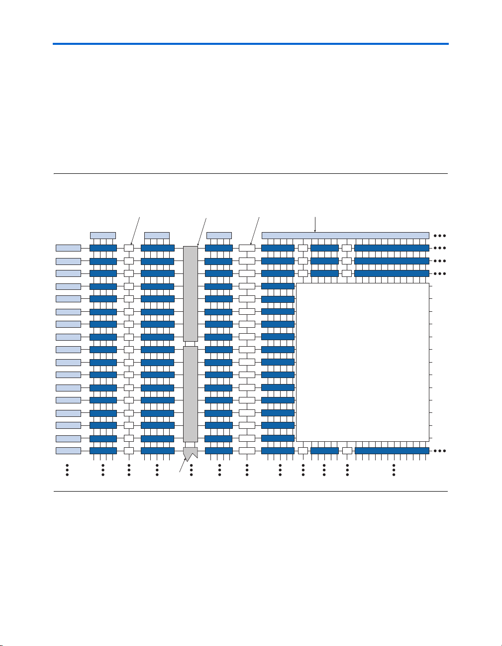
Figure 2–1 shows an overview of the Stratix device.
Figure 2–1. Stratix Block Diagram
M512 RAM Blocks for
Dual-Port Memory, Shift
Registers, & FIFO Buffers
DSP Blocks for
Multiplication and Full
Implementation of FIR Filters
M4K RAM Blocks
for True Dual-Port
Memory & Other Embedded
Memory Functions
IOEs Support DDR, PCI, GTL+, SSTL-3,
SSTL-2, HSTL, LVDS, LVPECL, PCML,
HyperTransport & other I/O Standards
IOEs
IOEs
IOEs
IOEs
IOEs
IOEs
IOEs
IOEs
IOEs
IOEs
IOEs
IOEs
IOEs
IOEs
IOEs
IOEs
IOEs
IOEs
LABs
LABs
LABs
LABs
LABs
LABs
LABs
LABs
LABs
LABs
LABs
LABs
LABs
LABs
LABs
LABs
LABs
IOEs
LABs
LABs
LABs
LABs
LABs
LABs
LABs
LABs
LABs
LABs
LABs
LABs
LABs
LABs
LABs
LABs
LABs
DSP
Block
IOEs IOEs
LABs LABs
LABs
LABs LABs
LABs
LABs
LABs
LABs
LABs
LABs
LABs
LABs
LABs
LABs
LABs
LABs
LABs
LABs LABs
LABs
LABs
LABs
LABs
LABs
LABs
LABs
LABs
LABs
LABs
LABs
LABs
LABs
LABs
LABs
LABs
LABs
LABs
LABs
LABs
LABs
LABs
LABs
LABs
M-RAM Block
2–2 Altera Corporation
Stratix Device Handbook, Volume 1 July 2005
Page 27
The number of M512 RAM, M4K RAM, and DSP blocks varies by device
along with row and column numbers and M-RAM blocks. Table 2–1 lists
the resources available in Stratix devices.
Table 2–1. Stratix Device Resources
Stratix Architecture
Device
EP1S10 4 / 94 2 / 60 1 2 / 6 40 30
EP1S20 6 / 194 2 / 82 2 2 / 10 52 41
EP1S25 6 / 224 3 / 138 2 2 / 10 62 46
EP1S30 7 / 295 3 / 171 4 2 / 12 67 57
EP1S40 8 / 384 3 / 183 4 2 / 14 77 61
EP1S60 10 / 574 4 / 292 6 2 / 18 90 73
EP1S80 11 / 767 4 / 364 9 2 / 22 101 91
M512 RAM
Columns/Blocks
Logic Array Blocks
M4K RAM
Columns/Blocks
M-RAM
Blocks
DSP Block
Columns/Blocks
LAB
Columns
LAB Rows
Each LAB consists of 10 LEs, LE carry chains, LAB control signals, local
interconnect, LUT chain, and register chain connection lines. The local
interconnect transfers signals between LEs in the same LAB. LUT chain
connections transfer the output of one LE’s LUT to the adjacent LE for fast
sequential LUT connections within the same LAB. Register chain
connections transfer the output of one LE’s register to the adjacent LE’s
®
register within an LAB. The Quartus
II Compiler places associated logic
within an LAB or adjacent LABs, allowing the use of local, LUT chain,
and register chain connections for performance and area efficiency.
Figure 2–2 shows the Stratix LAB.
Altera Corporation 2–3
July 2005 Stratix Device Handbook, Volume 1
Page 28
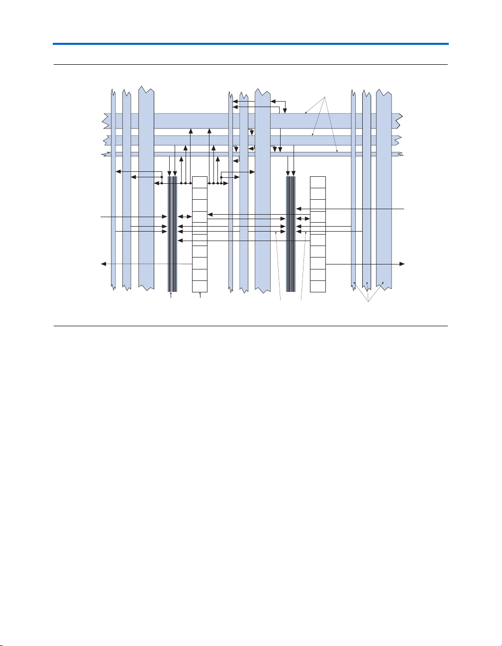
Logic Array Blocks
Figure 2–2. Stratix LAB Structure
Direct link
interconnect from
adjacent block
Row Interconnects of
Variable Speed & Length
Direct link
interconnect from
adjacent block
Direct link
interconnect to
adjacent block
Direct link
interconnect to
adjacent block
Local Interconnect
LAB
Three-Sided Architecture—Local
Interconnect is Driven from Either Side by
Columns & LABs, & from Above by Rows
Column Interconnects of
Variable Speed & Length
LAB Interconnects
The LAB local interconnect can drive LEs within the same LAB. The LAB
local interconnect is driven by column and row interconnects and LE
outputs within the same LAB. Neighboring LABs, M512 RAM blocks,
M4K RAM blocks, or DSP blocks from the left and right can also drive an
LAB’s local interconnect through the direct link connection. The direct
link connection feature minimizes the use of row and column
interconnects, providing higher performance and flexibility. Each LE can
drive 30 other LEs through fast local and direct link interconnects.
Figure 2–3 shows the direct link connection.
2–4 Altera Corporation
Stratix Device Handbook, Volume 1 July 2005
Page 29
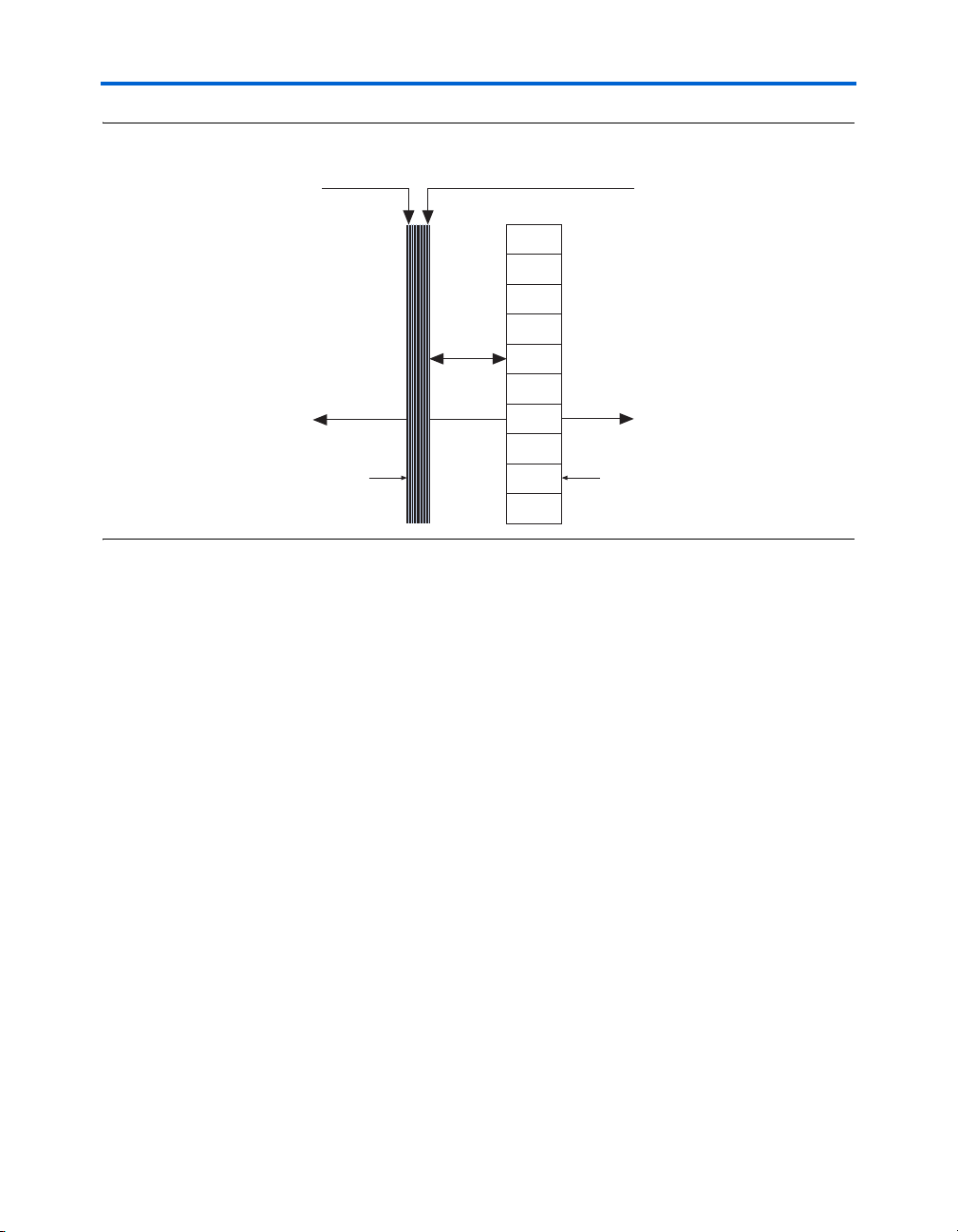
Figure 2–3. Direct Link Connection
Stratix Architecture
Direct link interconnect from
left LAB, TriMatrix memory
block, DSP block, or IOE output
Direct link
interconnect
to left
Interconnect
Direct link interconnect from
right LAB, TriMatrix memory
block, DSP block, or IOE output
Direct link
interconnect
to right
Local
LAB
LAB Control Signals
Each LAB contains dedicated logic for driving control signals to its LEs.
The control signals include two clocks, two clock enables, two
asynchronous clears, synchronous clear, asynchronous preset/load,
synchronous load, and add/subtract control signals. This gives a
maximum of 10 control signals at a time. Although synchronous load and
clear signals are generally used when implementing counters, they can
also be used with other functions.
Each LAB can use two clocks and two clock enable signals. Each LAB’s
clock and clock enable signals are linked. For example, any LE in a
particular LAB using the labclk1 signal will also use labclkena1. If
the LAB uses both the rising and falling edges of a clock, it also uses both
LAB-wide clock signals. De-asserting the clock enable signal will turn off
the LAB-wide clock.
Each LAB can use two asynchronous clear signals and an asynchronous
load/preset signal. The asynchronous load acts as a preset when the
asynchronous load data input is tied high.
Altera Corporation 2–5
July 2005 Stratix Device Handbook, Volume 1
Page 30
Logic Elements
With the LAB-wide addnsub control signal, a single LE can implement a
one-bit adder and subtractor. This saves LE resources and improves
performance for logic functions such as DSP correlators and signed
multipliers that alternate between addition and subtraction depending
on data.
The LAB row clocks [7..0] and LAB local interconnect generate the LABwide control signals. The MultiTrack
allows clock and control signal distribution in addition to data. Figure 2–4
shows the LAB control signal generation circuit.
Figure 2–4. LAB-Wide Control Signals
Dedicated
Row LAB
Clocks
Local
Interconnect
Local
Interconnect
Local
Interconnect
Local
Interconnect
Local
Interconnect
Local
Interconnect
Logic Elements
8
The smallest unit of logic in the Stratix architecture, the LE, is compact
and provides advanced features with efficient logic utilization. Each LE
contains a four-input LUT, which is a function generator that can
implement any function of four variables. In addition, each LE contains a
programmable register and carry chain with carry select capability. A
single LE also supports dynamic single bit addition or subtraction mode
selectable by an LAB-wide control signal. Each LE drives all types of
interconnects: local, row, column, LUT chain, register chain, and direct
link interconnects. See Figure 2–5.
labclkena1
TM
interconnect’s inherent low skew
labclkena2
labclk2labclk1
asyncload
or labpre
syncload
labclr1
labclr2
addnsub
synclr
2–6 Altera Corporation
Stratix Device Handbook, Volume 1 July 2005
Page 31

Figure 2–5. Stratix LE
LAB Carry-In
addnsub
data1
data2
data3
data4
labclr1
labclr2
labpre/aload
Chip-Wide
Reset
labclk1
labclk2
Asynchronous
Clear/Preset/
Load Logic
Clock &
Clock Enable
Select
Carry-In1
Carry-In0
Look-Up
Tabl e
(LUT)
Carry
Chain
Register chain
routing from
previous LE
Synchronous
LAB-wide
Load
Synchronous
Synchronous
Load and
Clear Logic
LAB-wide
Clear
Register Bypass
Packed
Register Select
PRN/ALD
D
ADATA
ENA
CLRN
Register
Feedback
Stratix Architecture
Programmable
Register
LUT chain
routing to next LE
Row, column,
Q
and direct link
routing
Row, column,
and direct link
routing
Local Routing
Register chain
output
labclkena1
labclkena2
Carry-Out0
Carry-Out1
LAB Carry-Out
Each LE’s programmable register can be configured for D, T, JK, or SR
operation. Each register has data, true asynchronous load data, clock,
clock enable, clear, and asynchronous load/preset inputs. Global signals,
general-purpose I/O pins, or any internal logic can drive the register’s
clock and clear control signals. Either general-purpose I/O pins or
internal logic can drive the clock enable, preset, asynchronous load, and
asynchronous data. The asynchronous load data input comes from the
data3 input of the LE. For combinatorial functions, the register is
bypassed and the output of the LUT drives directly to the outputs of the
LE.
Each LE has three outputs that drive the local, row, and column routing
resources. The LUT or register output can drive these three outputs
independently. Two LE outputs drive column or row and direct link
routing connections and one drives local interconnect resources. This
allows the LUT to drive one output while the register drives another
output. This feature, called register packing, improves device utilization
because the device can use the register and the LUT for unrelated
Altera Corporation 2–7
July 2005 Stratix Device Handbook, Volume 1
Page 32

Logic Elements
functions. Another special packing mode allows the register output to
feed back into the LUT of the same LE so that the register is packed with
its own fan-out LUT. This provides another mechanism for improved
fitting. The LE can also drive out registered and unregistered versions of
the LUT output.
LUT Chain & Register Chain
In addition to the three general routing outputs, the LEs within an LAB
have LUT chain and register chain outputs. LUT chain connections allow
LUTs within the same LAB to cascade together for wide input functions.
Register chain outputs allow registers within the same LAB to cascade
together. The register chain output allows an LAB to use LUTs for a single
combinatorial function and the registers to be used for an unrelated shift
register implementation. These resources speed up connections between
LABs while saving local interconnect resources. See “MultiTrack
Interconnect” on page 2–14 for more information on LUT chain and
register chain connections.
addnsub Signal
The LE’s dynamic adder/subtractor feature saves logic resources by
using one set of LEs to implement both an adder and a subtractor. This
feature is controlled by the LAB-wide control signal addnsub. The
addnsub signal sets the LAB to perform either A + B or A – B. The LUT
computes addition, and subtraction is computed by adding the two’s
complement of the intended subtractor. The LAB-wide signal converts to
two’s complement by inverting the B bits within the LAB and setting
carry-in = 1 to add one to the least significant bit (LSB). The LSB of an
adder/subtractor must be placed in the first LE of the LAB, where the
LAB-wide addnsub signal automatically sets the carry-in to 1. The
Quartus II Compiler automatically places and uses the adder/subtractor
feature when using adder/subtractor parameterized functions.
LE Operating Modes
The Stratix LE can operate in one of the following modes:
■ Normal mode
■ Dynamic arithmetic mode
Each mode uses LE resources differently. In each mode, eight available
inputs to the LE—the four data inputs from the LAB local interconnect;
carry-in0 and carry-in1 from the previous LE; the LAB carry-in
from the previous carry-chain LAB; and the register chain connection—
are directed to different destinations to implement the desired logic
function. LAB-wide signals provide clock, asynchronous clear,
2–8 Altera Corporation
Stratix Device Handbook, Volume 1 July 2005
Page 33

Stratix Architecture
asynchronous preset load, synchronous clear, synchronous load, and
clock enable control for the register. These LAB-wide signals are available
in all LE modes. The addnsub control signal is allowed in arithmetic
mode.
The Quartus II software, in conjunction with parameterized functions
such as library of parameterized modules (LPM) functions, automatically
chooses the appropriate mode for common functions such as counters,
adders, subtractors, and arithmetic functions. If required, you can also
create special-purpose functions that specify which LE operating mode to
use for optimal performance.
Normal Mode
The normal mode is suitable for general logic applications and
combinatorial functions. In normal mode, four data inputs from the LAB
local interconnect are inputs to a four-input LUT (see Figure 2–6). The
Quartus II Compiler automatically selects the carry-in or the data3
signal as one of the inputs to the LUT. Each LE can use LUT chain
connections to drive its combinatorial output directly to the next LE in the
LAB. Asynchronous load data for the register comes from the data3
input of the LE. LEs in normal mode support packed registers.
Figure 2–6. LE in Normal Mode
sclear
(LAB Wide)
addnsub (LAB Wide)
(1)
data1
data2
data3
cin (from cout
of previous LE)
data4
4-Input
LUT
Register Feedback
Register chain
connection
sload
(LAB Wide)
clock (LAB Wide)
ena (LAB Wide)
aclr (LAB Wide)
Note to Figure 2–6:
(1) This signal is only allowed in normal mode if the LE is at the end of an adder/subtractor chain.
Altera Corporation 2–9
July 2005 Stratix Device Handbook, Volume 1
aload
(LAB Wide)
ALD/PRE
ADATA
D
ENA
CLRN
Q
Row, column, and
direct link routing
Row, column, and
direct link routing
Local routing
LUT chain
connection
Register
chain output
Page 34

Logic Elements
Dynamic Arithmetic Mode
The dynamic arithmetic mode is ideal for implementing adders, counters,
accumulators, wide parity functions, and comparators. An LE in dynamic
arithmetic mode uses four 2-input LUTs configurable as a dynamic
adder/subtractor. The first two 2-input LUTs compute two summations
based on a possible carry-in of 1 or 0; the other two LUTs generate carry
outputs for the two chains of the carry select circuitry. As shown in
Figure 2–7, the LAB carry-in signal selects either the carry-in0 or
carry-in1 chain. The selected chain’s logic level in turn determines
which parallel sum is generated as a combinatorial or registered output.
For example, when implementing an adder, the sum output is the
selection of two possible calculated sums: data1 + data2 + carry-in0
or data1 + data2 + carry-in1. The other two LUTs use the data1 and
data2 signals to generate two possible carry-out signals—one for a carry
of 1 and the other for a carry of 0. The carry-in0 signal acts as the carry
select for the carry-out0 output and carry-in1 acts as the carry select
for the carry-out1 output. LEs in arithmetic mode can drive out
registered and unregistered versions of the LUT output.
The dynamic arithmetic mode also offers clock enable, counter enable,
synchronous up/down control, synchronous clear, synchronous load,
and dynamic adder/subtractor options. The LAB local interconnect data
inputs generate the counter enable and synchronous up/down control
signals. The synchronous clear and synchronous load options are LABwide signals that affect all registers in the LAB. The Quartus II software
automatically places any registers that are not used by the counter into
other LABs. The addnsub LAB-wide signal controls whether the LE acts
as an adder or subtractor.
2–10 Altera Corporation
Stratix Device Handbook, Volume 1 July 2005
Page 35

Figure 2–7. LE in Dynamic Arithmetic Mode
LAB Carry-In
Carry-In0
Carry-In1
addnsub
(LAB Wide)
(1)
Register chain
connection
sload
(LAB Wide)
sclear
(LAB Wide)
aload
(LAB Wide)
Stratix Architecture
data1
data2
data3
LUT
LUT
LUT
LUT
clock (LAB Wide)
ena (LAB Wide)
aclr (LAB Wide)
Register Feedback
Carry-Out1Carry-Out0
ALD/PRE
ADATA
D
ENA
CLRN
Note to Figure 2–7:
(1) The addnsub signal is tied to the carry input for the first LE of a carry chain only.
Carry-Select Chain
The carry-select chain provides a very fast carry-select function between
LEs in arithmetic mode. The carry-select chain uses the redundant carry
calculation to increase the speed of carry functions. The LE is configured
to calculate outputs for a possible carry-in of 1 and carry-in of 0 in
parallel. The carry-in0 and carry-in1 signals from a lower-order bit
feed forward into the higher-order bit via the parallel carry chain and feed
into both the LUT and the next portion of the carry chain. Carry-select
chains can begin in any LE within an LAB.
Q
Row, column, and
direct link routing
Row, column, and
direct link routing
Local routing
LUT chain
connection
Register
chain output
The speed advantage of the carry-select chain is in the parallel precomputation of carry chains. Since the LAB carry-in selects the
precomputed carry chain, not every LE is in the critical path. Only the
propagation delay between LAB carry-in generation (LE 5 and LE 10) are
now part of the critical path. This feature allows the Stratix architecture to
implement high-speed counters, adders, multipliers, parity functions,
and comparators of arbitrary width.
Altera Corporation 2–11
July 2005 Stratix Device Handbook, Volume 1
Page 36

Logic Elements
Figure 2–8 shows the carry-select circuitry in an LAB for a 10-bit full
adder. One portion of the LUT generates the sum of two bits using the
input signals and the appropriate carry-in bit; the sum is routed to the
output of the LE. The register can be bypassed for simple adders or used
for accumulator functions. Another portion of the LUT generates carryout bits. An LAB-wide carry in bit selects which chain is used for the
addition of given inputs. The carry-in signal for each chain, carry-in0
or carry-in1, selects the carry-out to carry forward to the carry-in
signal of the next-higher-order bit. The final carry-out signal is routed to
an LE, where it is fed to local, row, or column interconnects.
The Quartus II Compiler automatically creates carry chain logic during
design processing, or you can create it manually during design entry.
Parameterized functions such as LPM functions automatically take
advantage of carry chains for the appropriate functions.
The Quartus II Compiler creates carry chains longer than 10 LEs by
linking LABs together automatically. For enhanced fitting, a long carry
chain runs vertically allowing fast horizontal connections to TriMatrix
™
memory and DSP blocks. A carry chain can continue as far as a full
column.
2–12 Altera Corporation
Stratix Device Handbook, Volume 1 July 2005
Page 37

Figure 2–8. Carry Select Chain
Stratix Architecture
LAB Carry-In
A1
B1
A2
B2
A3
B3
A4
B4
A5
B5
A6
B6
A7
B7
A8
B8
A9
B9
01
LE1
LE2
LE3
LE4
LE5
01
LE6
LE7
LE8
LE9
Sum1
Sum2
Sum3
Sum4
Sum5
Sum6
Sum7
Sum8
Sum9
LAB Carry-In
Carry-In0
Carry-In1
data1
data2
LUT
Sum
LUT
LUT
LUT
Carry-Out0 Carry-Out1
A10
B10
LAB Carry-Out
LE10
Sum10
Clear & Preset Logic Control
LAB-wide signals control the logic for the register’s clear and preset
signals. The LE directly supports an asynchronous clear and preset
function. The register preset is achieved through the asynchronous load
of a logic high. The direct asynchronous preset does not require a NOTgate push-back technique. Stratix devices support simultaneous preset/
Altera Corporation 2–13
July 2005 Stratix Device Handbook, Volume 1
Page 38

MultiTrack Interconnect
asynchronous load, and clear signals. An asynchronous clear signal takes
precedence if both signals are asserted simultaneously. Each LAB
supports up to two clears and one preset signal.
In addition to the clear and preset ports, Stratix devices provide a chipwide reset pin (DEV_CLRn) that resets all registers in the device. An
option set before compilation in the Quartus II software controls this pin.
This chip-wide reset overrides all other control signals.
MultiTrack
Interconnect
In the Stratix architecture, connections between LEs, TriMatrix memory,
DSP blocks, and device I/O pins are provided by the MultiTrack
interconnect structure with DirectDriveTM technology. The MultiTrack
interconnect consists of continuous, performance-optimized routing lines
of different lengths and speeds used for inter- and intra-design block
connectivity. The Quartus II Compiler automatically places critical design
paths on faster interconnects to improve design performance.
DirectDrive technology is a deterministic routing technology that ensures
identical routing resource usage for any function regardless of placement
within the device. The MultiTrack interconnect and DirectDrive
technology simplify the integration stage of block-based designing by
eliminating the re-optimization cycles that typically follow design
changes and additions.
The MultiTrack interconnect consists of row and column interconnects
that span fixed distances. A routing structure with fixed length resources
for all devices allows predictable and repeatable performance when
migrating through different device densities. Dedicated row
interconnects route signals to and from LABs, DSP blocks, and TriMatrix
memory within the same row. These row resources include:
■ Direct link interconnects between LABs and adjacent blocks.
■ R4 interconnects traversing four blocks to the right or left.
■ R8 interconnects traversing eight blocks to the right or left.
■ R24 row interconnects for high-speed access across the length of the
device.
The direct link interconnect allows an LAB, DSP block, or TriMatrix
memory block to drive into the local interconnect of its left and right
neighbors and then back into itself. Only one side of a M-RAM block
interfaces with direct link and row interconnects. This provides fast
communication between adjacent LABs and/or blocks without using row
interconnect resources.
The R4 interconnects span four LABs, three LABs and one M512 RAM
block, two LABs and one M4K RAM block, or two LABs and one DSP
block to the right or left of a source LAB. These resources are used for fast
2–14 Altera Corporation
Stratix Device Handbook, Volume 1 July 2005
Page 39

row connections in a four-LAB region. Every LAB has its own set of R4
interconnects to drive either left or right. Figure 2–9 shows R4
interconnect connections from an LAB. R4 interconnects can drive and be
driven by DSP blocks and RAM blocks and horizontal IOEs. For LAB
interfacing, a primary LAB or LAB neighbor can drive a given R4
interconnect. For R4 interconnects that drive to the right, the primary
LAB and right neighbor can drive on to the interconnect. For R4
interconnects that drive to the left, the primary LAB and its left neighbor
can drive on to the interconnect. R4 interconnects can drive other R4
interconnects to extend the range of LABs they can drive. R4
interconnects can also drive C4 and C16 interconnects for connections
from one row to another. Additionally, R4 interconnects can drive R24
interconnects.
Figure 2–9. R4 Interconnect Connections
Adjacent LAB can
Drive onto Another
LAB's R4 Interconnect
R4 Interconnect
Driving Left
C4, C8, and C16
Column Interconnects (1)
R4 Interconnect
Driving Right
Stratix Architecture
LAB
Neighbor
Primary
LAB (2)
LAB
Neighbor
Notes to Figure 2–9:
(1) C4 interconnects can drive R4 interconnects.
(2) This pattern is repeated for every LAB in the LAB row.
The R8 interconnects span eight LABs, M512 or M4K RAM blocks, or DSP
blocks to the right or left from a source LAB. These resources are used for
fast row connections in an eight-LAB region. Every LAB has its own set
of R8 interconnects to drive either left or right. R8 interconnect
connections between LABs in a row are similar to the R4 connections
shown in Figure 2–9, with the exception that they connect to eight LABs
to the right or left, not four. Like R4 interconnects, R8 interconnects can
drive and be driven by all types of architecture blocks. R8 interconnects
Altera Corporation 2–15
July 2005 Stratix Device Handbook, Volume 1
Page 40

MultiTrack Interconnect
can drive other R8 interconnects to extend their range as well as C8
interconnects for row-to-row connections. One R8 interconnect is faster
than two R4 interconnects connected together.
R24 row interconnects span 24 LABs and provide the fastest resource for
long row connections between LABs, TriMatrix memory, DSP blocks, and
IOEs. The R24 row interconnects can cross M-RAM blocks. R24 row
interconnects drive to other row or column interconnects at every fourth
LAB and do not drive directly to LAB local interconnects. R24 row
interconnects drive LAB local interconnects via R4 and C4 interconnects.
R24 interconnects can drive R24, R4, C16, and C4 interconnects.
The column interconnect operates similarly to the row interconnect and
vertically routes signals to and from LABs, TriMatrix memory, DSP
blocks, and IOEs. Each column of LABs is served by a dedicated column
interconnect, which vertically routes signals to and from LABs, TriMatrix
memory and DSP blocks, and horizontal IOEs. These column resources
include:
■ LUT chain interconnects within an LAB
■ Register chain interconnects within an LAB
■ C4 interconnects traversing a distance of four blocks in up and down
direction
■ C8 interconnects traversing a distance of eight blocks in up and
down direction
■ C16 column interconnects for high-speed vertical routing through
the device
Stratix devices include an enhanced interconnect structure within LABs
for routing LE output to LE input connections faster using LUT chain
connections and register chain connections. The LUT chain connection
allows the combinatorial output of an LE to directly drive the fast input
of the LE right below it, bypassing the local interconnect. These resources
can be used as a high-speed connection for wide fan-in functions from
LE 1 to LE 10 in the same LAB. The register chain connection allows the
register output of one LE to connect directly to the register input of the
next LE in the LAB for fast shift registers. The Quartus II Compiler
automatically takes advantage of these resources to improve utilization
and performance. Figure 2–10 shows the LUT chain and register chain
interconnects.
2–16 Altera Corporation
Stratix Device Handbook, Volume 1 July 2005
Page 41

Figure 2–10. LUT Chain & Register Chain Interconnects
t
Local Interconnect
Routing Among LEs
in the LAB
Stratix Architecture
LUT Chain
Routing to
Adjacent LE
Local
Interconnect
LE 1
LE 2
LE 3
LE 4
LE 5
LE 6
LE 7
LE 8
LE 9
LE 10
Register Chain
Routing to Adjacen
LE's Register Input
The C4 interconnects span four LABs, M512, or M4K blocks up or down
from a source LAB. Every LAB has its own set of C4 interconnects to drive
either up or down. Figure 2–11 shows the C4 interconnect connections
from an LAB in a column. The C4 interconnects can drive and be driven
by all types of architecture blocks, including DSP blocks, TriMatrix
memory blocks, and vertical IOEs. For LAB interconnection, a primary
LAB or its LAB neighbor can drive a given C4 interconnect.
C4 interconnects can drive each other to extend their range as well as
drive row interconnects for column-to-column connections.
Altera Corporation 2–17
July 2005 Stratix Device Handbook, Volume 1
Page 42

MultiTrack Interconnect
4
Figure 2–11. C4 Interconnect Connections Note (1)
C4 Interconnect
Drives Local and R
Interconnects
up to Four Rows
C4 Interconnect
Driving Up
LAB
Row
Interconnect
Adjacent LAB can
drive onto neighboring
LAB's C4 interconnect
Local
Interconnect
C4 Interconnect
Driving Down
Note to Figure 2–11:
(1) Each C4 interconnect can drive either up or down four rows.
2–18 Altera Corporation
Stratix Device Handbook, Volume 1 July 2005
Page 43

Stratix Architecture
C8 interconnects span eight LABs, M512, or M4K blocks up or down from
a source LAB. Every LAB has its own set of C8 interconnects to drive
either up or down. C8 interconnect connections between the LABs in a
column are similar to the C4 connections shown in Figure 2–11 with the
exception that they connect to eight LABs above and below. The C8
interconnects can drive and be driven by all types of architecture blocks
similar to C4 interconnects. C8 interconnects can drive each other to
extend their range as well as R8 interconnects for column-to-column
connections. C8 interconnects are faster than two C4 interconnects.
C16 column interconnects span a length of 16 LABs and provide the
fastest resource for long column connections between LABs, TriMatrix
memory blocks, DSP blocks, and IOEs. C16 interconnects can cross MRAM blocks and also drive to row and column interconnects at every
fourth LAB. C16 interconnects drive LAB local interconnects via C4 and
R4 interconnects and do not drive LAB local interconnects directly.
All embedded blocks communicate with the logic array similar to LABto-LAB interfaces. Each block (i.e., TriMatrix memory and DSP blocks)
connects to row and column interconnects and has local interconnect
regions driven by row and column interconnects. These blocks also have
direct link interconnects for fast connections to and from a neighboring
LAB. All blocks are fed by the row LAB clocks, labclk[7..0].
Altera Corporation 2–19
July 2005 Stratix Device Handbook, Volume 1
Page 44

MultiTrack Interconnect
Table 2–2 shows the Stratix device’s routing scheme.
Table 2–2. Stratix Device Routing Scheme
Source
LUT Chain
Register Chain
Local Interconnect
Direct Link Interconnect
LUT Chain
Register Chain
Local
Interconnect
Direct Link
Interconnect
R4 Interconnect
R8 Interconnect
R24
Interconnect
C4 Interconnect
C8 Interconnect
C16
Interconnect
LE
M512 RAM
Block
M4K RAM Block
M-RAM Block
DSP Blocks
Column IOE
Row IOE
vvvvvv vv
v
vvvvv
vvv
vv v
vvv
vvvv vv
vvvv vv
vvvv vv
vvvv
v vvvvv
Destination
R4 Interconnect
R8 Interconnect
R24 Interconnect
C4 Interconnect
C8 Interconnect
C16 Interconnect
LE
v
v
vvvvvvv
vvvv
vvvv
vv
M512 RAM Block
M4K RAM Block
M-RAM Block
DSP Blocks
Column IOE
Row IOE
2–20 Altera Corporation
Stratix Device Handbook, Volume 1 July 2005
Page 45

Stratix Architecture
TriMatrix Memory
TriMatrix memory consists of three types of RAM blocks: M512, M4K,
and M-RAM blocks. Although these memory blocks are different, they
can all implement various types of memory with or without parity,
including true dual-port, simple dual-port, and single-port RAM, ROM,
and FIFO buffers. Table 2–3 shows the size and features of the different
RAM blocks.
Table 2–3. TriMatrix Memory Features (Part 1 of 2)
Memory Feature
Maximum
performance
True dual-port
memory
Simple dual-port
memory
Single-port memory
Shift register
ROM
FIFO buffer
Byte enable
Parity bits
Mixed clock mode
Memory initialization
Simple dual-port
memory mixed width
support
True dual-port
memory mixed width
support
Power-up conditions Outputs cleared Outputs cleared Outputs
Register clears Input and output
Mixed-port readduring-write
M512 RAM Block
(32 × 18 Bits)
(1) (1) (1)
vvv
vvv
vv
vv
vvv
vvv
vvv
vv
vvv
registers
Unknown
output/old data
M4K RAM Block
(128×36Bits)
M-RAM Block
(4K × 144 Bits)
vv
(2)
vv
vv
unknown
Input and output
registers
Unknown
output/old data
Output registers
Unknown output
Altera Corporation 2–21
July 2005 Stratix Device Handbook, Volume 1
Page 46

Tri M a t r ix Memo r y
Table 2–3. TriMatrix Memory Features (Part 2 of 2)
Memory Feature
M512 RAM Block
(32 × 18 Bits)
Configurations 512 × 1
256 × 2
128 × 4
64 × 8
64 × 9
32 × 16
32 × 18
M4K RAM Block
(128×36Bits)
4K × 1
2K × 2
1K × 4
512 × 8
512 × 9
256 × 16
256 × 18
128 × 32
128 × 36
M-RAM Block
(4K × 144 Bits)
64K × 8
64K × 9
32K × 16
32K × 18
16K × 32
16K × 36
8K × 64
8K × 72
4K × 128
4K × 144
Notes to Ta b l e 2 – 3:
(1) See Table 4–36 for maximum performance information.
(2) The M-RAM block does not support memory initializations. However, the
M-RAM block can emulate a ROM function using a dual-port RAM bock. The
Stratix device must write to the dual-port memory once and then disable the
write-enable ports afterwards.
1 Violating the setup or hold time on the address registers could
corrupt the memory contents. This applies to both read and
write operations.
Memory Modes
TriMatrix memory blocks include input registers that synchronize writes
and output registers to pipeline designs and improve system
performance. M4K and M-RAM memory blocks offer a true dual-port
mode to support any combination of two-port operations: two reads, two
writes, or one read and one write at two different clock frequencies.
Figure 2–12 shows true dual-port memory.
Figure 2–12. True Dual-Port Memory Configuration
AB
dataA[ ]
[ ]
address
A
wren
A
clock
A
clocken
A
qA[ ]
aclr
A
2–22 Altera Corporation
Stratix Device Handbook, Volume 1 July 2005
dataB[ ]
address
wren
clockB
clocken
aclr
qB[ ]
[ ]
B
B
B
B
Page 47

Stratix Architecture
In addition to true dual-port memory, the memory blocks support simple
dual-port and single-port RAM. Simple dual-port memory supports a
simultaneous read and write and can either read old data before the write
occurs or just read the don’t care bits. Single-port memory supports nonsimultaneous reads and writes, but the q[] port will output the data once
it has been written to the memory (if the outputs are not registered) or
after the next rising edge of the clock (if the outputs are registered). For
more information, see Chapter 2, TriMatrix Embedded Memory Blocks in
Stratix & Stratix GX Devices of the Stratix Device Handbook, Volume 2.
Figure 2–13 shows these different RAM memory port configurations for
TriMatrix memory.
Figure 2–13. Simple Dual-Port & Single-Port Memory Configurations
Simple Dual-Port Memory
data[ ]
wraddress[ ]
wren
inclock
inclocken
inaclr
rdaddress[ ]
rden
q[ ]
outclock
outclocken
outaclr
Single-Port Memory (1)
data[ ]
address[ ]
wren
inclock
inclocken
inaclr
q[ ]
outclock
outclocken
outaclr
Note to Figure 2–13:
(1) Two single-port memory blocks can be implemented in a single M4K block as long
as each of the two independent block sizes is equal to or less than half of the M4K
block size.
The memory blocks also enable mixed-width data ports for reading and
writing to the RAM ports in dual-port RAM configuration. For example,
the memory block can be written in ×1 mode at port A and read out in ×16
mode from port B.
Altera Corporation 2–23
July 2005 Stratix Device Handbook, Volume 1
Page 48

Tri M a t r ix Memo r y
TriMatrix memory architecture can implement pipelined RAM by
registering both the input and output signals to the RAM block. All
TriMatrix memory block inputs are registered providing synchronous
write cycles. In synchronous operation, the memory block generates its
own self-timed strobe write enable (WREN) signal derived from the global
or regional clock. In contrast, a circuit using asynchronous RAM must
generate the RAM WREN signal while ensuring its data and address
signals meet setup and hold time specifications relative to the WREN
signal. The output registers can be bypassed. Flow-through reading is
possible in the simple dual-port mode of M512 and M4K RAM blocks by
clocking the read enable and read address registers on the negative clock
edge and bypassing the output registers.
Two single-port memory blocks can be implemented in a single M4K
block as long as each of the two independent block sizes is equal to or less
than half of the M4K block size.
The Quartus II software automatically implements larger memory by
combining multiple TriMatrix memory blocks. For example, two
256 × 16-bit RAM blocks can be combined to form a 256 × 32-bit RAM
block. Memory performance does not degrade for memory blocks using
the maximum number of words available in one memory block. Logical
memory blocks using less than the maximum number of words use
physical blocks in parallel, eliminating any external control logic that
would increase delays. To create a larger high-speed memory block, the
Quartus II software automatically combines memory blocks with LE
control logic.
Clear Signals
When applied to input registers, the asynchronous clear signal for the
TriMatrix embedded memory immediately clears the input registers.
However, the output of the memory block does not show the effects until
the next clock edge. When applied to output registers, the asynchronous
clear signal clears the output registers and the effects are seen
immediately.
Parity Bit Support
The memory blocks support a parity bit for each byte. The parity bit,
along with internal LE logic, can implement parity checking for error
detection to ensure data integrity. You can also use parity-size data words
to store user-specified control bits. In the M4K and M-RAM blocks, byte
enables are also available for data input masking during write operations.
2–24 Altera Corporation
Stratix Device Handbook, Volume 1 July 2005
Page 49

Stratix Architecture
Shift Register Support
You can configure embedded memory blocks to implement shift registers
for DSP applications such as pseudo-random number generators, multichannel filtering, auto-correlation, and cross-correlation functions. These
and other DSP applications require local data storage, traditionally
implemented with standard flip-flops, which can quickly consume many
logic cells and routing resources for large shift registers. A more efficient
alternative is to use embedded memory as a shift register block, which
saves logic cell and routing resources and provides a more efficient
implementation with the dedicated circuitry.
The size of a w × m × n shift register is determined by the input data
width (w), the length of the taps (m), and the number of taps (n). The size
of a w × m × n shift register must be less than or equal to the maximum
number of memory bits in the respective block: 576 bits for the M512
RAM block and 4,608 bits for the M4K RAM block. The total number of
shift register outputs (number of taps n × width w) must be less than the
maximum data width of the RAM block (18 for M512 blocks, 36 for M4K
blocks). To create larger shift registers, the memory blocks are cascaded
together.
Data is written into each address location at the falling edge of the clock
and read from the address at the rising edge of the clock. The shift register
mode logic automatically controls the positive and negative edge
clocking to shift the data in one clock cycle. Figure 2–14 shows the
TriMatrix memory block in the shift register mode.
Altera Corporation 2–25
July 2005 Stratix Device Handbook, Volume 1
Page 50

Tri M a t r ix Memo r y
r
Figure 2–14. Shift Register Memory Configuration
w × m × n Shift Register
m-Bit Shift Register
w w
m-Bit Shift Register
w
m-Bit Shift Register
w
w
n Numbe
of Taps
w
m-Bit Shift Register
w
w
Memory Block Size
TriMatrix memory provides three different memory sizes for efficient
application support. The large number of M512 blocks are ideal for
designs with many shallow first-in first-out (FIFO) buffers. M4K blocks
provide additional resources for channelized functions that do not
require large amounts of storage. The M-RAM blocks provide a large
single block of RAM ideal for data packet storage. The different-sized
blocks allow Stratix devices to efficiently support variable-sized memory
in designs.
The Quartus II software automatically partitions the user-defined
memory into the embedded memory blocks using the most efficient size
combinations. You can also manually assign the memory to a specific
block size or a mixture of block sizes.
2–26 Altera Corporation
Stratix Device Handbook, Volume 1 July 2005
Page 51

Stratix Architecture
M512 RAM Block
The M512 RAM block is a simple dual-port memory block and is useful
for implementing small FIFO buffers, DSP, and clock domain transfer
applications. Each block contains 576 RAM bits (including parity bits).
M512 RAM blocks can be configured in the following modes:
■ Simple dual-port RAM
■ Single-port RAM
■ FIFO
■ ROM
■ Shift register
When configured as RAM or ROM, you can use an initialization file to
pre-load the memory contents.
The memory address depths and output widths can be configured as
512 × 1, 256 × 2, 128 × 4, 64 × 8 (64 × 9 bits with parity), and 32 × 16
(32 × 18 bits with parity). Mixed-width configurations are also possible,
allowing different read and write widths. Table 2–4 summarizes the
possible M512 RAM block configurations.
Table 2–4. M512 RAM Block Configurations (Simple Dual-Port RAM)
Read Port
Write Port
512 × 1 256 × 2 128 × 4 64 × 8 32 × 16 64 × 9 32 × 18
512 × 1
256 × 2
128 × 4
64 × 8
32 × 16
64 × 9
32 × 18
v v vvv
v v vvv
vvv v
vv v
vvv v
v
v
When the M512 RAM block is configured as a shift register block, a shift
register of size up to 576 bits is possible.
The M512 RAM block can also be configured to support serializer and
deserializer applications. By using the mixed-width support in
combination with DDR I/O standards, the block can function as a
SERDES to support low-speed serial I/O standards using global or
regional clocks. See “I/O Structure” on page 2–104 for details on
dedicated SERDES in Stratix devices.
Altera Corporation 2–27
July 2005 Stratix Device Handbook, Volume 1
Page 52

Tri M a t r ix Memo r y
M512 RAM blocks can have different clocks on its inputs and outputs.
The wren, datain, and write address registers are all clocked together
from one of the two clocks feeding the block. The read address, rden, and
output registers can be clocked by either of the two clocks driving the
block. This allows the RAM block to operate in read/write or
input/output clock modes. Only the output register can be bypassed. The
eight labclk signals or local interconnect can drive the inclock,
outclock, wren, rden, inclr, and outclr signals. Because of the
advanced interconnect between the LAB and M512 RAM blocks, LEs can
also control the wren and rden signals and the RAM clock, clock enable,
and asynchronous clear signals. Figure 2–15 shows the M512 RAM block
control signal generation logic.
The RAM blocks within Stratix devices have local interconnects to allow
LEs and interconnects to drive into RAM blocks. The M512 RAM block
local interconnect is driven by the R4, R8, C4, C8, and direct link
interconnects from adjacent LABs. The M512 RAM blocks can
communicate with LABs on either the left or right side through these row
interconnects or with LAB columns on the left or right side with the
column interconnects. Up to 10 direct link input connections to the M512
RAM block are possible from the left adjacent LABs and another
10 possible from the right adjacent LAB. M512 RAM outputs can also
connect to left and right LABs through 10 direct link interconnects. The
M512 RAM block has equal opportunity for access and performance to
and from LABs on either its left or right side. Figure 2–16 shows the M512
RAM block to logic array interface.
2–28 Altera Corporation
Stratix Device Handbook, Volume 1 July 2005
Page 53

Figure 2–15. M512 RAM Block Control Signals
Stratix Architecture
Dedicated
Row LAB
Clocks
Local
Interconnect
Local
Interconnect
Local
Interconnect
Local
Interconnect
Local
Interconnect
Local
Interconnect
Local
Interconnect
Local
Interconnect
8
inclocken
outclocken
outclockinclock
rden
wren
outclr
inclr
Altera Corporation 2–29
July 2005 Stratix Device Handbook, Volume 1
Page 54

Tri M a t r ix Memo r y
Figure 2–16. M512 RAM Block LAB Row Interface
C4 and C8
Interconnects
R4 and R8
Interconnects
Direct link
interconnect
to adjacent LAB
Direct link
interconnect
from adjacent LAB
10
2
8
Small RAM Block Local
Interconnect Region
M512 RAM
datain
Clocks
dataout
Block
Control
Signals
address
LAB Row Clocks
Direct link
interconnect
to adjacent LAB
Direct link
interconnect
from adjacent LAB
M4K RAM Blocks
The M4K RAM block includes support for true dual-port RAM. The M4K
RAM block is used to implement buffers for a wide variety of applications
such as storing processor code, implementing lookup schemes, and
implementing larger memory applications. Each block contains
4,608 RAM bits (including parity bits). M4K RAM blocks can be
configured in the following modes:
■ True dual-port RAM
■ Simple dual-port RAM
■ Single-port RAM
■ FIFO
■ ROM
■ Shift register
When configured as RAM or ROM, you can use an initialization file to
pre-load the memory contents.
2–30 Altera Corporation
Stratix Device Handbook, Volume 1 July 2005
Page 55

The memory address depths and output widths can be configured as
4,096 × 1, 2,048 × 2, 1,024 × 4, 512 × 8 (or 512 × 9 bits), 256 × 16 (or
256 × 18 bits), and 128 × 32 (or 128 × 36 bits). The 128 × 32- or 36-bit
configuration is not available in the true dual-port mode. Mixed-width
configurations are also possible, allowing different read and write
widths. Tables 2–5 and 2–6 summarize the possible M4K RAM block
configurations.
Table 2–5. M4K RAM Block Configurations (Simple Dual-Port)
Stratix Architecture
Read Port
Write Port
4K × 12K × 21K × 4 512 × 8 256 × 16 128 × 32 512 × 9 256 × 18 128 × 36
4K × 1
2K × 2
1K × 4
512 × 8
256 × 16
128 × 32
512 × 9
256 × 18
128 × 36
vvvv v v
vvvv v v
vvvv v v
vvvv v v
vvvv v v
vvvv v v
Table 2–6. M4K RAM Block Configurations (True Dual-Port)
Port A
4K × 12K × 21K × 4 512 × 8 256 × 16 512 × 9 256 × 18
4K × 1
2K × 2
1K × 4
512 × 8
256 × 16
512 × 9
256 × 18
vvvvv
vvvvv
vvvvv
vvvvv
vvvvv
vv v
vv v
vv v
Port B
vv
vv
When the M4K RAM block is configured as a shift register block, you can
create a shift register up to 4,608 bits (w × m × n).
Altera Corporation 2–31
July 2005 Stratix Device Handbook, Volume 1
Page 56

Tri M a t r ix Memo r y
M4K RAM blocks support byte writes when the write port has a data
width of 16, 18, 32, or 36 bits. The byte enables allow the input data to be
masked so the device can write to specific bytes. The unwritten bytes
retain the previous written value. Table 2–7 summarizes the byte
selection.
Table 2–7. Byte Enable for M4K Blocks Notes (1), (2)
byteena[3..0] datain ×18 datain ×36
[0] = 1 [8..0] [8..0]
[1] = 1 [17..9] [17..9]
[2] = 1 – [26..18]
[3] = 1 – [35..27]
Notes to Ta b l e 2 – 7:
(1) Any combination of byte enables is possible.
(2) Byte enables can be used in the same manner with 8-bit words, i.e., in × 16 and
× 32 modes.
The M4K RAM blocks allow for different clocks on their inputs and
outputs. Either of the two clocks feeding the block can clock M4K RAM
block registers (renwe, address, byte enable, datain, and output
registers). Only the output register can be bypassed. The eight labclk
signals or local interconnects can drive the control signals for the A and B
ports of the M4K RAM block. LEs can also control the clock_a,
clock_b, renwe_a, renwe_b, clr_a, clr_b, clocken_a, and
clocken_b signals, as shown in Figure 2–17.
The R4, R8, C4, C8, and direct link interconnects from adjacent LABs
drive the M4K RAM block local interconnect. The M4K RAM blocks can
communicate with LABs on either the left or right side through these row
resources or with LAB columns on either the right or left with the column
resources. Up to 10 direct link input connections to the M4K RAM Block
are possible from the left adjacent LABs and another 10 possible from the
right adjacent LAB. M4K RAM block outputs can also connect to left and
right LABs through 10 direct link interconnects each. Figure 2–18 shows
the M4K RAM block to logic array interface.
2–32 Altera Corporation
Stratix Device Handbook, Volume 1 July 2005
Page 57

Figure 2–17. M4K RAM Block Control Signals
Dedicated
Row LAB
Clocks
Local
Interconnect
8
Stratix Architecture
Local
Interconnect
Local
Interconnect
Local
Interconnect
Local
Interconnect
Local
Interconnect
clocken_a
renwe_aclock_a
Figure 2–18. M4K RAM Block LAB Row Interface
C4 and C8
Interconnects
Direct link
interconnect
to adjacent LAB
Direct link
interconnect
from adjacent LAB
10
Byte enable
Clocks
alcr_a
M4K RAM
Block
alcr_b
dataout
Control
Signals
renwe_b
clocken_b
clock_b
Local
Interconnect
Local
Interconnect
Local
Interconnect
Local
Interconnect
R4 and R8
Interconnects
Direct link
interconnect
to adjacent LAB
Direct link
interconnect
from adjacent LAB
datainaddress
8
M4K RAM Block Local
LAB Row Clocks
Interconnect Region
Altera Corporation 2–33
July 2005 Stratix Device Handbook, Volume 1
Page 58

Tri M a t r ix Memo r y
M-RAM Block
The largest TriMatrix memory block, the M-RAM block, is useful for
applications where a large volume of data must be stored on-chip. Each
block contains 589,824 RAM bits (including parity bits). The M-RAM
block can be configured in the following modes:
■ True dual-port RAM
■ Simple dual-port RAM
■ Single-port RAM
■ FIFO RAM
You cannot use an initialization file to initialize the contents of a M-RAM
block. All M-RAM block contents power up to an undefined value. Only
synchronous operation is supported in the M-RAM block, so all inputs
are registered. Output registers can be bypassed. The memory address
and output width can be configured as 64K × 8 (or 64K × 9 bits), 32K × 16
(or 32K × 18 bits), 16K × 32 (or 16K × 36 bits), 8K × 64 (or 8K × 72 bits), and
4K × 128 (or 4K × 144 bits). The 4K × 128 configuration is unavailable in
true dual-port mode because there are a total of 144 data output drivers
in the block. Mixed-width configurations are also possible, allowing
different read and write widths. Tables 2–8 and 2–9 summarize the
possible M-RAM block configurations:
Table 2–8. M-RAM Block Configurations (Simple Dual-Port)
Write Port
Read Port
64K × 932K × 18 16K × 36 8K × 72 4K × 144
64K × 9
32K × 18
16K × 36
8K × 72
4K × 144
2–34 Altera Corporation
Stratix Device Handbook, Volume 1 July 2005
vvvv
vvvv
vvvv
vvvv
v
Page 59

Table 2–9. M-RAM Block Configurations (True Dual-Port)
Stratix Architecture
Port A
Port B
64K × 932K × 18 16K × 36 8K × 72
64K × 9
32K × 18
16K × 36
8K × 72
vvvv
vvvv
vvvv
vvvv
The read and write operation of the memory is controlled by the WREN
signal, which sets the ports into either read or write modes. There is no
separate read enable (RE) signal.
Writing into RAM is controlled by both the WREN and byte enable
(byteena) signals for each port. The default value for the byteena
signal is high, in which case writing is controlled only by the WREN signal.
The byte enables are available for the ×18, ×36, and ×72 modes. In the
×144 simple dual-port mode, the two sets of byteena signals
(byteena_a and byteena_b) are combined to form the necessary
16 byte enables. Tables 2–10 and 2–11 summarize the byte selection.
Table 2–10. Byte Enable for M-RAM Blocks Notes (1), (2)
byteena[3..0] datain ×18 datain ×36 datain ×72
[0] = 1 [8..0] [8..0] [8..0]
[1] = 1 [17..9] [17..9] [17..9]
[2] = 1 – [26..18] [26..18]
[3] = 1 – [35..27] [35..27]
[4] = 1 – – [44..36]
[5] = 1 – – [53..45]
[6] = 1 – – [62..54]
[7] = 1 – – [71..63]
Altera Corporation 2–35
July 2005 Stratix Device Handbook, Volume 1
Page 60

Tri M a t r ix Memo r y
Table 2–11. M-RAM Combined Byte Selection for ×144 Mode Notes (1), (2)
byteena[15..0] datain ×144
[0] = 1 [8..0]
[1] = 1 [17..9]
[2] = 1 [26..18]
[3] = 1 [35..27]
[4] = 1 [44..36]
[5] = 1 [53..45]
[6] = 1 [62..54]
[7] = 1 [71..63]
[8] = 1 [80..72]
[9] = 1 [89..81]
[10] = 1 [98..90]
[11] = 1 [107..99]
[12] = 1 [116..108]
[13] = 1 [125..117]
[14] = 1 [134..126]
[15] = 1 [143..135]
Notes to Tables 2–10 and 2–11:
(1) Any combination of byte enables is possible.
(2) Byte enables can be used in the same manner with 8-bit words, i.e., in × 16, ×32,
× 64, and ×128 modes.
Similar to all RAM blocks, M-RAM blocks can have different clocks on
their inputs and outputs. All input registers—renwe, datain, address,
and byte enable registers—are clocked together from either of the two
clocks feeding the block. The output register can be bypassed. The eight
labclk signals or local interconnect can drive the control signals for the
A and B ports of the M-RAM block. LEs can also control the clock_a,
clock_b, renwe_a, renwe_b, clr_a, clr_b, clocken_a, and
clocken_b signals as shown in Figure 2–19.
2–36 Altera Corporation
Stratix Device Handbook, Volume 1 July 2005
Page 61

Figure 2–19. M-RAM Block Control Signals
Dedicated
Row LAB
Clocks
Local
Interconnect
Local
Interconnect
Local
Interconnect
Local
Interconnect
Local
Interconnect
Local
Interconnect
Local
Interconnect
Local
Interconnect
8
clocken_a
Stratix Architecture
clocken_b
clock_bclock_a
aclr_a
aclr_b
renwe_a
renwe_b
One of the M-RAM block’s horizontal sides drive the address and control
signal (clock, renwe, byteena, etc.) inputs. Typically, the horizontal side
closest to the device perimeter contains the interfaces. The one exception
is when two M-RAM blocks are paired next to each other. In this case, the
side of the M-RAM block opposite the common side of the two blocks
contains the input interface. The top and bottom sides of any M-RAM
block contain data input and output interfaces to the logic array. The top
side has 72 data inputs and 72 data outputs for port B, and the bottom side
has another 72 data inputs and 72 data outputs for port A. Figure 2–20
shows an example floorplan for the EP1S60 device and the location of the
M-RAM interfaces.
Altera Corporation 2–37
July 2005 Stratix Device Handbook, Volume 1
Page 62

Tri M a t r ix Memo r y
Figure 2–20. EP1S60 Device with M-RAM Interface Locations Note (1)
M-RAM pairs interface to
top, bottom, and side opposite
of block-to-block border.
Independent M-RAM blocks
interface to top, bottom, and side facing
device perimeter for easy access
to horizontal I/O pins.
DSP
Blocks
M-RAM
Block
M-RAM
Block
M512
Blocks
M-RAM
Block
M-RAM
Block
M4K
Blocks
LABs
M-RAM
Block
M-RAM
Block
DSP
Blocks
Note to Figure 2–20:
(1) Device shown is an EP1S60 device. The number and position of M-RAM blocks varies in other devices.
The M-RAM block local interconnect is driven by the R4, R8, C4, C8, and
direct link interconnects from adjacent LABs. For independent M-RAM
blocks, up to 10 direct link address and control signal input connections
to the M-RAM block are possible from the left adjacent LABs for M-RAM
2–38 Altera Corporation
Stratix Device Handbook, Volume 1 July 2005
Page 63

Stratix Architecture
blocks facing to the left, and another 10 possible from the right adjacent
LABs for M-RAM blocks facing to the right. For column interfacing, every
M-RAM column unit connects to the right and left column lines, allowing
each M-RAM column unit to communicate directly with three columns of
LABs. Figures 2–21 through 2–23 show the interface between the M-RAM
block and the logic array.
Altera Corporation 2–39
July 2005 Stratix Device Handbook, Volume 1
Page 64

Tri M a t r ix Memo r y
Figure 2–21. Left-Facing M-RAM to Interconnect Interface Notes (1), (2)
M512 RAM Block Columns
Row Unit Interface
Allows LAB Rows to
Drive Address and
Control Signals to
M-RAM Block
LABs in Row
M-RAM Boundary
R11
R10
R9
R8
R7
R6
R5
R4
R3
R2
R1
B1 B2 B3 B4 B5 B6
Port B
M-RAM Block
Port A
A1 A2 A3 A4 A5 A6
LABs in Column
M-RAM Boundary
Column Interface Block
Drives to and from
C4 and C8 Interconnects
Column Interface Block
Allows LAB Columns to
Drive datain and dataout to
and from M-RAM Block
LAB Interface
Blocks
Notes to Figure 2–21:
(1) Only R24 and C16 interconnects cross the M-RAM block boundaries.
(2) The right-facing M-RAM block has interface blocks on the right side, but none on the left. B1 to B6 and A1 to A6
orientation is clipped across the vertical axis for right-facing M-RAM blocks.
2–40 Altera Corporation
Stratix Device Handbook, Volume 1 July 2005
Page 65

Figure 2–22. M-RAM Row Unit Interface to Interconnect
R4 and R8 InterconnectsC4 and C8 Interconnects
LAB
10
Direct Link
Interconnects
Up to 24
Stratix Architecture
M-RAM Block
addressa
addressb
renwe_a
renwe_b
[ ]
byteena
A
[ ]
byteena
B
clocken_a
clocken_b
clock_a
clock_b
aclr_a
aclr_b
Row Interface Block
M-RAM Block to
LAB Row Interface
Block Interconnect Region
Altera Corporation 2–41
July 2005 Stratix Device Handbook, Volume 1
Page 66

Tri M a t r ix Memo r y
t
Figure 2–23. M-RAM Column Unit Interface to Interconnect
C4 and C8 Interconnects
LAB
12 12
datain dataout
M-RAM Block
LABLAB
M-RAM Block to
LAB Row Interface
Block Interconnec
Region
Column Interface
Block
2–42 Altera Corporation
Stratix Device Handbook, Volume 1 July 2005
Page 67

Stratix Architecture
Table 2–12 shows the input and output data signal connections for the
column units (B1 to B6 and A1 to A6). It also shows the address and
control signal input connections to the row units (R1 to R11).
Table 2–12. M-RAM Row & Column Interface Unit Signals
Unit Interface Block Input SIgnals Output Signals
R1 addressa[7..0]
R2 addressa[15..8]
R3 byte_enable_a[7..0]
renwe_a
R4 -
R5 -
R6 clock_a
clocken_a
clock_b
clocken_b
R7 -
R8 -
R9 byte_enable_b[7..0]
renwe_b
R10 addressb[15..8]
R11 addressb[7..0]
B1 datain_b[71..60] dataout_b[71..60]
B2 datain_b[59..48] dataout_b[59..48]
B3 datain_b[47..36] dataout_b[47..36]
B4 datain_b[35..24] dataout_b[35..24]
B5 datain_b[23..12] dataout_b[23..12]
B6 datain_b[11..0] dataout_b[11..0]
A1 datain_a[71..60] dataout_a[71..60]
A2 datain_a[59..48] dataout_a[59..48]
A3 datain_a[47..36] dataout_a[47..36]
A4 datain_a[35..24] dataout_a[35..24]
A5 datain_a[23..12] dataout_a[23..12]
A6 datain_a[11..0] dataout_a[11..0]
Altera Corporation 2–43
July 2005 Stratix Device Handbook, Volume 1
Page 68

Tri M a t r ix Memo r y
Independent Clock Mode
The memory blocks implement independent clock mode for true dualport memory. In this mode, a separate clock is available for each port
(ports A and B). Clock A controls all registers on the port A side, while
clock B controls all registers on the port B side. Each port, A and B, also
supports independent clock enables and asynchronous clear signals for
port A and B registers. Figure 2–24 shows a TriMatrix memory block in
independent clock mode.
2–44 Altera Corporation
Stratix Device Handbook, Volume 1 July 2005
Page 69

Figure 2–24. Independent Clock Mode Notes (1), (2)
[ ]
[ ]
B
data
B
byteena
8
[ ]
B
address
B
wren
Stratix Architecture
B
clkenBclock
DQ
ENA
DQ
ENA
Data In
Byte Enable B
512 ´ 8
1,024 ´ 4
2,048 ´ 2
4,096 ´ 1
256 ´ 16 (2)
Memory Block
AB
ENA
Byte Enable A
Q
D
ENA
Data In
Q
D
8 LAB Row Clocks
DQ
ENA
Address B
Address A
Q
D
ENA
DQ
ENA
Write
Pulse
Generator
Enable
Write/Read
Write/Read
Enable
Write
Pulse
Generator
Q
D
ENA
Data Out
Data Out
DQ
ENA
[ ]
B
q
[ ]
A
q
Q
D
ENA
8
A
[ ]
A
data
[ ]
A
byteena
[ ]
A
address
A
wren
clken
A
clock
Notes to Figure 2–24
(1) All registers shown have asynchronous clear ports.
(2) Violating the setup or hold time on the address registers could corrupt the memory
contents. This applies to both read and write operations.
Altera Corporation 2–45
July 2005 Stratix Device Handbook, Volume 1
Page 70

Tri M a t r ix Memo r y
Input/Output Clock Mode
Input/output clock mode can be implemented for both the true and
simple dual-port memory modes. On each of the two ports, A or B, one
clock controls all registers for inputs into the memory block: data input,
wren, and address. The other clock controls the block’s data output
registers. Each memory block port, A or B, also supports independent
clock enables and asynchronous clear signals for input and output
registers. Figures 2–25 and 2–26 show the memory block in input/output
clock mode.
2–46 Altera Corporation
Stratix Device Handbook, Volume 1 July 2005
Page 71

Stratix Architecture
Figure 2–25. Input/Output Clock Mode in True Dual-Port Mode Notes (1), (2)
[ ]
[ ]
B
data
byteena
8
[ ]
B
B
address
B
wren
B
clkenBclock
DQ
ENA
DQ
ENA
Data In
Byte Enable B
512 × 8
1,024 × 4
2,048 × 2
4,096 × 1
256 × 16 (2)
Memory Block
AB
ENA
Byte Enable A
Q
D
ENA
Data In
Q
D
8 LAB Row Clocks
DQ
ENA
Address B
Address A
Q
D
ENA
DQ
ENA
Write
Pulse
Generator
Enable
Write/Read
Write/Read
Enable
Write
Pulse
Generator
Q
D
ENA
Data Out
Data Out
DQ
ENA
[ ]
B
q
[ ]
A
q
Q
D
ENA
8
A
[ ]
A
data
[ ]
A
byteena
[ ]
A
address
A
wren
clken
A
clock
Notes to Figure 2–25:
(1) All registers shown have asynchronous clear ports.
(2) Violating the setup or hold time on the address registers could corrupt the memory
contents. This applies to both read and write operations.
Altera Corporation 2–47
July 2005 Stratix Device Handbook, Volume 1
Page 72

Tri M a t r ix Memo r y
k
Figure 2–26. Input/Output Clock Mode in Simple Dual-Port Mode Notes (1), (2)
8 LAB Row
Clocks
data[ ]
address[ ]
byteena[ ]
wraddress[ ]
rden
wren
outclken
inclken
wrclock
8
D
Q
ENA
D
Q
ENA
D
Q
ENA
D
Q
ENA
D
Q
ENA
D
ENA
Q
Write
Pulse
Generator
Memory Block
256 ´ 16
Data In
Read Address
Byte Enable
Write Address
Read Enable
Write Enable
512 ´ 8
1,024 ´ 4
2,048 ´ 2
4,096 ´ 1
Data Out
D
ENA
To MultiTrac
Q
Interconnect
rdclock
Notes to Figure 2–26:
(1) All registers shown except the rden register have asynchronous clear ports.
(2) Violating the setup or hold time on the address registers could corrupt the memory contents. This applies to both
read and write operations.
2–48 Altera Corporation
Stratix Device Handbook, Volume 1 July 2005
Page 73

Stratix Architecture
Read/Write Clock Mode
The memory blocks implement read/write clock mode for simple dualport memory. You can use up to two clocks in this mode. The write clock
controls the block’s data inputs, wraddress, and wren. The read clock
controls the data output, rdaddress, and rden. The memory blocks
support independent clock enables for each clock and asynchronous clear
signals for the read- and write-side registers. Figure 2–27 shows a
memory block in read/write clock mode.
Altera Corporation 2–49
July 2005 Stratix Device Handbook, Volume 1
Page 74

Tri M a t r ix Memo r y
k
Figure 2–27. Read/Write Clock Mode in Simple Dual-Port Mode Notes (1), (2)
8 LAB Row
data[ ]
address[ ]
Clocks
8
D
Q
ENA
D
Q
ENA
Memory Block
256 × 16
512 × 8
1,024 × 4
Data In
2,048 × 2
4,096 × 1
Data Out
Read Address
D
ENA
To MultiTrac
Q
Interconnect
wraddress[ ]
byteena[ ]
rden
wren
outclken
inclken
wrclock
rdclock
D
ENA
D
ENA
D
ENA
D
ENA
Q
Q
Q
Q
Write
Pulse
Generator
Write Address
Byte Enable
Read Enable
Write Enable
Notes to Figure 2–27:
(1) All registers shown except the rden register have asynchronous clear ports.
(2) Violating the setup or hold time on the address registers could corrupt the memory contents. This applies to both
read and write operations.
2–50 Altera Corporation
Stratix Device Handbook, Volume 1 July 2005
Page 75

Single-Port Mode
k
The memory blocks also support single-port mode, used when
simultaneous reads and writes are not required. See Figure 2–28. A single
block in a memory block can support up to two single-port mode RAM
blocks in the M4K RAM blocks if each RAM block is less than or equal to
2K bits in size.
Figure 2–28. Single-Port Mode Note (1)
8 LAB Row
Clocks
Stratix Architecture
RAM/ROM
1,024 × 4
Data In
2,048 × 2
4,096 × 1
Data Out
Address
Write Enable
256 × 16
512 × 8
D
ENA
To MultiTrac
Q
Interconnect
data[ ]
address[ ]
wren
outclken
inclken
inclock
outclock
8
D
Q
ENA
D
Q
ENA
D
ENA
Q
Write
Pulse
Generator
Note to Figure 2–28:
(1) Violating the setup or hold time on the address registers could corrupt the memory contents. This applies to both
read and write operations.
Altera Corporation 2–51
July 2005 Stratix Device Handbook, Volume 1
Page 76

Digital Signal Processing Block
Digital Signal
Processing
Block
The most commonly used DSP functions are finite impulse response (FIR)
filters, complex FIR filters, infinite impulse response (IIR) filters, fast
Fourier transform (FFT) functions, direct cosine transform (DCT)
functions, and correlators. All of these blocks have the same fundamental
building block: the multiplier. Additionally, some applications need
specialized operations such as multiply-add and multiply-accumulate
operations. Stratix devices provide DSP blocks to meet the arithmetic
requirements of these functions.
Each Stratix device has two columns of DSP blocks to efficiently
implement DSP functions faster than LE-based implementations. Larger
Stratix devices have more DSP blocks per column (see Table 2–13). Each
DSP block can be configured to support up to:
■ Eight 9 × 9-bit multipliers
■ Four 18 × 18-bit multipliers
■ One 36 × 36-bit multiplier
As indicated, the Stratix DSP block can support one 36 × 36-bit multiplier
in a single DSP block. This is true for any matched sign multiplications
(either unsigned by unsigned or signed by signed), but the capabilities for
dynamic and mixed sign multiplications are handled differently. The
following list provides the largest functions that can fit into a single DSP
block.
■ 36 × 36-bit unsigned by unsigned multiplication
■ 36 × 36-bit signed by signed multiplication
■ 35 × 36-bit unsigned by signed multiplication
■ 36 × 35-bit signed by unsigned multiplication
■ 36 × 35-bit signed by dynamic sign multiplication
■ 35 × 36-bit dynamic sign by signed multiplication
■ 35 × 36-bit unsigned by dynamic sign multiplication
■ 36 × 35-bit dynamic sign by unsigned multiplication
■ 35 × 35-bit dynamic sign multiplication when the sign controls for
each operand are different
■ 36 × 36-bit dynamic sign multiplication when the same sign control
is used for both operands
1 This list only shows functions that can fit into a single DSP block.
Multiple DSP blocks can support larger multiplication
functions.
Figure 2–29 shows one of the columns with surrounding LAB rows.
2–52 Altera Corporation
Stratix Device Handbook, Volume 1 July 2005
Page 77

Figure 2–29. DSP Blocks Arranged in Columns
DSP Block
Column
Stratix Architecture
8 LAB
Rows
DSP Block
Altera Corporation 2–53
July 2005 Stratix Device Handbook, Volume 1
Page 78

Digital Signal Processing Block
Table 2–13 shows the number of DSP blocks in each Stratix device.
Table 2–13. DSP Blocks in Stratix Devices Notes (1), (2)
Device DSP Blocks
EP1S10 6 48 24 6
EP1S20 10 80 40 10
EP1S25 10 80 40 10
EP1S30 12 96 48 12
EP1S40 14 112 56 14
EP1S60 18 144 72 18
EP1S80 22 176 88 22
Notes to Ta b l e 2 – 13 :
(1) Each device has either the number of 9 × 9-, 18 × 18-, or 36 × 36-bit multipliers
shown. The total number of multipliers for each device is not the sum of all the
multipliers.
(2) The number of supported multiply functions shown is based on signed/signed
or unsigned/unsigned implementations.
Tot a l 9 × 9
Multipliers
Total 18 × 18
Multipliers
Total 36 × 36
Multipliers
DSP block multipliers can optionally feed an adder/subtractor or
accumulator within the block depending on the configuration. This
makes routing to LEs easier, saves LE routing resources, and increases
performance, because all connections and blocks are within the DSP
block. Additionally, the DSP block input registers can efficiently
implement shift registers for FIR filter applications.
Figure 2–30 shows the top-level diagram of the DSP block configured for
18 × 18-bit multiplier mode. Figure 2–31 shows the 9 × 9-bit multiplier
configuration of the DSP block.
2–54 Altera Corporation
Stratix Device Handbook, Volume 1 July 2005
Page 79

Figure 2–30. DSP Block Diagram for 18 × 18-Bit Configuration
Optional Serial Shift Register
Inputs from Previous
DSP Block
Multiplier Stage
Optional Stage Configurable
DQ
ENA
CLRN
DQ
ENA
CLRN
DQ
ENA
CLRN
DQ
ENA
CLRN
as Accumulator or Dynamic
Adder/Subtractor
DQ
ENA
CLRN
DQ
ENA
CLRN
Subtractor/
Accumulator
Adder/
1
Summation
Stratix Architecture
Output Selection
Multiplexer
DQ
ENA
Optional Serial
Shift Register
Outputs to
Next DSP Block
in the Column
CLRN
DQ
ENA
CLRN
DQ
ENA
CLRN
DQ
ENA
CLRN
DQ
ENA
CLRN
DQ
ENA
CLRN
Optional Input Register
Stage with Parallel Input or
Shift Register Confi
guration
Adder/
Subtractor/
Accumulator
2
Optional Pipeline
Register Stage
Summation Stage
for Adding Four
Multipliers Together
Optional Output
Register Stage
to MultiTrack
Interconnect
Altera Corporation 2–55
July 2005 Stratix Device Handbook, Volume 1
Page 80

Digital Signal Processing Block
Figure 2–31. DSP Block Diagram for 9 × 9-Bit Configuration
DQ
ENA
CLRN
DQ
ENA
CLRN
DQ
ENA
CLRN
DQ
ENA
CLRN
DQ
ENA
CLRN
DQ
ENA
CLRN
DQ
ENA
CLRN
DQ
ENA
CLRN
DQ
ENA
CLRN
DQ
ENA
CLRN
DQ
ENA
CLRN
DQ
ENA
CLRN
DQ
ENA
CLRN
DQ
ENA
CLRN
DQ
ENA
CLRN
DQ
ENA
CLRN
DQ
ENA
CLRN
DQ
ENA
CLRN
DQ
ENA
CLRN
DQ
ENA
CLRN
DQ
ENA
CLRN
DQ
ENA
CLRN
DQ
ENA
CLRN
DQ
ENA
CLRN
Adder/
Subtractor/
1a
Adder/
Subtractor/
1b
Adder/
Subtractor/
2a
Adder/
Subtractor/
2b
Summation
Summation
Output
Selection
Multiplexer
To MultiTrack
Interconnect
DQ
ENA
CLRN
2–56 Altera Corporation
Stratix Device Handbook, Volume 1 July 2005
Page 81

The DSP block consists of the following elements:
■ Multiplier block
■ Adder/output block
Multiplier Block
The DSP block multiplier block consists of the input registers, a
multiplier, and pipeline register for pipelining multiply-accumulate and
multiply-add/subtract functions as shown in Figure 2–32.
Figure 2–32. Multiplier Sub-Block within Stratix DSP Block
sign_a (1)
sign_b (1)
aclr[3..0]
clock[3..0]
ena[3..0]
Stratix Architecture
shiftin B
Data A
Data B
shiftout B shiftout A
shiftin A
DQ
ENA
CLRN
DQ
ENA
CLRN
DQ
ENA
CLRN
Result
to Adder
blocks
Optional
Multiply-Accumulate
and Multiply-Add
Pipeline
Note to Figure 2–32:
(1) These signals can be unregistered or registered once to match data path pipelines if required.
Altera Corporation 2–57
July 2005 Stratix Device Handbook, Volume 1
Page 82

Digital Signal Processing Block
Input Registers
A bank of optional input registers is located at the input of each multiplier
and multiplicand inputs to the multiplier. When these registers are
configured for parallel data inputs, they are driven by regular routing
resources. You can use a clock signal, asynchronous clear signal, and a
clock enable signal to independently control each set of A and B inputs for
each multiplier in the DSP block. You select these control signals from a
set of four different clock[3..0], aclr[3..0], and ena[3..0]
signals that drive the entire DSP block.
You can also configure the input registers for a shift register application.
In this case, the input registers feed the multiplier and drive two
dedicated shift output lines: shiftoutA and shiftoutB. The shift
outputs of one multiplier block directly feed the adjacent multiplier block
in the same DSP block (or the next DSP block) as shown in Figure 2–33, to
form a shift register chain. This chain can terminate in any block, that is,
you can create any length of shift register chain up to 224 registers. You
can use the input shift registers for FIR filter applications. One set of shift
inputs can provide data for a filter, and the other are coefficients that are
optionally loaded in serial or parallel. When implementing 9 × 9- and
18 × 18-bit multipliers, you do not need to implement external shift
registers in LAB LEs. You implement all the filter circuitry within the DSP
block and its routing resources, saving LE and general routing resources
for general logic. External registers are needed for shift register inputs
when using 36 × 36-bit multipliers.
2–58 Altera Corporation
Stratix Device Handbook, Volume 1 July 2005
Page 83

Stratix Architecture
Figure 2–33. Multiplier Sub-Blocks Using Input Shift Register Connections
Note (1)
Data A
Data B
Data B
Data B
Data A
Data A
DQ
ENA
CLRN
DQ
ENA
CLRN
DQ
ENA
CLRN
DQ
ENA
CLRN
DQ
ENA
CLRN
DQ
ENA
CLRN
DQ
ENA
CLRN
DQ
ENA
A[n] × B[n]
A[n Ð 1] × B[n Ð 1]
A[n Ð 2] × B[n Ð 2]
DQ
ENA
CLRN
CLRN
Note to Figure 2–33:
(1) Either Data A or Data B input can be set to a parallel input for constant coefficient
multiplication.
Altera Corporation 2–59
July 2005 Stratix Device Handbook, Volume 1
Page 84

Digital Signal Processing Block
Table 2–14 shows the summary of input register modes for the DSP block.
Parallel input
Shift register input
Multiplier
The multiplier supports 9 × 9-, 18 × 18-, or 36 × 36-bit multiplication. Each
DSP block supports eight possible 9 × 9-bit or smaller multipliers. There
are four multiplier blocks available for multipliers larger than 9 × 9 bits
but smaller than 18 × 18 bits. There is one multiplier block available for
multipliers larger than 18 × 18 bits but smaller than or equal to 36 × 36
bits. The ability to have several small multipliers is useful in applications
such as video processing. Large multipliers greater than 18 × 18 bits are
useful for applications such as the mantissa multiplication of a singleprecision floating-point number.
The multiplier operands can be signed or unsigned numbers, where the
result is signed if either input is signed as shown in Table 2–15. The
sign_a and sign_b signals provide dynamic control of each operand’s
representation: a logic 1 indicates the operand is a signed number, a logic
0 indicates the operand is an unsigned number. These sign signals affect
all multipliers and adders within a single DSP block and you can register
them to match the data path pipeline. The multipliers are full precision
(that is, 18 bits for the 18-bit multiply, 36-bits for the 36-bit multiply, and
so on) regardless of whether sign_a or sign_b set the operands as
signed or unsigned numbers.
Table 2–14. Input Register Modes
Register Input Mode 9 × 9 18 × 18 36 × 36
vvv
vv
Table 2–15. Multiplier Signed Representation
Data A Data B Result
Unsigned Unsigned Unsigned
Unsigned Signed Signed
Signed Unsigned Signed
Signed Signed Signed
2–60 Altera Corporation
Stratix Device Handbook, Volume 1 July 2005
Page 85

Stratix Architecture
Pipeline/Post Multiply Register
The output of 9 × 9- or 18 × 18-bit multipliers can optionally feed a register
to pipeline multiply-accumulate and multiply-add/subtract functions.
For 36 × 36-bit multipliers, this register will pipeline the multiplier
function.
Adder/Output Blocks
The result of the multiplier sub-blocks are sent to the adder/output block
which consist of an adder/subtractor/accumulator unit, summation unit,
output select multiplexer, and output registers. The results are used to
configure the adder/output block as a pure output, accumulator, a simple
two-multiplier adder, four-multiplier adder, or final stage of the 36-bit
multiplier. You can configure the adder/output block to use output
registers in any mode, and must use output registers for the accumulator.
The system cannot use adder/output blocks independently of the
multiplier. Figure 2–34 shows the adder and output stages.
Altera Corporation 2–61
July 2005 Stratix Device Handbook, Volume 1
Page 86

Digital Signal Processing Block
n
Figure 2–34. Adder/Output Blocks Note (1)
accum_sload0 (2)
Result A
Accumulator Feedback
addnsub1 (2)
Result B
signa (2)
signb (2)
Result C
addnsub3 (2)
Result D
Adder/
Subtractor/
Accumulator1
Adder/
Subtractor/
Accumulator2
overflow0
Output Selectio
Multiplexer
Summation
Output
Register Block
overflow1
accum_sload1 (2)
Accumulator Feedback
Notes to Figure 2–34:
(1) Adder/output block shown in Figure 2–34 i s in 1 8 × 18-bit mode. In 9 × 9-bit mode, there are four adder/subtractor
blocks and two summation blocks.
(2) These signals are either not registered, registered once, or registered twice to match the data path pipeline.
2–62 Altera Corporation
Stratix Device Handbook, Volume 1 July 2005
Page 87

Stratix Architecture
Adder/Subtractor/Accumulator
The adder/subtractor/accumulator is the first level of the adder/output
block and can be used as an accumulator or as an adder/subtractor.
Adder/Subtractor
Each adder/subtractor/accumulator block can perform addition or
subtraction using the addnsub independent control signal for each firstlevel adder in 18 × 18-bit mode. There are two addnsub[1..0] signals
available in a DSP block for any configuration. For 9 × 9-bit mode, one
addnsub[1..0] signal controls the top two one-level adders and
another addnsub[1..0] signal controls the bottom two one-level
adders. A high addnsub signal indicates addition, and a low signal
indicates subtraction. The addnsub control signal can be unregistered or
registered once or twice when feeding the adder blocks to match data
path pipelines.
The signa and signb signals serve the same function as the multiplier
block signa and signb signals. The only difference is that these signals
can be registered up to two times. These signals are tied to the same
signa and signb signals from the multiplier and must be connected to
the same clocks and control signals.
Accumulator
When configured for accumulation, the adder/output block output feeds
back to the accumulator as shown in Figure 2–34. The
accum_sload[1..0] signal synchronously loads the multiplier result
to the accumulator output. This signal can be unregistered or registered
once or twice. Additionally, the overflow signal indicates the
accumulator has overflowed or underflowed in accumulation mode. This
signal is always registered and must be externally latched in LEs if the
design requires a latched overflow signal.
Summation
The output of the adder/subtractor/accumulator block feeds to an
optional summation block. This block sums the outputs of the DSP block
multipliers. In 9 × 9-bit mode, there are two summation blocks providing
the sums of two sets of four 9 × 9-bit multipliers. In 18 × 18-bit mode, there
is one summation providing the sum of one set of four 18 × 18-bit
multipliers.
Altera Corporation 2–63
July 2005 Stratix Device Handbook, Volume 1
Page 88

Digital Signal Processing Block
Output Selection Multiplexer
The outputs from the various elements of the adder/output block are
routed through an output selection multiplexer. Based on the DSP block
operational mode and user settings, the multiplexer selects whether the
output from the multiplier, the adder/subtractor/accumulator, or
summation block feeds to the output.
Output Registers
Optional output registers for the DSP block outputs are controlled by four
sets of control signals: clock[3..0], aclr[3..0], and ena[3..0].
Output registers can be used in any mode.
Modes of Operation
The adder, subtractor, and accumulate functions of a DSP block have four
modes of operation:
■ Simple multiplier
■ Multiply-accumulator
■ Two-multipliers adder
■ Four-multipliers adder
1 Each DSP block can only support one mode. Mixed modes in the
same DSP block is not supported.
Simple Multiplier Mode
In simple multiplier mode, the DSP block drives the multiplier sub-block
result directly to the output with or without an output register. Up to four
18 × 18-bit multipliers or eight 9 × 9-bit multipliers can drive their results
directly out of one DSP block. See Figure 2–35.
2–64 Altera Corporation
Stratix Device Handbook, Volume 1 July 2005
Page 89

Figure 2–35. Simple Multiplier Mode
signa (1)
signb (1)
clock
Stratix Architecture
aclr
ena
shiftin B
Data A
Data B
shiftout B shiftout A
shiftin A
DQ
ENA
CLRN
DQ
ENA
CLRN
DQ
ENA
CLRN
DQ
ENA
Note to Figure 2–35:
(1) These signals are not registered or registered once to match the data path pipeline.
DSP blocks can also implement one 36 × 36-bit multiplier in multiplier
mode. DSP blocks use four 18 × 18-bit multipliers combined with
dedicated adder and internal shift circuitry to achieve 36-bit
multiplication. The input shift register feature is not available for the
36 × 36-bit multiplier. In 36 × 36-bit mode, the device can use the register
that is normally a multiplier-result-output register as a pipeline stage for
the 36 × 36-bit multiplier. Figure 2–36 shows the 36 × 36-bit multiply
mode.
Data Out
CLRN
Altera Corporation 2–65
July 2005 Stratix Device Handbook, Volume 1
Page 90

Digital Signal Processing Block
t
Figure 2–36. 36 × 36 Multiply Mode
signa (1)
signb (1)
aclr
clock
ena
A[17..0]
B[17..0]
A[35..18]
B[35..18]
A[35..18]
B[17..0]
DQ
ENA
CLRN
DQ
ENA
CLRN
DQ
ENA
CLRN
DQ
ENA
CLRN
DQ
ENA
CLRN
DQ
ENA
CLRN
DQ
ENA
CLRN
DQ
ENA
CLRN
DQ
ENA
CLRN
signa (2)
signb (2)
36 × 36
Multiplier
Adder
DQ
ENA
CLRN
Data Ou
A[17..0]
B[35..18]
DQ
ENA
CLRN
DQ
ENA
CLRN
DQ
ENA
CLRN
Notes to Figure 2–36:
(1) These signals are not registered or registered once to match the pipeline.
(2) These signals are not registered, registered once, or registered twice for latency to match the pipeline.
2–66 Altera Corporation
Stratix Device Handbook, Volume 1 July 2005
Page 91

Multiply-Accumulator Mode
In multiply-accumulator mode (see Figure 2–37), the DSP block drives
multiplied results to the adder/subtractor/accumulator block configured
as an accumulator. You can implement one or two multiply-accumulators
up to 18 × 18 bits in one DSP block. The first and third multiplier subblocks are unused in this mode, because only one multiplier can feed one
of two accumulators. The multiply-accumulator output can be up to 52
bits—a maximum of a 36-bit result with 16 bits of accumulation. The
accum_sload and overflow signals are only available in this mode.
The addnsub signal can set the accumulator for decimation and the
overflow signal indicates underflow condition.
Figure 2–37. Multiply-Accumulate Mode
signa (1)
signb (1)
aclr
clock
ena
Shiftin A
Shiftin B
Stratix Architecture
Data A
Data B
Shiftout B Shiftout A
DQ
ENA
CLRN
DQ
ENA
CLRN
DQ
ENA
CLRN
addnsub (2)
signa (2)
signb (2)
accum_sload (2)
Accumulator
DQ
ENA
CLRN
Data Out
overflow
Notes to Figure 2–37:
(1) These signals are not registered or registered once to match the data path pipeline.
(2) These signals are not registered, registered once, or registered twice for latency to match the data path pipeline.
Two-Multipliers Adder Mode
The two-multipliers adder mode uses the adder/subtractor/accumulator
block to add or subtract the outputs of the multiplier block, which is
useful for applications such as FFT functions and complex FIR filters. A
Altera Corporation 2–67
July 2005 Stratix Device Handbook, Volume 1
Page 92

Digital Signal Processing Block
single DSP block can implement two sums or differences from two
18 × 18-bit multipliers each or four sums or differences from two 9 × 9-bit
multipliers each.
You can use the two-multipliers adder mode for complex multiplications,
which are written as:
The two-multipliers adder mode allows a single DSP block to calculate
the real part [(a × c) – (b × d)] using one subtractor and the imaginary part
[(a × d) + (b × c)] using one adder, for data widths up to 18 bits. Two
complex multiplications are possible for data widths up to 9 bits using
four adder/subtractor/accumulator blocks. Figure 2–38 shows an 18-bit
two-multipliers adder.
Figure 2–38. Two-Multipliers Adder Mode Implementing Complex Multiply
(a + jb) × (c + jd) = [(a × c) – (b × d)] + j × [(a × d) + (b × c)]
18
18
18
18
18
A
18
C
18
B
18
D
18
A
18
D
18
B
18
C
36
36
36
36
DSP Block
Subtractor
Adder
37
37
(A × C) − (B × D)
(Real Part)
(A × D) + (B × C)
(Imaginary Part)
Four-Multipliers Adder Mode
In the four-multipliers adder mode, the DSP block adds the results of two
first -stage adder/subtractor blocks. One sum of four 18 × 18-bit
multipliers or two different sums of two sets of four 9 × 9-bit multipliers
can be implemented in a single DSP block. The product width for each
multiplier must be the same size. The four-multipliers adder mode is
useful for FIR filter applications. Figure 2–39 shows the four multipliers
adder mode.
2–68 Altera Corporation
Stratix Device Handbook, Volume 1 July 2005
Page 93

Figure 2–39. Four-Multipliers Adder Mode
t
signa (1)
signb (1)
aclr
clock
ena
shiftin A
shiftin B
Stratix Architecture
Data A
Data B
Data A
Data B
Data A
Data B
DQ
ENA
CLRN
DQ
ENA
CLRN
DQ
ENA
CLRN
DQ
ENA
CLRN
DQ
ENA
CLRN
DQ
ENA
CLRN
DQ
ENA
CLRN
DQ
ENA
CLRN
DQ
ENA
CLRN
addnsub1 (2)
signa (2)
signb (2)
addnsub3 (2)
Adder/Subtractor
Adder/Subtractor
Summation
DQ
ENA
CLRN
Data Ou
Data A
Data B
shiftout B shiftout A
DQ
ENA
CLRN
DQ
ENA
CLRN
DQ
ENA
CLRN
Notes to Figure 2–39:
(1) These signals are not registered or registered once to match the data path pipeline.
(2) These signals are not registered, registered once, or registered twice for latency to match the data path pipeline.
Altera Corporation 2–69
July 2005 Stratix Device Handbook, Volume 1
Page 94

Digital Signal Processing Block
For FIR filters, the DSP block combines the four-multipliers adder mode
with the shift register inputs. One set of shift inputs contains the filter
data, while the other holds the coefficients loaded in serial or parallel. The
input shift register eliminates the need for shift registers external to the
DSP block (i.e., implemented in LEs). This architecture simplifies filter
design since the DSP block implements all of the filter circuitry.
One DSP block can implement an entire 18-bit FIR filter with up to four
taps. For FIR filters larger than four taps, DSP blocks can be cascaded with
additional adder stages implemented in LEs.
Table 2–16 shows the different number of multipliers possible in each
DSP block mode according to size. These modes allow the DSP blocks to
implement numerous applications for DSP including FFTs, complex FIR,
FIR, and 2D FIR filters, equalizers, IIR, correlators, matrix multiplication
and many other functions.
Table 2–16. Multiplier Size & Configurations per DSP block
DSP Block Mode 9 × 9 18 × 18 36 × 36 (1)
Multiplier Eight multipliers with
eight product outputs
Multiply-accumulator Two multiply and
accumulate (52 bits)
Two-multipliers adder Four sums of two
multiplier products each
Four-multipliers adder Two sums of four
multiplier products each
Note to Table 2–16:
(1) The number of supported multiply functions shown is based on signed/signed or unsigned/unsigned
implementations.
Four multipliers with four
product outputs
Two multiply and
accumulate (52 bits)
Two sums of two
multiplier products each
One sum of four multiplier
products each
One multiplier with one
product output
–
–
–
DSP Block Interface
Stratix device DSP block outputs can cascade down within the same DSP
block column. Dedicated connections between DSP blocks provide fast
connections between the shift register inputs to cascade the shift register
chains. You can cascade DSP blocks for 9 × 9- or 18 × 18-bit FIR filters
larger than four taps, with additional adder stages implemented in LEs.
If the DSP block is configured as 36 × 36 bits, the adder, subtractor, or
accumulator stages are implemented in LEs. Each DSP block can route the
shift register chain out of the block to cascade two full columns of DSP
blocks.
2–70 Altera Corporation
Stratix Device Handbook, Volume 1 July 2005
Page 95

Stratix Architecture
t
The DSP block is divided into eight block units that interface with eight
LAB rows on the left and right. Each block unit can be considered half of
an 18 × 18-bit multiplier sub-block with 18 inputs and 18 outputs. A local
interconnect region is associated with each DSP block. Like an LAB, this
interconnect region can be fed with 10 direct link interconnects from the
LAB to the left or right of the DSP block in the same row. All row and
column routing resources can access the DSP block’s local interconnect
region. The outputs also work similarly to LAB outputs as well. Nine
outputs from the DSP block can drive to the left LAB through direct link
interconnects and nine can drive to the right LAB though direct link
interconnects. All 18 outputs can drive to all types of row and column
routing. Outputs can drive right- or left-column routing. Figures 2–40
and 2–41 show the DSP block interfaces to LAB rows.
Figure 2–40. DSP Block Interconnect Interface
DSP Block
MultiTrack
Interconnect
OA[17..0]
A1[17..0]
OB[17..0]
B1[17..0]
OC[17..0]
A2[17..0]
OD[17..0]
B2[17..0]
OE[17..0]
A3[17..0]
OF[17..0]
B3[17..0]
OG[17..0]
A4[17..0]
OH[17..0]
MultiTrack
Interconnec
B4[17..0]
Altera Corporation 2–71
July 2005 Stratix Device Handbook, Volume 1
Page 96

Digital Signal Processing Block
Figure 2–41. DSP Block Interface to Interconnect
C4 and C8
Interconnects
LAB LAB
Direct Link Interconnect
from Adjacent LAB
10
R4 and R8 Interconnects
9
10
DSP Block
Row Structure
Nine Direct Link Outputs
to Adjacent LABs
18
9
Direct Link Interconnect
from Adjacent LAB
Row Interface
DSP Block to
LAB Row Interface
Block Interconnect Region
A bus of 18 control signals feeds the entire DSP block. These signals
include clock[0..3] clocks, aclr[0..3] asynchronous clears,
ena[1..4] clock enables, signa, signb signed/unsigned control
signals, addnsub1 and addnsub3 addition and subtraction control
signals, and accum_sload[0..1] accumulator synchronous loads. The
3
18
Block
18 Inputs per Row 18 Outputs per Row
Control
[17..0][17..0]
18
2–72 Altera Corporation
Stratix Device Handbook, Volume 1 July 2005
Page 97

Stratix Architecture
clock signals are routed from LAB row clocks and are generated from
specific LAB rows at the DSP block interface. The LAB row source for
control signals, data inputs, and outputs is shown in Table 2–17.
Table 2–17. DSP Block Signal Sources & Destinations
PLLs & Clock Networks
LAB Row at
Interface
1
2
3
4
5
6
7
8
Control Signals
Generated
signa A1[17..0] OA[17..0]
aclr0
accum_sload0
addnsub1
clock0
ena0
aclr1
clock1
ena1
aclr2
clock2
ena2
sign_b
clock3
ena3
clear3
accum_sload1
addnsub3 B4[17..0] OH[17..0]
Data Inputs Data Outputs
B1[17..0] OB[17..0]
A2[17..0] OC[17..0]
B2[17..0] OD[17..0]
A3[17..0] OE[17..0]
B3[17..0] OF[17..0]
A4[17..0] OG[17..0]
Stratix devices provide a hierarchical clock structure and multiple PLLs
with advanced features. The large number of clocking resources in
combination with the clock synthesis precision provided by enhanced
and fast PLLs provides a complete clock management solution.
Global & Hierarchical Clocking
Stratix devices provide 16 dedicated global clock networks, 16 regional
clock networks (four per device quadrant), and 8 dedicated fast regional
clock networks (for EP1S10, EP1S20, and EP1S25 devices), and
16 dedicated fast regional clock networks (for EP1S30 EP1S40, and
EP1S60, and EP1S80 devices). These clocks are organized into a
hierarchical clock structure that allows for up to 22 clocks per device
region with low skew and delay. This hierarchical clocking scheme
provides up to 48 unique clock domains within Stratix devices.
Altera Corporation 2–73
July 2005 Stratix Device Handbook, Volume 1
Page 98

PLLs & Clock Networks
There are 16 dedicated clock pins (CLK[15..0]) to drive either the global
or regional clock networks. Four clock pins drive each side of the device,
as shown in Figure 2–42. Enhanced and fast PLL outputs can also drive
the global and regional clock networks.
Global Clock Network
These clocks drive throughout the entire device, feeding all device
quadrants. The global clock networks can be used as clock sources for all
resources within the device—IOEs, LEs, DSP blocks, and all memory
blocks. These resources can also be used for control signals, such as clock
enables and synchronous or asynchronous clears fed from the external
pin. The global clock networks can also be driven by internal logic for
internally generated global clocks and asynchronous clears, clock
enables, or other control signals with large fanout. Figure 2–42 shows the
16 dedicated CLK pins driving global clock networks.
2–74 Altera Corporation
Stratix Device Handbook, Volume 1 July 2005
Page 99

Figure 2–42. Global Clocking Note (1)
Global Clock [15..0]
Stratix Architecture
CLK[15..12]
CLK[3..0]
CLK[7..4]
Note to Figure 2–42:
(1) The corner fast PLLs can also be driven through the global or regional clock
networks. The global or regional clock input to the fast PLL can be driven by an
output from another PLL, a pin-driven global or regional clock, or internallygenerated global signals.
Global Clock [15..0]
CLK[11..8]
Regional Clock Network
There are four regional clock networks within each quadrant of the Stratix
device that are driven by the same dedicated CLK[15..0] input pins or
from PLL outputs. From a top view of the silicon, RCLK[0..3] are in the
top left quadrant, RCLK[8..11] are in the top-right quadrant,
RCLK[4..7] are in the bottom-left quadrant, and RCLK[12..15] are in
the bottom-right quadrant. The regional clock networks only pertain to
the quadrant they drive into. The regional clock networks provide the
lowest clock delay and skew for logic contained within a single quadrant.
RCLK cannot be driven by internal logic. The CLK clock pins
symmetrically drive the RCLK networks within a particular quadrant, as
shown in Figure 2–43. See Figures 2–50 and 2–51 for RCLK connections
from PLLs and CLK pins.
Altera Corporation 2–75
July 2005 Stratix Device Handbook, Volume 1
Page 100

PLLs & Clock Networks
Figure 2–43. Regional Clocks
RCLK[2..3] RCLK[11..10]
CLK[15..12]
RCLK[1..0]
CLK[3..0]
RCLK[4..5]
CLK[7..4]
Regional Clocks Only Drive a Device
Quadrant from Specified CLK Pins or
PLLs within that Quadrant
RCLK[6..7] RCLK[12..13]
RCLK[9..8]
CLK[11..8]
RCLK[14..15]
Fast Regional Clock Network
In EP1S25, EP1S20, and EP1S10 devices, there are two fast regional clock
networks, FCLK[1..0], within each quadrant, fed by input pins that can
connect to fast regional clock networks (see Figure 2–44). In EP1S30 and
larger devices, there are two fast regional clock networks within each
half-quadrant (see Figure 2–45). Dual-purpose FCLK pins drive the fast
clock networks. All devices have eight FCLK pins to drive fast regional
clock networks. Any I/O pin can drive a clock or control signal onto any
fast regional clock network with the addition of a delay. This signal is
driven via the I/O interconnect. The fast regional clock networks can also
be driven from internal logic elements.
2–76 Altera Corporation
Stratix Device Handbook, Volume 1 July 2005
 Loading...