

Page 1

AL2094S Designers Guide
Analog Socket Modem
AL2094S Series
Designer’s Guide
RELEASED 2. SEPTEMBER 2005
Doc. No. DG_2094A Altec Electronic AG 1 / 30
Page 2

AL2094S Designers Guide
Information provided by Altec Electronic AG is believed to be accurate and reliable.
However, no responsibility is assumed by Altec Electronic for its use, nor any
infringement of patents or other rights of third parties which may result from its use.
No license is granted by implication or otherwise under any patent rights of Altec
Electronic other than for circuitry embodied in Altec products. Altec Electronic
reserves the right to change circuitry at any time without notice. This document is
subject to change without notice.
Product names or services listed in this publication are for identification purposes
only, and may be trademarks or registered trademarks of their respective companies.
All other marks mentioned herein are the property of their respective owners.
© 2003 Altec Electronic AG
Printed in Switzerland
All Rights Reserved
Doc. No. DG_2094A Altec Electronic AG Seite 2 / 30
Page 3

AL2094S Designers Guide
Table of Contents
1. INTRODUCTION ..........................................................................................................5
1.1 Overview.......................................................................................................................5
1.2 FEATURES ..................................................................................................................6
1.2.1 General Modem Features.........................................................................................6
1.2.2 SmartDAA Features .................................................................................................6
1.3 TECHNICAL OVERVIEW.............................................................................................7
1.3.1 General Description ..............................................................................................7
1.3.2 MCU Firmware......................................................................................................7
1.3.3 Operating Modes ..................................................................................................7
1.3.4 V.44 Data Compression........................................................................................7
1.3.5 Synchronous Access Mode (SAM) - Video Conferencing ....................................8
1.3.6 Worldwide Operation ............................................................................................8
2. Technical Specifications ...............................................................................................9
2.1 Serial DTE Interface Operation ....................................................................................9
2.1.1 Automatic Speed/Format Sensing............................................................................9
2.2 Establishing Data Modem Connections........................................................................9
2.2.1 Telephone Number Directory....................................................................................9
2.2.2 Dialing.......................................................................................................................9
2.2.3 Modem Handshaking Protocol ...............................................................................10
2.2.4 Call Progress Tone Detection.................................................................................10
2.2.5 Answer Tone Detection ..........................................................................................10
2.2.6 Ring Detection ........................................................................................................10
2.2.7 Billing Protection.....................................................................................................10
2.2.8 Connection Speeds ................................................................................................ 10
2.2.9 Automode ...............................................................................................................10
2.3 Data Mode ..................................................................................................................11
2.3.1 Speed Buffering (Normal Mode).............................................................................11
2.3.2 Flow Control ...........................................................................................................11
2.3.3 Escape Sequence Detection ..................................................................................11
2.3.4 BREAK Detection ...................................................................................................11
2.3.5 Telephone Line Monitoring .....................................................................................11
2.3.6 Fall Forward/Fallback (V.90/V.34/V.32 bis/V.32)....................................................11
2.3.7 Retrain ....................................................................................................................11
2.3.8 Programmable Inactivity Timer...............................................................................11
2.3.9 DTE Signal Monitoring (Serial DTE Interface Only)................................................11
2.4 Modem-on-Hold..........................................................................................................12
2.5 Error Correction and Data Compression ....................................................................12
2.5.1 V.42 Error Correction..............................................................................................12
2.5.2 MNP 2-4 Error Correction.......................................................................................12
2.5.3 V.44 Data Compression .........................................................................................12
2.5.4 V.42 bis Data Compression....................................................................................12
2.5.5 MNP 5 Data Compression......................................................................................12
2.6 MNP 10 Data Throughput Enhancement ...................................................................12
2.7 Telephony Extensions ................................................................................................13
2.7.1 Line In Use Detection .............................................................................................13
2.7.2 Extension Pickup Detection....................................................................................13
2.7.3 Remote Hangup Detection .....................................................................................13
2.8 Caller ID......................................................................................................................13
2.9 Worldwide Country Support........................................................................................13
2.10 Diagnostics .................................................................................................................14
Commanded Tests............................................................................................................14
2.11 Low Power Sleep Mode..............................................................................................14
3. Hardware Interface ..................................................................................................... 15
3.1 AL2094S Modem Hardware Pins and Signals ...........................................................15
Doc. No. DG_2094A Altec Electronic AG Seite 3 / 30
Page 4

AL2094S Designers Guide
3.1.1 Phone Line Interface...................................................................................15
3.1.2 Call Progress Speaker Interface.................................................................15
3.1.3 Serial DTE Interface and Indicator Outputs ................................................15
3.1.4 External Reset Input ...................................................................................15
3.1.5 AL2094S Modem Pin Assignments and Signal Definitions ................................15
3.3 Electrical and Environmental Specifications...............................................................19
3.3.1 Operating Conditions, Maximum Ratings, Power Requirements........................19
3.3.2 Interface and Timing Waveforms............................................................................20
3.3.2.1 Serial DTE Interface................................................................................20
3.4 DAA Interface .............................................................................................................21
4. DESIGN CONSIDERATIONS ....................................................................................23
4.1 PC Board Layout Guidelines ......................................................................................23
4.1.1 General...................................................................................................................23
4.1.2 Electromagnetic Interference (EMI) Considerations...............................................24
4.2 Other Considerations..................................................................................................24
4.3 Manufacturing Considerations....................................................................................25
5. PACKAGE DIMENSIONS ..........................................................................................26
6. SOCKET MODEM APPROVALS ............................................................................... 27
6.1 Considerations for Telecom Approvals.......................................................................27
6.1.1 PSTN Connection...................................................................................................27
6.2 Considerations for Electrical Safety............................................................................27
6.2.1 Conditions for Maintaining Safety Compliance (European Countries)....................27
6.2.2 Power Supply [EN60950-1:2001, 1.6] ....................................................................28
6.2.3 Clearances, Creepage Distances and Distances through Insulation [EN60950-
1:2001, 2.10.3 and 2.10.4] ................................................................................................28
6.3 Considerations for EMC .............................................................................................30
6.3.2 Installation in Host Systems (European Countries) ...............................................30
List of Figures
FIGURE 3-1. AL2094S MODEM HARDWARE SIGNALS................................................................16
F
IGURE 3-5. WAVEFORMS - SERIAL DTE INTERFACE ................................................................20
F
IGURE 3-3. RECOMMENDED TELEPHONE LINE INTERFACE FOR U.S. SOCKET MODEM ..............21
F
IGURE 3-4. RECOMMENDED TELEPHONE LINE INTERFACE FOR WORLD CLASS SOCKET MODEM.22
F
IGURE 5-1. AL2094S SOCKET MODEM PHYSICAL DIMENSIONS ...............................................26
List of Tables
Table 2-1. +MS Command Automode Connectivity ...............................................................10
Table 3-1. AL2094S Modem DIL-40 Pin Signals....................................................................16
Table 3-2. Signal Descriptions ...............................................................................................17
Table 3-3. Signal Descriptions (Cont'd)..................................................................................18
Table 3-4. AL2094S Modem I/O Type Definitions..................................................................18
Table 3-5. AL2094S Modem DC Electrical Characteristics....................................................18
Table 3-9. Operating Conditions ............................................................................................19
Table 3-10. Absolute Maximum Ratings ................................................................................19
Table 3-11. Current and Power Requirements.......................................................................19
Table 3-7. DAA Part List.........................................................................................................22
Doc. No. DG_2094A Altec Electronic AG Seite 4 / 30
Page 5
AL2094S Designers Guide
11.. IINNTTRROODDUUCCTTIIOONN
1.1 Overview
Altec’s AL2094S Socket Modem Family provides the OEM with a complete V.92, V.34 and
V.32bis data/fax/voice modem in a compact socket-mountable DIL-40 module. This designer's
guide describes the modem hardware. AT commands and S registers are defined in the AT
Command Reference Manual.
The compact size and high level of integration of the Socket Modem minimizes real estate and
cost for motherboard and box modem applications. Its low power consumption makes it ideal
for portable applications such as pocket modems or laptop, notebook and palmtop computers,
and for a wide variety of embedded control applications. The pin compatibility between the full
range of AL Series Socket Modems, ISDN and GSM Socket Modems allows upgrading and
production configurability without hardware changes.
Data compression (V.44/V.42 bis/MNP 5) and error correction (V.42/MNP 2-4) modes are
supported to maximize data throughput and data transfer integrity. V.44 is a more efficient
data compression than V.42 bis that significantly increases downstream throughput thus
reducing the download time for the types of files associated with Internet use, such as Web
pages and uncompressed files such as graphics, image, audio, and document files. V.44 data
compression can achieve compression rates of more than 25% over V.42bis. Typical
compression ratio for V.44 on Web type data is approximately 6-1 resulting in overall effective
data throughput rate up to 300 kbps for a 56 kbpsconnection. Non-error-correcting mode is
also supported.
In V.22 bis fast connect mode, the modem can connect at 2400 bps with a very short training
time, which is very efficient for small data transfers.
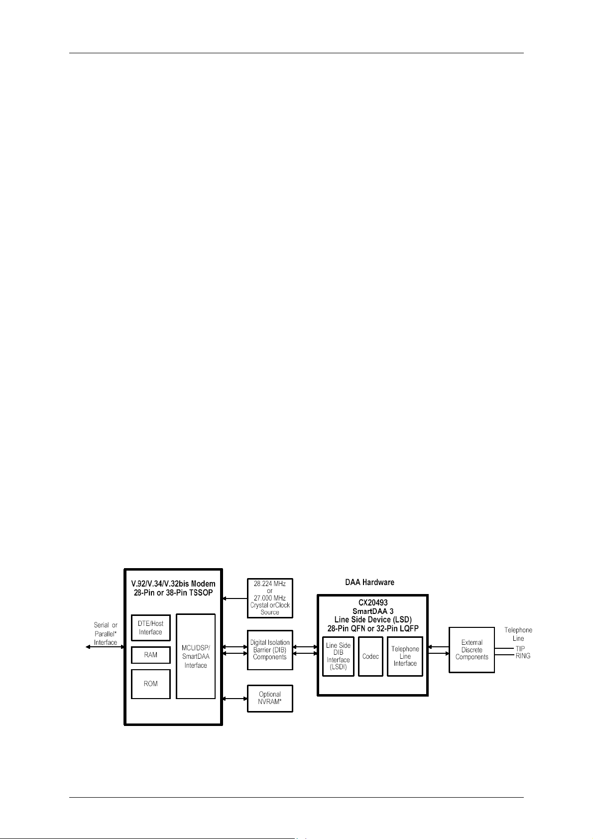
The SmartDAA system-powered DAA operates reliably without drawing power from the line,
unlike line-powered DAAs which operate poorly when line current is insufficient due to long
lines or poor line conditions. Enhanced features, such as monitoring of local extension status
without going off-hook, are also supported.
CX86500
Doc. No. DG_2094E Altec Electronic AG Seite 5 / 30
Page 6

AL2094S Designers Guide
1.2 FEATURES
1.2.1 General Modem Features
• Data modem
- QuickConnect and Modem-on-hold functions
- ITU-T V.92 , V.34 , V.32bis, V.32,
- V.22 bis, V.22, V.23, and V.21; Bell 212A and Bell 103
- V.250 and V.251 commands
• V.22 bis fast connect
• Data compression and error correction
- V.44 data compression
- V.42 bis and MNP 5 data compression
- V.42 LAPM and MNP 2-4 error correction
• Hardware-based modem controller
• Hardware-based digital signal processor (DSP)
• Worldwide operation
- Complies to TBR21 and other country requirements
- Caller ID detection for many countries
- Call progress, blacklisting
- Internal ROM includes default values for 29 countries
- Additional modified country profiles can be stored in internal SRAM
• Caller ID detect
- On-hook Caller ID detection
- Off-hook Call Waiting Caller ID detection during data mode in V.90, V.34,
V.32bis, and V.32
• Distinctive ring detect
• Built-in DTE interface
• Serial ITU-T V.24 (EIA/TIA-232-E) logical interface up to 115.2 kbps
• Direct mode (serial DTE interface)
• Flow control and speed buffering
• Automatic format/speed sensing
• Serial async/sync data
• +3.3V operation with +5V tolerant digital inputs
• Typical power use
- 220 mW (Normal Mode)
- 56 mW (Sleep Mode)
1.2.2 SmartDAA Features
• System side powered DAA operates under poor line current supply conditions
• Modem Wake-on-Ring
• Ring detection
• Line polarity reversal detection
• Line current loss detection
• Pulse dialing
• Line-in-use detection during on-hook operation
• Remote hang-up detection for efficient call termination
• Extension pickup detection
• Call waiting detection
• Digital PBX line protection
• Meets worldwide DC VI masks requirements
Doc. No. DG_2094E Altec Electronic AG Seite 6 / 30
Page 7

AL2094S Designers Guide
1.3 TECHNICAL OVERVIEW
1.3.1 General Description
Modem operation, including dialing, call progress, telephone line interface, telephone
handset interface, and host DTE interface functions are supported and controlled through the
V.250, V.251, and V.253-compatible command set.
1.3.2 MCU Firmware
MCU firmware performs processing of general modem control, command sets, data modem,
error correction and data compression (ECC), fax class 1, fax class 1.0, voice/audio/TAM,
worldwide, V.80, and serial DTE host interface functions according to modem models (Table
1-1).
1.3.3 Operating Modes
In V.90 data modem mode (V.92 models), the modem can receive data from a digital source
using a V.92-compatible central site modem at line speeds up to 56 kbps. Asymmetrical data
transmission supports sending data at line speeds up to V.34 rates. This mode can fallback
to full-duplex V.34 mode and to lower rates as dictated by line conditions.
The following modes are also supported in V.92 models:
• QuickConnect which allows quicker subsequent connection to a server using stored line
parameters obtained during the initial connection. The server must support quick connect
profiles.
• Modem-on-Hold which allows detection and reporting of incoming phone calls on the
PSTN with enabled Call Waiting. If the incoming call is accepted by the user, the user has
a pre-defined amount of time of holding the data connection for a brief conversation. The
data connection resumes upon incoming call termination. The server must support
Modem-on-Hold functionality.
In V.34 data modem mode (V.90+ and V.34 models), the modem can operate in 2-wire, fullduplex, asynchronous modes at line rates up to 33.6 kbps. Data modem modes perform
complete handshake and data rate negotiations. Using V.34 modulation to optimize modem
configuration for line conditions, the modem can connect at the highest data rate that the
channel can support from 33600 bps down to 2400 bps with automatic fallback. Automode
operation in V.34 is provided in accordance with PN3320 and in V.32 bis in accordance with
PN2330. All tone and pattern detection functions required by
the applicable ITU or Bell standards are supported.
In V.32 bis data modem mode, the modem can operate at line speeds up to 14.4 kbps.
In V.22 bis fast connect data mode, the modem can connect at 2400 bps with a very short
training time, which is very efficient for small data transfers.
1.3.4 V.44 Data Compression
V.44 provides more efficient data compression than V.42 bis that significantly decreases the
download time for the types of files associated with Internet use. This significant
improvement is most noticeable when browsing and searching the web since HTML text files
are highly compressible. (The improved performance amount varies both with the actual
format and with the content of individual pages and files.)
Doc. No. DG_2094E Altec Electronic AG Seite 7 / 30
Page 8
AL2094S Designers Guide
1.3.5 Synchronous Access Mode (SAM) - Video Conferencing
V.80 Synchronous Access Mode between the modem and the host/DTE is provided for hostcontrolled communication protocols, e.g., H.324 video conferencing applications. Voice-callfirst (VCF) before switching to a videophone call is also supported.
1.3.6 Worldwide Operation
The modem operates in TBR21-compliant and other countries. Country-dependent modem
parameters for functions such as dialing, carrier transmit level, calling tone, call progress
tone detection, answer tone detection, blacklisting, caller ID, and relay control are
programmable.
SmartDAA technology allows a single PCB design and single BOM to be homologated
worldwide. Advanced features such as extension pickup detection, remote hang-up
detection, line-in-use detection, and digital PBX detection are supported. Country code IDs
are defined by ITU-T T.35.
Internal ROM includes default profiles for 29 countries including TBR21-compliant profiles.
Additional country profiles can be stored in internal SRAM (request additional country
profiles from a Conexant Sales Office). Duplicate country profiles stored in internal SRAM
will override the profiles in internal RAM firmware. The default countries supported are listed
in Table 1-2.
Doc. No. DG_2094E Altec Electronic AG Seite 8 / 30
Page 9
AL2094S Designers Guide
22.. TTEECCHHNNIICCAALL SSPPEECCIIFFIICCAATTIIOONNSS
2.1 Serial DTE Interface Operation
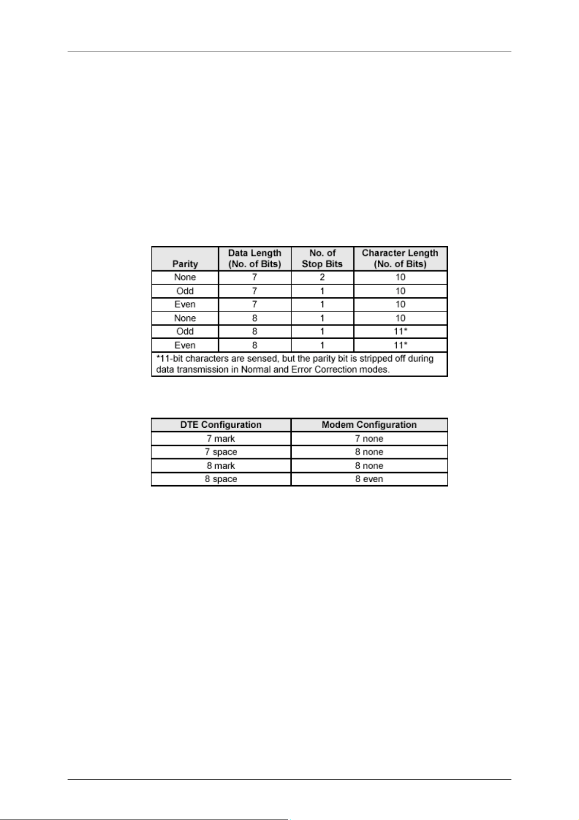
2.1.1 Automatic Speed/Format Sensing
Command Mode and Data Modem Mode. The modem can automatically determine the
speed and format of the data sent from the DTE. The modem can sense speeds of 300, 600,
1200, 2400, 4800, 7200, 9600, 12000, 14400, 16800, 19200, 21600, 24000, 26400, 28800,
38400, 57600, and 115200 bps and the following data formats:
The modem can speed sense data with mark or space parity and configures itself as follows:
Fax Modem Mode. In V.17 fax mode, the modem can sense speeds up to 115.2 kbps.
2.2 Establishing Data Modem Connections
2.2.1 Telephone Number Directory
The modem supports four telephone number entries in a directory that can be saved in a
serial NVRAM. Each telephone number can be up to 32 characters (including the command
line terminating carriage return) in length. A telephone number can be saved using the
&Zn=x command, and a saved telephone number can be dialed using the DS=n command.
2.2.2 Dialing
DTMF Dialing. DTMF dialing using DTMF tone pairs is supported in accordance with ITU-T
Q.23. The transmit tone level complies with Bell Publication 47001.
Pulse Dialing. Pulse dialing is supported in accordance with EIA/TIA-496-A.
Blind Dialing. The modem can blind dial in the absence of a dial tone if enabled by the X0,
X1, or X3 command.
Doc. No. DG_2094E Altec Electronic AG Seite 9 / 30
Page 10
AL2094S Designers Guide
2.2.3 Modem Handshaking Protocol
If a tone is not detected within the time specified in the S7 register after the last digit is
dialed, the modem aborts the call attempt.
2.2.4 Call Progress Tone Detection
Ringback, equipment busy, congested tone, warble tone, and progress tones can be
detected in accordance with the applicable standard.
2.2.5 Answer Tone Detection
Answer tone can be detected over the frequency range of 2100 ± 40 Hz in ITU-T modes and
2225 ± 40 Hz in Bell modes.
2.2.6 Ring Detection
A ring signal can be detected from a TTL-compatible 15.3 Hz to 68 Hz square wave input.
2.2.7 Billing Protection
When the modem goes off-hook to answer an incoming call, both transmission and reception
of data are prevented for 2 seconds (data modem) or 4 seconds (fax adaptive answer) to
allow transmission of the billing tone signal.
2.2.8 Connection Speeds
The modem functions as a data modem when the +FCLASS=0 command is active. Line
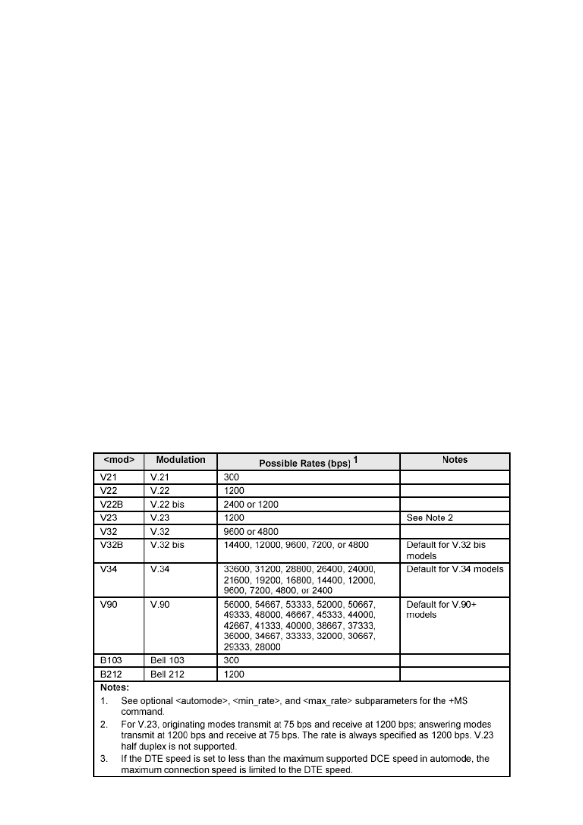
connection can be selected using the +MS command. The +MS command selects
modulation, enables/disables automode, and selects minimum and maximum line speeds
(Table 2-1).
2.2.9 Automode
Automode detection can be enabled by the +MS command to allow the modem to connect to
a remote modem in accordance with draft PN-3320 for V.34 (Table 2-1).
Table 2-1. +MS Command Automode Connectivity
Doc. No. DG_2094E Altec Electronic AG Seite 10 / 30
Page 11

AL2094S Designers Guide
2.3 Data Mode
Data mode exists when a telephone line connection has been established between modems
and all handshaking has been completed.
2.3.1 Speed Buffering (Normal Mode)
Speed buffering allows a DTE to send data to, and receive data from, a modem at a speed
different than the line speed. The modem supports speed buffering at all line speeds.
2.3.2 Flow Control
DTE-to-Modem Flow Control. If the modem-to-line speed is less than the DTE-tomodem
speed, the modem supports XOFF/XON or RTS/CTS flow control with the DTE to ensure
data integrity.
2.3.3 Escape Sequence Detection
The +++ escape sequence can be used to return control to the command mode from the
data mode. Escape sequence detection is disabled by an S2 Register value greater than
127.
2.3.4 BREAK Detection
The modem can detect a BREAK signal from either the DTE or the remote modem. The \Kn
command determines the modem response to a received BREAK signal.
2.3.5 Telephone Line Monitoring
GSTN Cleardown (V.90, V.34, V.32 bis, V.32). Upon receiving GSTN Cleardown from the
remote modem in a non-error correcting mode, the modem cleanly terminates the call.
Loss of Carrier (V.22 bis and Below). If carrier is lost for a time greater than specified by
the S10 register, the modem disconnects (except MNP 10).
2.3.6 Fall Forward/Fallback (V.90/V.34/V.32 bis/V.32)
During initial handshake, the modem will fallback to the optimal line connection within
V.90/V.34/V.32 bis/V.32 mode depending upon signal quality if automode is enabled by the
+MS or N1 command.
When connected in V.90/V.34/V.32 bis/V.32 mode, the modem will fall forward or fallback to
the optimal line speed within the current modulation depending upon signal quality if fall
forward/fallback is enabled by the %E2 command.
2.3.7 Retrain
The modem may lose synchronization with the received line signal under poor or changing
line conditions. If this occurs, retraining may be initiated to attempt recovery depending on
the type of connection. The modem initiates a retrain if line quality becomes unacceptable if
enabled by the %E
command. The modem continues to retrain until an acceptable connection is achieved, or
until 30 seconds elapse resulting in line disconnect.
2.3.8 Programmable Inactivity Timer
The modem disconnects from the line if data is not sent or received for a specified length of
time. In normal or error-correction mode, this inactivity timer is reset when data is received
from either the DTE or from the line. This timer can be set to a value between 0 and 255
seconds by using register S30. A value of 0 disables the inactivity timer.
2.3.9 DTE Signal Monitoring (Serial DTE Interface Only)
DTR#. When DTR# is asserted, the modem responds in accordance with the &Dn and &Qn
commands.
RTS#. RTS# is used for flow control if enabled by the &K command in normal or error
correction mode.
Doc. No. DG_2094E Altec Electronic AG Seite 11 / 30
Page 12

AL2094S Designers Guide
2.4 Modem-on-Hold
The Modem-on-Hold (MOH) function (V.92 models only) enables the modem to place a data
call to the Internet on hold while using the same line to accept an incoming or place an
outgoing voice call. This feature is available only with a connection to a server supporting
MOH. MOH can be executed through either of two methods:
• One method is to enable MOH through the +PMH command. With Call Waiting
Detection (+PCW command) enabled, an incoming call can be detected while online.
Using a string of commands, the modem negotiates with the server to place the data
connection on hold while the line is released so that it can be used to conduct a voice
call. Once the voice call is completed, the modem can quickly renegotiate with the
server back to the original data call.
• An alternative method is to use communications software that makes use of the
Conexant Modem-on-Hold drivers. Using this method, the software can detect an
incoming call, place the data connection on hold, and switch back to a data connection.
2.5 Error Correction and Data Compression
2.5.1 V.42 Error Correction
V.42 supports two methods of error correction: LAPM and, as a fallback, MNP 4. The
modem provides a detection and negotiation technique for determining and establishing the
best method of error correction between two modems.
2.5.2 MNP 2-4 Error Correction
MNP 2-4 is a data link protocol that uses error correction algorithms to ensure data integrity.
Supporting stream mode, the modem sends data frames in varying lengths depending on the
amount of time between characters coming from the DTE.
2.5.3 V.44 Data Compression
V.44 data compression encodes pages and files associated with Web pages more efficiently
than V.42 bis. These files include WEB pages, graphics and image files, and document files.
V.44 can provide an effective data throughput rate up to DTE rate for a 56-kbps connection.
The improved performance amount varies both with the actual format and with the content of
individual pages and files.
2.5.4 V.42 bis Data Compression
V.42 bis data compression mode, enabled by the %Cn command or S46 register, operates
when a LAPM or MNP 10 connection is established. The V.42 bis data compression employs
a “string learning” algorithm in which a string of characters from the DTE is encoded as a
fixed length codeword. Two 2-KB dictionaries are used to store the strings. These
dictionaries are dynamically updated during normal operation.
2.5.5 MNP 5 Data Compression
MNP 5 data compression mode, enabled by the %Cn command, operates during an MNP
connection.
In MNP 5, the modem increases its throughput by compressing data into tokens before
transmitting it to the remote modem, and by decompressing encoded received data before
sending it to the DTE.
2.6 MNP 10 Data Throughput Enhancement
MNP 10 protocol and MNP Extended Services enhance performance under adverse channel
conditions such as those found in rural, long distance, or cellular environments. An MNP 10
connection is established when an MNP 2-4 connection is negotiated with a remote modem
supporting MNP 10.
MNP Extended Services. The modem can quickly switch to MNP 10 operation when the
remote modem supports MNP 10 and both modems are configured to operate in V.42.
V.42 bis/MNP 5 Support. V.42 bis/MNP 10 can operate with V.42 bis or MNP 5 data
compression.
Doc. No. DG_2094E Altec Electronic AG Seite 12 / 30
Page 13

AL2094S Designers Guide
2.7 Telephony Extensions
The following telephony extension features are supported and can be typically be
implemented in designs for set-top box applications and TAM software applications to
enhance end-user experience:
• Line In Use detection
• Extension Pickup detection
• Remote Hang-up detection
2.7.1 Line In Use Detection
The Line In Use Detection feature can stop the modem from disturbing the phone line when
the line is already being used. When an automated system tries to dial using ATDT and the
phone line is in use, the modem will not go off hook and will respond with the message “LINE
IN USE”.
2.7.2 Extension Pickup Detection
The Extension Pickup Detection feature (also commonly referred as PPD or Parallel phone
detection) allows the modem to detect when another telephony device (i.e., fax machine,
phone, satellite/cable box) is attempting to use the phone line. This feature can be used to
quickly drop a modem connection in the event when a user picks up a extension phone line.
For example, this feature allows set top boxes with an integrated SmartV.XX modem to give
normal voice users the highest priority over the telephone line. This feature can also be used
in Telephone Answering Machine applications (TAM). Its main use would be to stop the TAM
operation when a phone is picked up.
2.7.3 Remote Hangup Detection
The Remote Hangup Detection feature will cause the modem go back onhook during a data
connection when the remote modem is disconnected for abnormal termination reasons
(remote phone line unplugged, remote server/modem shutdown. For Voice applications, this
method can be used in addition to silence detection to determine when a remote caller has
hung up to terminate a voice recording.
2.8 Caller ID
Both Type I Caller ID (On-Hook Caller ID) and Type II Caller ID (Call Waiting Caller ID) are
supported for U.S. and many other countries (see Section 2.11). Both types of Caller ID are
enabled/disabled using the +VCID command. Call Waiting Tone detection must be enabled
using the +PCW command to detect and decode Call Waiting Caller ID.
When enabled, caller ID information (date, time, caller code, and name) can be passed to
the DTE in formatted or unformatted form. Inquiry support allows the current caller ID mode
and mode capabilities of the modem to be retrieved from the modem. Type II Caller ID (Call
Waiting Caller ID) detection operates only during data mode in V.90, V.34, V.32bis, or V.32.
2.9 Worldwide Country Support
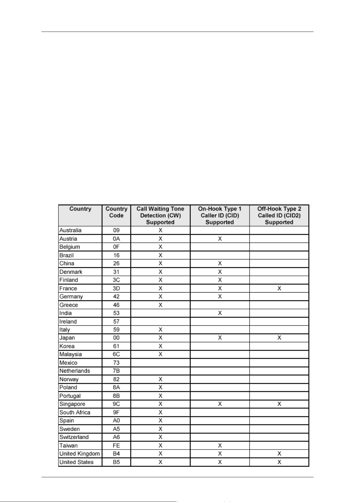
Internal modem firmware supports 29 country profiles (see Section 1.3.2). These country
profiles include the following country-dependent parameters:
• Dial tone detection levels and frequency ranges.
• DTMF dialing parameters: Transmit output level, DTMF signal duration, and DTMF
interdigit interval.
• Pulse dialing parameters: Make/break times, set/clear times, and dial codes are
programmable
• Ring detection frequency range.
• Type I and Type II Caller ID are supported for many countries. Consult firmware release
notes for a list of the supported countries and the criteria for additional country support.
• Blind dialing enabled/disable.
• Carrier transmit level (through S91 for data and S92 for fax). The maximum, minimum,
and default values can be defined to match specific country and DAA requirements.
Doc. No. DG_2094E Altec Electronic AG Seite 13 / 30
Page 14

AL2094S Designers Guide
• Calling tone is generated in accordance with V.25. Calling tone may be toggled
(enabled/disabled) by inclusion of a “^” character in a dial string. It may also be
disabled.
• Frequency and cadence of tones for busy, ringback, congested, warble, dial tone 1, and
dial tone 2.
• Answer tone detection period.
• Blacklist parameters. The modem can operate in accordance with requirements of
individual countries to prevent misuse of the network by limiting repeated calls to the
same number when previous call attempts have failed. Call failure can be detected for
reasons such as no dial tone, number busy, no answer, no ringback detected, voice
(rather than modem) detected, and key abort (dial attempt aborted by user). Actions
resulting from such failures can include specification of minimum inter-call delay,
extended delay between calls, and maximum numbers of retries before the number is
permanently forbidden ("blacklisted").
2.10 Diagnostics
Commanded Tests
Diagnostics are performed in response to &T commands.
Analog Loopback (&T1 Command). Data from the local DTE is sent to the modem, which
loops the data back to the local DTE.
2.11 Low Power Sleep Mode
Sleep Mode Entry. The modem enters the low power sleep mode when no line connection
exists and no host activity occurs for the period of time specified in the S24 register. All
modem circuits are turned off except the internal clock circuitry in order to consume reduced
power while being able to immediately wake up and resume normal operation.
Wake-up. Wake-up occurs when a ring is detected on the telephone line or the DTE sends a
character to the modem.
Doc. No. DG_2094E Altec Electronic AG Seite 14 / 30
Page 15

AL2094S Designers Guide
33.. HHAARRDDWWAARREE IINNTTEERRFFAACCEE
3.1 AL2094S Modem Hardware Pins and Signals
3.1.1 Phone Line Interface
The phone-line interface signals are:
• TIP
• RING
3.1.2 Call Progress Speaker Interface
The call progress speaker interface signal is:
• Digital speaker output (DSPKOUT); output
DSPKOUT is a square wave output in Data/Fax mode used for call progress or carrier
monitoring. This output can be optionally connected to a low-cost on-board speaker, e.g.,
a sounducer, or to an analog speaker circuit.
3.1.3 Serial DTE Interface and Indicator Outputs
The supported DTE interface signals are:
• Serial Transmit Data input (TXD#)
• Serial Receive Data output line (RXD#)
• Clear to Send output (CTS#)
• Received Line Signal Detector (DCD#)
• Ring Indicator (RI#)
• Data Terminal Ready control input (DTR#)
• Request to Send control input (RTS#)
Additional clock signals provided for synchronous mode are:
• Receive Data Clock (RXCLK#)
• Transmit Data Clock (TXCLK#)
3.1.4 External Reset Input
The supported reset input interface signals are:
• External Reset Input (EXTRESET#)
3.1.5 AL2094S Modem Pin Assignments and Signal Definitions
AL2094S Modem DIL-40 hardware interface signals are shown by major interface in Figure
3-1, are shown by pin number in Figure 3-2, and are listed by pin number in Table 1-1.
AL20XX Modem hardware interface signals are defined in Table 3-2.
I/O types are defined in Table 3-3.
DC electrical characteristics are listed in Table 3-4.
Doc. No. DG_2094E Altec Electronic AG Seite 15 / 30
Page 16

IGURE 3-1. AL2094S MODEM HARDWARE SIGNALS
F
Table 3-1. AL2094S Modem DIL-40 Pin Signals
Pin No NAME Pin No NAME
1 GND 40 RXD
2 GND 39 TXD
3 VCC1 38 DTR
4 VCC2 37 DCD
5 EXTRESET 36 DSR/DCD
6 NC 35 CTS
7 DSPKOUT 34 RTS
8 TDCLK 33 RI
9 RDCLK 32 NC
10 …18 No pin 31… 23 No pin
19 NC 22 NC
20 RING 21 TIP
AL2094S Designers Guide
19
20
1
2
3
4
5
6
7
8
9
GND
GND
VCC1
VCC2
RESET
NC
SPKOUT
TDCLK
RDCLK
NC
RING
RXD
TXD
DTR
DCD
DCD
CTS
RTS
RI
NC
NC
TIP
40
39
38
37
36
35
34
33
32
22
21
Doc. No. DG_2094E Altec Electronic AG Seite 16 / 30
Page 17

AL2094S Designers Guide
Table 3-2. Signal Descriptions
Label Pin I/O I/O Type Signal Name/Description
VCC 3,4 P PWR Digital Supply Voltage. Connect to VCC (+3.3V, filtered).
GND 1,2 G GND Digital Ground. Connect to digital ground (GND).
Reset. . Open collector input/output. Drive only with opencollector circuit.
The active low RESET# input resets the Modem logic and
clears the internal SRAM. RESET# low holds the modem in
RESET 5 I IC/OC
SPKOUT 7 O It/Ot2
the reset state; RESET# going high releases the modem from
the reset state. RESET# is connected to a built-in reset circuit
on the Socket Modem.
Connect to Ground through an 1nF capacitor to ensure good
ESD immunity and to comply with ESD tests according to EN
61000-4-2.
Modem Speaker Digital Output. The DSPKOUT digital
output reflects the received analog input signal digitized to
TTL high or low level by an internal comparator.
TIP 21 P Passive
RING 20 P Passive
TXD 39 I It/Ot2
RXD 40 O It/Ot2
CTS 35 O Ith/Ot8
DCD 37 O Ith/Ot8
TIP Signal from Telco/PTT
RING Signal from Telco/PTT
Transmitted Data (EIA BA/ITU-T CT103). The DTE uses the
TXD# line to send data to the modem for transmission over
the telephone line or to transmit commands to the modem.
Received Data (EIA BB/ITU-T CT104). The modem uses the
RXD# line to send data received from the telephone line to the
DTE and to send modem responses to the DTE. During
command mode, RXD# data represents the modem
responses to the DTE.
Clear To Send (EIA CB/ITU-T CT106). CTS# output ON (low)
indicates that the modem is ready to accept data from the
DTE. In asynchronous operation, in error correction or normal
mode, CTS# is always ON (low) unless RTS/CTS flow control
is selected by the &Kn command. In synchronous operation,
the modem also holds CTS# ON during asynchronous
command state. The modem turns CTS# OFF immediately
upon going off-hook and holds CTS# OFF until both DSR#
and DCD# are ON and the modem is ready to transmit and
receive synchronous data. The modem can also be
commanded by the &Rn command to turn CTS# ON in
response to an RTS# OFF-to-ON transition.
Received Line Signal Detector (EIA CF/ITU-T CT109).
When AT&C0 command is not in effect, DCD# output is ON
when a carrier is detected on the telephone line or OFF when
carrier is not detected.
DSR 36 O Ith/Ot8
RI 33 O Ith/Ot8
DTR 38 I It
Data set ready. This signal is not supported. This output is
hardwired to the DCD signal. Same as pin 37.
Ring Indicator (EIA CE/ITU-T CT125). RI# output ON (low)
indicates the presence of an ON segment of a ring signal on
the telephone line.
Data Terminal Ready (EIA CD/ITU-T CT108). The DTR#
input is turned ON (low) by the DTE when the DTE is ready to
transmit or receive data. DTR# ON prepares the modem to be
connected to the telephone line, and maintains the connection
established by the DTE (manual answering) or internally
(automatic answering). DTR# OFF places the modem in the
disconnect state under control of the &Dn and &Qn
commands.
Doc. No. DG_2094E Altec Electronic AG Seite 17 / 30
Page 18

AL2094S Designers Guide
Table 3-3. Signal Descriptions (Cont'd)
Label Pin I/O I/O Type Signal Name/Description
Request To Send (EIA CA/ITU-T CT105). RTS# input ON
(low) indicates that the DTE is ready to send data to the
modem. In the command state, the modem ignores RTS#.
In asynchronous operation, the modem ignores RTS# unless
RTS 34 I Ithpu
RXCLK 9 O Itpu/Ot2
TXCLK 8 O Itpu/Ot2
Table 3-4. AL2094S Modem I/O Type Definitions
I/O Type Description
It/Ot2 Digital input, +5V tolerant/ Digital output, 2 mA, ZINT = 120 Ω
Itpu/Ot2 Digital input, +5V tolerant, 75k Ω pull up/ Digital output, 2 mA, ZINT = 120 Ω
Ith/Ot8 Digital input, +5V tolerant, hysteresis/Digital output, 8 mA, ZINT = 50 Ω
It Digital input, +5V tolerant
Ithpu Digital input, +5V tolerant, hysteresis, 75k Ω pull up
IC/OC Open collector input/output, internal 10k pull-up
PWR VCC Power
GND Ground
NOTES:
I/O Type corresponds to the device Pad Type. The I/O column in signal interface tables refers to
signal I/O direction used in the application.
Table 3-5. AL2094S Modem DC Electrical Characteristics
Parameter Symbol Min Typ Max Units
Input Voltage Low VIL
+5V tolerant 0 - 0.8 V
+5V tolerant hysteresis 0 - 0.3 * VGG V
Input Voltage High VIH
+5V tolerant 2 - 5.25 V
+5V tolerant hysteresis 0.7 * VDD - 5.25 V
Input Hysteresis VH
+3V hysteresis 0.5 - V
+5V tolerant,hysteresis 0.3 - V
Output Voltage Low VOL
ZINT = 120 Ω 0 - 0.4 V IOL = 2 mA
ZINT = 50 Ω
Output Voltage High VOH
ZINT = 120 Ω 2.4 - VDD V IOL = - 2 mA
ZINT = 50 Ω
Pull-Up Resistance Rpu 50 - 200 kΩ
Pull-Down Resistance Rpd 50 - 200 kΩ
Test Conditions unless otherwise stated: VDD = +3.3 ± 0.3 VDC; TA = 0°C to 70°C; external load = 50 pF.
Doc. No. DG_2094E Altec Electronic AG Seite 18 / 30
RTS/CTS flow control is selected by the &Kn command. In
synchronous on-line operation, the modem can be
commanded by the &Rn command to ignore RTS# or to
respond to RTS# by turning on CTS# after the delay specified
by Register S26.
Receive Data Clock. A synchronous Receive Data Clock
(RXCLK) is output in synchronous modes. The RXCLK
frequency is the data rate (±0.01%) with a duty cycle of
50±1%. Leave open if not used.
Transmit Data Clock. A synchronous Transmit Data Clock
(TXCLK) is output in synchronous modes. The TXCLK
frequency is the data rate (±0.01%) with a duty cycle of
50±1%. Leave open if not used.
Test
Conditions
0 - 0.4 V IOL = 8 mA
2.4 - VDD V IOL = - 8 mA
Page 19

AL2094S Designers Guide
3.3 Electrical and Environmental Specifications
3.3.1 Operating Conditions, Maximum Ratings, Power Requirements.
The operating conditions are specified in Table 3-9.
The absolute maximum ratings are listed in Table 3-10.
The current and power requirements are listed in Table 3-11.
Table 3-9. Operating Conditions
Parameter Symbol Limits Units
Supply Voltage VDD + 3.0 to +3.6 VDC
Operating Ambient Temperature TA 0 to + 70 °C
Table 3-10. Absolute Maximum Ratings
Parameter Symbol Limits Units
Supply Voltage VDD -0.5 to + 4.0 VDC
Input Voltage VIN -0.5 to (VGG +0.5)* VDC
Storage Temperature Range T
Analog Inputs VIN -0.3 to (VAA + 0.5) VDC
Voltage Applied to Outputs in
High Impedance (Off) State
DC Input Clamp Current IIK ±20 mA
DC Output Clamp Current IOK ±20 mA
Static Discharge Voltage (25°C) V
Latch-up Current (25°C) I
* VGG = +3.3V ± 0.3V or +5V ± 5%.
Handling CMOS Devices
The device contains circuitry to protect the inputs against damage due to high static
voltages. However, it is advised that normal precautions be taken to avoid application of
any voltage higher than maximum rated voltage.
An unterminated input can acquire unpredictable voltages through coupling with stray
capacitance and internal cross talk. Both power dissipation and device noise immunity
degrades. Therefore, all inputs should be connected to an appropriate supply voltage.
Input signals should never exceed the voltage range from -0.5V to VGG + 0.5V. This
prevents forward biasing the input protection diodes and possibly entering a latch up
mode due to high current transients.
Table 3-11. Current and Power Requirements
Mode
Normal Mode: Off-hook, normal data connection 66 73 220 240
Normal Mode: On-hook, idle, waiting for ring 61 67 200 220
Sleep Mode 17 19 56 63
Notes:
1. Operating voltage: VDD = +3.3V ± 0.3V.
2. Test conditions: VDD = +3.3V for typical values; VDD = +3.6V for maximum values.
3. Input Ripple ≤ 0.1 Vpeak-peak.
4. f = Internal frequency.
5. Maximum current computed from Ityp: Imax = Ityp * 1.1.
6. Typical power (Ptyp) computed from Ityp: Ptyp = Ityp * 3.3V; Maximum power (Pmax) computed from Imax:
Pmax = Imax * 3.6V.
-55 to + 125 °C
STG
VHZ -0.5 to (VGG + 0.5)* VDC
±2500 VDC
ESD
±400 mA
TRIG
Typical
Current
(Ityp)
(mA)
Maximum
Current
(Imax)
(mA)
Typical
Power
(Ptyp)
(mW)
Maximum
Power
(Pmax)
(mW)
Doc. No. DG_2094E Altec Electronic AG Seite 19 / 30
Page 20

AL2094S Designers Guide
3.3.2 Interface and Timing Waveforms
3.3.2.1 Serial DTE Interface
The serial DTE interface waveforms for 4800 and 9600 bps are illustrated in Figure 3-5.
F
IGURE 3-5. WAVEFORMS - SERIAL DTE INTERFACE
Doc. No. DG_2094E Altec Electronic AG Seite 20 / 30
Page 21

AL2094S Designers Guide
3.4 DAA Interface
The Socket Modem is configured to be an on-board DAA (World Class DAA).
Provide TIP and RING signals from the telco jack to pins 20 and 21 of the Socket Modem.
Only EMI suppression and surge protection components may be used. If other components
are used, the PTT certification for these Socket Modems will no longer apply, and
recertification will be required.
The recommended telco interface for U.S. Socket Modems is shown in Figure 3-3.
The recommended telco interface for World Class Socket Modems is shown in Figure 3-4.
TIP and RING signal traces are to be no closer than 2.5mm (0.1") from any other traces for
European applications. 2.5mm spacing must be used if the host board is to support both
U.S. and European Socket Modems.
C1
1000PF
X2/Y3
R1
0R
F1
F1250T
P2
1
2
L1
1
4
8
5 RV1
P3100SC
1
NC
2
OT
3
T
4
R
5
OR
6
NC
SOCKET MODEM
R2
0R
C2
1000PF
X2/Y3
RJ11
Note: Meets FCC Part 68 Type A and Type B Surge Requirements (Type A Non-Operational)
IGURE 3-3. RECOMMENDED TELEPHONE LINE INTERFACE FOR U.S. SOCKET MODEM
F
P1
Doc. No. DG_2094E Altec Electronic AG Seite 21 / 30
Page 22

(
SOCKET MODEM
P2
AL2094S Designers Guide
C1
1000PF
X2/Y3
R1
0R
1
2
L1
1
4
8
5
R2
0R
F1
TS250-130
RV1
TVB270SC
C2
1000PF
X2/Y3
P1
1
NC
2
OT
3
T
4
R
5
OR
6
NC
RJ11
Note: Meets ITU-T K.21 Surge Requirements
F
IGURE 3-4. RECOMMENDED TELEPHONE LINE INTERFACE FOR WORLD CLASS SOCKET MODEM.
The common mode choke L1 is optional in both Figures 3.3 and 3.4 and it’s need depends on the
characteristics of the target hardware. The need for this choke must be evaluated at EMV
measurement
conducted emission) of the final product. If not used populate R1, R2.
Table 3-7. DAA Part List
REF
TYPE
Manufacturer
PART No
L1
Common Mode Coke
Epcos
Microspire
B82790-C0475-N265
ESC-X1-M47-1S
C1, C2
High Voltage Capacitor / MLCC
X2 / Y3 Types
Johansson
Novacap
Syfer
302R29W102KV3E
LS1808N102K302
1808JA250102KCT
F1
RV1
Fuse: U.S. Models
Europe Models
Thyristor Surge Protectors:
U.S. Models
Europe Models
Littlefuse
Raychem
Teccor
Raychem
F1250T
TS250-130
P3100SC
TVB270SC
Doc. No. DG_2094E Altec Electronic AG Seite 22 / 30
Page 23

AL2094S Designers Guide
44..
DDEESSIIGGNN CCOONNSSIIDDEERRAATTIIOONNSS
Good engineering practices must be adhered to when designing a printed circuit board
(PCB) containing the Socket Modem module. Suppression of noise is essential to the proper
operation and performance of the modem itself and for surrounding equipment.
Two aspects of noise in an OEM board design containing the Socket Modem module must
be considered: on-board/off-board generated noise that can affect analog signal levels and
analog-to-digital conversion (ADC)/digital-to-analog conversion (DAC), and on-board
generated noise that can radiate off-board. Both on-board and off-board generated noise
that is coupled on-board can affect interfacing signal levels and quality, especially in low
level analog signals. Of particular concern is noise in frequency ranges affecting modem
performance.
On-board generated electromagnetic interference (EMI) noise that can be radiated or
conducted off-board is a separate, but equally important, concern. This noise can affect the
operation of surrounding equipment. Most local governing agencies have stringent
certification requirements that must be met for use in specific environments.
Proper PC board layout (component placement, signal routing, trace thickness and
geometry, etc.), component selection (composition, value, and tolerance), interface
connections, and shielding are required for the board design to achieve desired modem
performance and to attain EMI certification.
The aspects of proper engineering practices are beyond the scope of this designer's guide.
The designer should consult noise suppression techniques described in technical
publications and journals, electronics and electrical engineering text books, and component
supplier application notes. Seminars addressing noise suppression techniques are often
offered by technical and professional associations as well as component suppliers.
4.1 PC Board Layout Guidelines
4.1.1 General
1. In a 2-layer design, provide an adequate ground grid in all unused space around and
under components (judiciously near analog components) on both sides of the board,
and connect in such a manner as to avoid small islands. A grid is preferred over a plane
to improve solderability. Typically, the grid is composed of 0.012 in. traces and 0.012 in.
spaces on a 0.025 in. grid. Connect each grid to other grids on the same side at several
points and to grids on the opposite side through the board at several points. Connect
Socket Modem DGND and AGND pins to the ground grid.
2. In a 4-layer design, provide an adequate ground plane covering the entire board.
Socket Modem DGND and AGND pins are tied together on the Socket Modem.
3. As a general rule, route digital signals on the component side of the PCB and the
analog signals on the solder side. The sides may be reversed to match particular OEM
requirements. Route the digital traces perpendicular to the analog traces to minimize
signal cross coupling.
4. Route the modem signals to provide maximum isolation between noise sources and
noise sensitive inputs. When layout requirements necessitate routing these signals
together, they should be separated by neutral signals.
5. All power and ground traces should be at least 0.05 in. wide.
6. TIP and RING signal traces are to be no closer than 2.5mm (0.1") from any other traces
for European applications. 2.5mm spacing must be used if the host board is to support
both U.S. and European Socket Modems.
7. If the Socket Modem is mounted flush with the host PCB, the host PCB should be clear
of all traces directly underneath the Socket Modem oscillator section. It is strongly
suggested that the Socket Modem is mounted at least 0.130 inch above the host board.
(See section 4.4)
Doc. No. DG_2094E Altec Electronic AG Seite 23 / 30
Page 24

AL2094S Designers Guide
4.1.2 Electromagnetic Interference (EMI) Considerations
The following guidelines are offered to specifically help minimize EMI generation. Some of
these guidelines are the same as, or similar to, the general guidelines but are mentioned
again to reinforce their importance.
In order to minimize the contribution of the Socket Modem-based design to EMI, the
designer must understand the major sources of EMI and how to reduce them to acceptable
levels.
1. Keep traces carrying high frequency signals as short as possible.
2. Provide a good ground plane or grid. In some cases, a multilayer board may be
required with full layers for ground and power distribution.
3. Decouple power from ground with decoupling capacitors as close to the Socket
Modem module power pins as possible.
4. Eliminate ground loops, which are unexpected current return paths to the power
source and ground.
5. Decouple the telephone line cables at the telephone line jacks. Typically, use a
combination of series inductors, common mode chokes, and shunt capacitors.
Methods to decouple telephone lines are similar to decoupling power lines, however,
telephone line decoupling may be more difficult and deserves additional attention. A
commonly used design aid is to place footprints for these components and populate
as necessary during performance/EMI testing and certification.
6. Decouple the power cord at the power cord interface with decoupling capacitors.
Methods to decouple power lines are similar to decoupling telephone lines.
7. Locate high frequency circuits in a separate area to minimize capacitive coupling to
other circuits.
8. Locate cables and connectors so as to avoid coupling from high frequency circuits.
10. If a mulilayer board design is used, make no cuts in the ground or power planes and
be sure the ground plane covers all traces.
11. Minimize the number of through-hole connections on traces carrying high frequency
signals.
12. Avoid right angle turns on high frequency traces. Forty-five degree corners are good,
however, radius turns are better
13. On 2-layer boards with no ground grid, provide a shadow ground trace on the opposite
side of the board to traces carrying high frequency signals. This will be effective as a
high frequency ground return if it is three times the width of the signal traces.
14. Distribute high frequency signals continuously on a single trace rather than several
traces radiating from one point.
4.2 Other Considerations
The pins of all Socket Modems are grouped according to function. The DAA interface, Host
interface, and LED interface pins are all conveniently arranged, easing the host board layout
design.
Altec Electronic has tested each of the SocketModems for compliance with their respective
country’s PTT requirements and has received PTT certificates that cover, without additional
expense to the user, all applications that use these Socket Modems in their respective
countries. The certificates apply only to designs that route TIP and RING (pins 20 and 21)
directly to the telco jack. Only specified EMI filtering components are allowed on these two
signals as shown in figure 3-3.
Doc. No. DG_2094E Altec Electronic AG Seite 24 / 30
Page 25

AL2094S Designers Guide
4.3 Manufacturing Considerations
The Socket Modem has been designed to be mounted onto the host board in one of two
ways.
The first method consists of soldering a DIP-40 socket to the host board and inserting the
Socket Modem into the socket.
The second way is to solder the Socket Modem directly to the host board. The most efficient
way to do this is through a wave solder process. The recommended hole size for the Socket
Modem pins is 0.036 in. ±0.003 in. in diameter. Spacers can be used to hold the Socket
Modem vertically in place during the wave solder process.
Socket Modems can be put through a water wash process.
Doc. No. DG_2094E Altec Electronic AG Seite 25 / 30
Page 26

AL2094S Designers Guide
∅
55..
PPAACCKKAAGGEE DDIIMMEENNSSIIOONNSS
Package Dimensions are shown in Figure 5-1.
3,5 mm
2,54mm
3,4mm
53 mm
0.5mm
Figure 5-1. AL2094S Socket Modem Physical Dimensions
Bottom View
20.3 mm
1,6mm
4,8 mm
Doc. No. DG_2094E Altec Electronic AG Seite 26 / 30
Page 27

AL2094S Designers Guide
66..
SSOOCCKKEETT MMOODDEEMM AAPPPPRROOVVAALLSS
The Socket Modem module is approved as a host-independent modem card. To maintain
type approvals, permits and/or licenses valid, the guidelines described in this document must
be followed.
6.1 Considerations for Telecom Approvals
The Socket Modem has been assessed and has been found to comply with the relevant
harmonized standards as defined by the European ETSI Directive (ETSI TC-TE).
These standards are: TBR21 / CTR21
6.1.1 PSTN Connection
The Socket Modem can be connected to the Public Switched Telephone Network (PSTN)
either
a) by using a 2-wire flying cable to connect pins 20 and 21 of the card to an RJ-11
connector which can be assembled in a suitable location of the host system enclosure,
OR
b) by providing traces on the host system motherboard for the PSTN connection signals
(TIP and RING) between
If connection option a) is used, the cable and its installation inside the host system must be
in accordance with the guidelines in IEC950/EN60950 (e.g. the insulation material must
withstand electric strength tests as described in section 3.4).
If connection option b) is used, NO additional components except those used for EMI filtering
(specified in figure 3-3) must be connected to the TIP and RING signals. Other components
not intended for use with this design may affect the network access characteristics of the
modem and may therefore invalidate the type approvals, permits and/or licences.
In both cases, for the connection between the host and the PSTN wall connector, a cable
with RJ-11 modular jack and an appropriate national plug must be used. Note that in
Germany, an F-coded connector/plug
for PSTN connection in Germany, the other type is called N-coded).
the card and an RJ-11 connector
must be used (this is one of the two typical plugs used
6.2 Considerations for Electrical Safety
6.2.1 Conditions for Maintaining Safety Compliance (European Countries)
The Socket Modem has been assessed with respect to electrical safety and has been found
to comply with relevant standards as defined by the European Low Voltage Directive
(72/23EEC). The particular standard is EN 60950-1:2001
The card is rated as Class III equipment and it is intended for use in Pollution Degree 2
environments only [see EN60950-1:2001, 2.10.4]. Material Group IIIa or IIIb (Comparative
Tracking Index below 400 according o IEC 112, method A) is assumed for any host system
PCB that has traces and/or circuitry with TNV potential.
It is assumed that the modem card will only be assembled in a host system unit that
complies with IEC60950/EN60950.
Some particular requirements are [see EN60950-1:2001, 2.1.1, 2.2, 2.3, 2.9, 2.10 and
4.7.3.2]:
- the host system must have a compliant fire enclosure (e.g. made of material with
flammability class 94V-1 or better).
- the power supply unit of the host system must have double or reinforced insulation.
Doc. No. DG_2094E Altec Electronic AG Seite 27 / 30
.
Page 28

AL2094S Designers Guide
6.2.2 Power Supply [EN60950-1:2001, 1.6]
Before installing the Socket Modem in a host system, the installer must ensure that the
power drawn by the card, together with the host and any auxiliary cards drawing power from
the host, is within the rating of the host power supply unit.
The Socket Modem's power consumption is typically 0.25 W (+3.3 Vdc).
6.2.3 Clearances, Creepage Distances and Distances through Insulation
[EN60950-1:2001, 2.10.3 and 2.10.4]
This card must be installed such that with the exception of the connections to the host,
clearance and creepage distances shown in the table below are maintained between
a) the TNV3 area of the card (the DAA) and conductive parts of other assemblies inside
the host,
b) if applicable, the PSTN connection traces (TIP and RING) routed through the host
system motherboard and any other conductive area (i.e. traces, through holes, SMD
pads, copper areas, etc.) on that motherboard,
which use or generate a voltage shown in the table below (values only for secondary
circuits):
SELV
a/b RS 232
TNV3
EN60950:2000 Table 2K / 2L
Clearance (mm) Creepage (mm)
Voltage used or
Generated by Host or
Other cards
1.0
2.0
2.5
1.5 (2.4)
2.5 (4.0)
3.2 (5.0)
Up to 125 Vrms or Vdc
Up to 250 Vrms or Vdc
Up to 300 Vrms or Vdc
The larger distances shown in brackets applies for Pollution Degree 3 environments (where
the local environment within the host is subject to conductive pollution or dry non-conductive
pollution, which could become conductive due to expected condensation).
The same clearance and creepage distances also apply between TNV3 areas of the card
and earth connections inside the host system.
Doc. No. DG_2094E Altec Electronic AG Seite 28 / 30
Page 29

AL2094S Designers Guide
Clearance and creepage between primary (mains) and secondary circuits according EN
60950-1:2001, clause 2.10.3.2 table 2H and clause 2.10.4 table 2L.
Minimum distances between primary and secondary circuits (f.g. for mains voltage 230 V
Clearance = 4 mm
Creepage = 5 mm
Failure to maintain these minimum distances would invalidate the approval.
NOTE: For a host or other expansion cards fitted in the host using or generating voltages
greater than 300 V (rms or dc), advice from a competent telecommunications safety
engineer must be obtained.
If these clearance and creepage distances cannot be provided inside the host due to space
limitations, a dielectric material may be used as a physical insulation barrier. The dielectric
material used in this insulation must have a thickness of at least 0.4mm
After installation (or implementation) of the Socket Modem inside a host system, it is
recommended that a competent telecommunications safety engineer inspects the
complete system to ensure that safety compliance is maintained.
(TNV = Telecommunications Network Voltages)
.
AC
):
Doc. No. DG_2094E Altec Electronic AG Seite 29 / 30
Page 30

AL2094S Designers Guide
6.3 Considerations for EMC
6.3.1 EMC Compliance (European Countries)
The Socket Modem has been assessed with respect to emission of and immunity to
electromagnetic disturbances and has been found to comply with the relevant harmonized
standards as defined by the European EMC Directive (89/336/EEC).
These standards are:
• Generic emission standards which refers to
EN 55022:1998 +A1:2000, Class B
• Generic immunity standards which refers to
EN 55024:1998 +A1:2001
EN 61000-6-2:2001
(industrial environment)
6.3.2 Installation in Host Systems (European Countries)
It is assumed that the Socket Modem will only assembled in host systems that comply with
the EMC Directive.
As per definition of the EMC Directive, the card and its host system will constitute an
"installation" similar to e.g. a PC card modem installed in a personal computer. Therefore, if
the host system complies with the EMC Directive, there should be no need for verifying
continued compliance of the complete system.
However, note that it is the responsibility of the professional installer of Socket Modem to
ensure that the complete system placed on the market complies with the Directive.
Doc. No. DG_2094E Altec Electronic AG Seite 30 / 30
 Loading...