

Page 1

EXCELL
MCDSe
Series
Service Manual
Page 2

Excell MCDSe series
Rel. 1
INDEX
INSTRUMENTS REQUIRED ............................................................................................................................ 2
INTRODUCTION ............................................................................................................................................... 2
PRELIMINARY .................................................................................................................................................. 4
CALIBRATION OF THE POWER SUPPLY SECTION – SETTING OF THE LOW VOLTAGES ..................... 5
CALIBRATION OF THE MASTER MICROCONTROLLER BOARD REFERENCE VOLTAGE ...................... 5
CALIBRATION OF THE SLAVE MICROCONTROLLER BOARD REFERENCE VOLTAGE .......................... 6
CALIBRATION OF THE POWER SUPPLY SECTION –SETTING OF THE HIGH VOLTAGE ........................ 6
CONTROL AND CALIBRATION OF THE INTERNAL PARAMETERS ............................................................ 6
CALIBRATION OF THE READING BOARD “VOLTAGE/OUTPUT CURRENT” .............................................. 7
MATCHING OF THE POWER MOSFETS DRAIN CURRENT ........................................................................ 9
CALIBRATION
CALIBRATION
OF THE OUTPUT VOLTAGE PEAK FOR EACH MODE .........................................................9
OF THE MAXIMUM POWER STAGE MOSFETS CURRENT FOR EACH FUNCTION .........10
CONTROL OF THE H.F. LEAKAGE CURRENTS .......................................................................................... 11
CALIBRATION OF THE OUTPUT CURRENT ................................................................................................ 11
CALIBRATION OF THE NEUTRAL PLATE CIRCUIT .................................................................................... 12
SECTION FOR THE ARGON GAS COAGULATOR ...................................................................................... 13
LIST OF THE ERROR CODES ....................................................................................................................... 14
SCHEMATIC DIAGRAMS, COMPONENTS DISPOSITION AND OTHER LISTS ......................................... 17
INSTRUMENTS REQUIRED
• True RMS Digital multimeter example: TEKTRONIX DMM912
• Oscilloscope with Bandwidth > 60 MHz example: TEKTRONIX TDS3012
• Current probe with Bandwidth 200 Hz÷50 MHz example: TEKTRONIX P6021
• Analyser for electrosurgery example: FLUKE DNY 454A
• Flowmeter full scale 20lt/min
• Manometer full scale 3bar
INTRODUCTION
The electrosurgical units EXCELL of the series MCDSe are composed of the following sections:
• Power supply section;
• R.F. power stage;
• Power reading section;
• Microcontroller section;
• Section for activations by hand-switch and neutral plate contact control;
• Argon gas section control (/A models only).
The power supply section allows the following voltages:
o +5V for the functioning of the master and slave microcontroller sections; this voltage is delivered by
an integrated switching regulator LM2676 properly calibrated;
o +15V and -15V for the control and driving circuits; +15V are obtained by a regulator LM2676 that
has been calibrated expressly to supply this voltage; -15V are delivered by a voltage regulator
LM7915 LDO , needed for all the circuits that require a dual supply;
o +24V for the functioning of the Argon gas solenoid valves, obtained by a voltage regulator LM7824
LDO;
alsa apparecchi medicali srl 2
Page 3

Excell MCDSe series
Rel. 1
o +5V for the foot-switch activation circuit, delivered by a voltage regulator LM7805 LDO; because of
insulation, this voltage has a ground reference separated from the other circuits;
The power supply section allows also the variable continuous voltage, from 3 to 135V, to supply the R.F.
power stage; this voltage is obtained by a switching section, driven by an integrated circuit UC3525 PWM,
as main element. It provides for the driving signals of two IRF740 mosfets: at their output, it is possible to
take the filtered and continuous voltage that must be supplied to the following circuits.
The R.F. power stage is an oscillator section composed of four power mosfets dynamically connected in
parallel; each of them is driven independently by a MIC4451mosfet driver. The square wave signal coming
from the mosfets is filtered by a L/C section, which makes it sinusoidal; then, it is transferred to the output
transformer. In this section, there are also the output voltage peak and maximum current monitoring circuits
of the mosfets.
Before reaching the patient, the R.F. energy is detected by the power reading section, which identifies in
real time output current and voltage, by sending proportional signals to the microcontroller: the latter
provides for the general control of the supply of each single unit function.
The microcontroller section is composed of two elements: the first one acts as Master, while the other one
as Slave. In this way, it is possible to have many advantages; the most important ones are:
o The correct division of the tasks between the microcontrollers, in order to avoid the overload of one
of them only and, consequently, a lower control speed;
o The mutual check of the two microcontrollers, in order to eliminate the possibility to have a
functioning outside the safety limits.
Both of them are equipped with a FLASH EPROM: therefore, the functioning software is placed inside them,
and there is no need of external memories, except for a small E
2
PROM to store the settings shown on the
panel at the moment of the switching off, which will be shown again during the next activation. The
communication between the two microcontrollers is possible thanks to the I
2
CBUS standard of serial
communication, with which they “speak” also with some I/O expanders placed on the supply section, the
control section of the activations by hand-switch and the neutral plate, as well as the main board. The use
of these devices reduces the connections inside the unit.
The control section for the activations by the hand-switch and the detection of quality of the neutral plate/
tissue contact provides for the organization of the signals that come from the buttons placed o n the handles;
these signals are sent to the microcontroller that verifies them and gives the right power according to the
activation. The signals must be properly insulated from the output circuit; this section is able to manage the
simultaneous presence of two handles as well.
The circuit of the neutral plate provides to inform visually and in real time the operator about the quality of
the contact between the neutral plate and the patient tissue, in order to avoid the risk that a non optimum
contact burns the patient. If split neutral plates are adopted, some lights on the panel will give this
information until the complete interruption, if necessary, of the R.F. power delivery, or until the re-settlement
of a good contact.
Into the /A models, there is the Argon gas control section, which improves the versatility of these
electrosurgical units, by matching all the functions of the electrosurgical unit with those of the Argon gas
coagulator. This section is composed of some pneumatic components that send and receive signals from a
dedicated control board; thanks to it, the operator can set the gas flow to be delivered, he is informed in
alsa apparecchi medicali srl 3
Page 4
Excell MCDSe series
Rel. 1
case of the cylinder pressure is not sufficient or it is too high, and finally he can see the real gas flow that
has been supplied.
PRELIMINARY
In order to avoid the use of the unit in case of failure, at the moment of the switching on a selftest phase
verifies all the main parameters for the use in total safety; only if there is no damage and the calibration is
adequate, the unit finishes its selftest positively, allowing the operator to use the machine. By the contrary,
if some problems are detected, it will not be possible to activate the equipment: on the display will appear
an error message about the test that has given a negative result during the selftest phase.
As the normal use mode does not allow the execution of tests in case of anomaly, it has been introduced
the possibility to switch the unit in the calibration mode: the latter, which is selectable through a particular
combination of buttons, avoids the tests that, in case of negative results, would block the functioning of the
equipment. In this way, the operators can verify some diagnostic parameters, and thanks to them they can
determine the section where the failure has occurred. Moreover, some parameters are calibrated by the
software first, and then memorized in an E
The access to the calibration mode is possible in two ways:
1) by switching the unit on, and keeping the hidden calibration button pressed;
2) with the unit already on, by pressing at the same time the buttons of calibration, bipolar coagulation
mode and the monopolar coagulation output level increase (this mode cannot be used in case of a
failure detected at the switching on, as the identification of a problem interrupts the functioning of
the keyboard; so, it is useful in case of change of the calibration without failure).
2
PROM placed inside the unit.
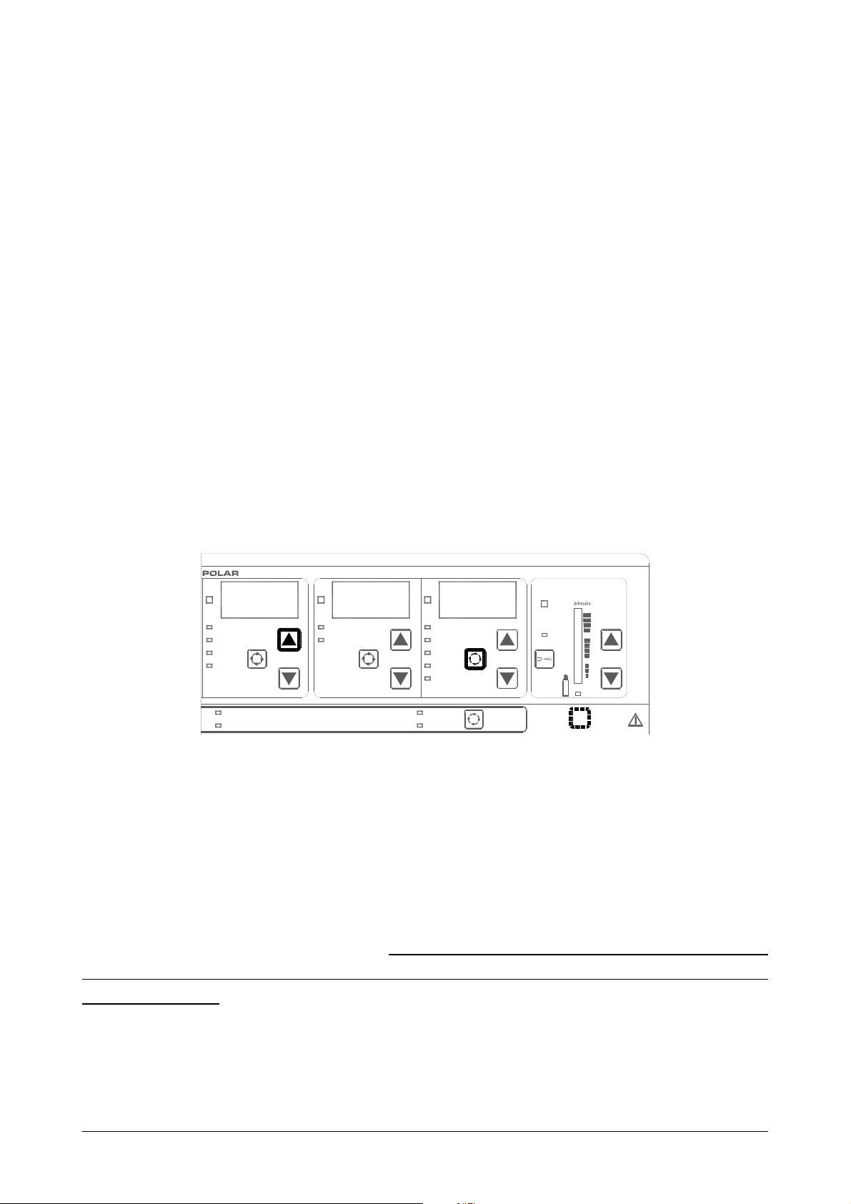
BIPOLAR ARGON
=15
FULG FORCED
PIN POINT CONTACT
SOFT
SPRAY
AN-2
ED-2
MONOPOLAR BIPOLAR
PURE
BLEND
MICRO CV
MICRO HC
MICRO AUTO
MACRO
SEAL HC
BIP-1
BIP-2
10
5
=1
CAL
In the calibration mode, the displays show values in hexadecimal codes, which are different from those
visualized during the normal use; in order to perform any type of calibration, it is necessary to press the
button CAL. At this point, the monopolar section displays start blinking, the light for the setting mode gives a
signal and the bipolar section displays remain switched off. In the monopolar Cut section, the operator sets
the type of test he wants to perform; if the test requires additional parameters, these are selected into the
monopolar Coagulation section. For example, if the operator wants to verify the reading of the A/D inputs
(one of the internal parameters), he will set 01 on the display of the Cut (i.e. reading of the A/D converters)
and a number on the display of the Coagulation related to the input to be read (i.e.: 04 means that the
operator wants to read the A/D input no. 4). During the activation, the result will be visualized on the
monopolar Cut display of the unit; it will be always the monopolar Cut display to be used, independently of
the selected function (example: the reading of a A/D converter that concerns one mode of the bipolar
Coagulation will be set, if necessary, on the interested function, but it will be always visualized on the
monopolar Cut display).
Once selected what has to be calibrated, if further settings about the modality to test are not necessary, it is
sufficient to activate the unit into the function that needs the calibration: automatically, the equipment goes
alsa apparecchi medicali srl 4
Page 5

Excell MCDSe series
Rel. 1
from the visualization of the calibration parameter to the visualization of the power setting (by remaining in
the calibration mode); in order to proceed to the next calibration, it is necessary to press the CAL button
again and go back to the mode of the monopolar section with the blinking displays. The following Table
shows the whole list of the selectable tests:
Monopolar Cut Display
Description
Test n°
00
01
02
03
04
05
06
07
08
09
0b
0C
0d
0E
0F
Reading of the data that come from the analogical inputs of the micro Slave
R.F. leakage current with control made by the software
Start/Stop impedance adjustment for the automatic bipolar mode
Continuous supply of the power stage
Internal parameters of the R.F. section
Functioning of the R.F. section without feed-back
Peak voltage R.F. (Voutpk)
Drain current into the mosfets of the R.F. section
R.F. leakage current without control
Not Used
Visualization of the current software release
Loading of the default values
Reading of the errors memorization
Cancellation of the errors list into the E2PROM
Complete cancellation of the E2PROM
CALIBRATION OF THE POWER SUPPLY SECTION – SETTING OF THE LOW VOLTAGES
Before proceeding with the calibration of the section that controls the supply of the power R.F. generator
stage, it is necessary to verify the continuous low voltages. To do that, connect the positive terminal of a
multimeter to the points indicated in the following Table:
Test Point Voltage (VDC)
L6 +5.08
L7 -15V
L8 +15V
U6 (pin 3) +24V
U13 (pin 3) +5V
Set the R31 pot placed on the Power Supply board (Alsa code: 801471) in order to set exactly the +5V
continuous voltage for the microcontroller section.
CALIBRATION OF THE MASTER MICROCONTROLLER BOARD REFERENCE VOLTAGE
If present, remove the J11 jumper.
Connect a multimeter between the test point J10 and GND; set the R102 pot placed on the Master
Microcontroller board (Alsa code: 801469) in order to obtain a voltage of 5.00V (± 0.01V).
Once the calibration has been performed, close the J11 jumper.
alsa apparecchi medicali srl 5
Page 6

Excell MCDSe series
Rel. 1
CALIBRATION OF THE SLAVE MICROCONTROLLER BOARD REFERENCE VOLTAGE
If present, remove the J12 jumper.
Connect one multimeter between the pin n°2 of J12 and GND; set the R60 pot placed on the Slave
Microcontroller board (Alsa code: 801467) in order to obtain a voltage of 5.00V (± 0.01V).
Once the calibration has been performed, close the J12 jumper.
CALIBRATION OF THE POWER SUPPLY SECTION – SETTING OF THE HIGH VOLTAGE
Press the CAL button; when the displays blink, set the monopolar Cut section, as shown into the Figure:
RAM
MONOPOLAR BIPOLAR
PURE
BLEND-1
FULG FORCED
PIN POINT CONTACT
PURE
BLEND
MICRO CV
MICRO HC
Press the CAL button so that the displays stop blinking. Connect one load of 500ohm/100W to J1 and J2
connectors placed on the Supply board (Alsa code: 801471); connect one multimeter in order to measure
the voltage in parallel to the load. Set the R52 (maximum level) and the R24 (minimum level) pots to obtain
the values shown in the following Table:
Setting Voltage (VDC) Monopolar Coag 05
E6 135,5
0C 8,8
With the blinking displays, and by setting 05 into the monopolar Coagulation section, it is
possible to read the converter A/D “AD5” that sends the value, detected by the
microcontroller, about the supply voltage of the power section.
As these calibrations are interactive, it is advisable to repeat the control of the minimum and maximum
levels at least twice.
CONTROL AND CALIBRATION OF THE INTERNAL PARAMETERS
Press the CAL button; when the displays blink, set the monopolar Cut section, as shown into the Figure:
RAM
MONOPOLAR BIPOLAR
PURE
BLEND-1
FULG FORCED
PIN POINT CONTACT
PURE
BLEND
MICRO CV
MICRO HC
Connect the current probe to one of the conductors of the damping resistor, placed at the bottom of the
metal box.
Press the CAL button so that the displays stop blinking; set 42 in the monopolar Pure Cut mode. Switch the
equipment on: the measured current must be 331mA (± 3%). If the measured value is deeply different with
respect to the one indicated, operate on the loops of the L1 inductor, by changing its position around the
core until the indicated value is obtained (ATTENTION: In order to modify the position of the loops, it is
necessary to take the R.F. generator board away, then make the intervention, and finally place the generator
board again. At this point, repeat the measure).
Set 12 in the bipolar Pure Cut mode; by switching the equipment on, the measured current must be 70mA (±
2mA).
alsa apparecchi medicali srl 6
Page 7

Excell MCDSe series
Rel. 1
CALIBRATION OF THE READING BOARD “VOLTAGE/OUTPUT CURRENT”
The calibration must be performed only when a component of the reading board “voltage/current” is
replaced; in this case, it is advisable to match the board to the new tolerances present in this
section.
Press the CAL button; when the displays blink, set the monopolar Cut section, as shown into the Figure:
RAM
MONOPOLAR BIPOLAR
PURE
BLEND-1
FULG FORCED
PIN POINT CONTACT
PURE
BLEND
MICRO CV
MICRO HC
02 permits the R.F. power delivery without feed-back, by allowing the calibration of the reading section; thanks to the absence of the
feed-back, it is possible to detect directly the influence of the calibrations performed by the operators on the R.F. power delivery, by
avoiding the intervention of the microcontroller that wants to stabilize the power itself.
Press the CAL button again.
Connect the probe of the oscilloscope at the test point indicated with Vref on the R.F. board Output Current
and Voltage board” (Alsa code: 801464). Set the R24 pot in order to obtain a voltage of -2.835V. Connect
the probes of the oscilloscope to the test points indicated with “V” (TP3) and “I” (TP4); set 22 in the
monopolar Pure Cut mode; connect a 400ohms non-inductive load to the active monopolar output. Switch
the unit on and verify that the signals having the probes connected to are in phase. Repeat the same
operation in the bipolar Pure Cut mode, by setting 29 and by connecting a 400ohms load to the active
bipolar output.
Monopolar
Bipolar
Connect a simulation load (composed of a resistance of 250ohm/50W that is connected in parallel to a
capacitor of 1.5nF) at the bipolar output:
R1
20/50W
R2
200/50W
C1
1n5
Connect the oscilloscope probe to the test point indicated with “Phase”; switch the equipment on, by setting
22 in the bipolar Pure Cut mode, and set the R57 pot in order to obtain a voltage of 3.00V.
alsa apparecchi medicali srl 7
Page 8

Excell MCDSe series
=
−==
=
Rel. 1
Set 5 in the monopolar Pure Cut mode, and connect a load 400ohms to the selected monopolar output;
connect the current probe in series to the load, and a voltage probe to the test point indicated with “I-IN”
(TP1). Switch the equipment on, and set the R54 pot: the value read by the voltage probe must be exactly
the double of the current measured by the probe connected in series to the load.
The main aim of this check consists in obtaining an output current of 500mA (in other words, 1.00V at the
test point “I-IN”): to do that, it is necessary to find the better “compromise” between the value of the power
set and the load connected to the output that permits the delivery of this current.
Start by setting 71 in the monopolar Pure Cut mode: switch the equipment on, and change the load at the
output until the current flowing in the load reaches 500mA; connect a probe of the oscilloscope at the test
point indicated with “I-IN” (TP1), and a second probe at the test point “IdB”. Switch the equipment on: the
signal “I-IN” must be 1V. Set the R49 pot: “IdB” must be 0.00V (± 1%). In order to obtain the maximum
reading reliability, set the vertical sensibility at 20mV/div for the reading of “IdB”.
Set 0A in the monopolar Pure Cut mode; switch the equipment on, and set the R61 pot: at the test point
“IdB”, the value must correspond to the logarithm of the voltage measured at the point “I-IN”:
)ln(
VI
INIdB
−
if, for example, the operator obtains a voltage of 110mV when activating the unit, the value to set R61 will
be:
I
dB
Set again in the monopolar Pure Cut mode the value that had permitted before to obtain 500mA of current,
and verify that “IdB” still is 0.00V.
Connect the probes to the test points indicated with “V-IN” and “VdB”; set 52 in the monopolar Pure Cut
mode. By switching the equipment on, the measured value in “V-IN” must be 1.00V; just in case the voltage
is different from this value, change the setting of the power in order to obtain the specified value. Once this
setting has been completed, set the R50 pot to have on “VdB” a signal at 0.00V in correspondence of 1.00V
on “V-IN”. Also in this case, it is advisable to set the sensibility of the oscilloscope at 20mV/div in order to
obtain the maximum reading reliability; moreover, for the measurement of the signals with continuous wave
shape, the operator must reduce the bandwidth on the channel of the oscilloscope in order to eliminate as
much as possible the noises on the low amplitude signals.
Set 05 in the monopolar Pure Cut mode; switch the equipment on, and measure the value at the test point
“V-IN”. Now, activate the unit and set the R62 pot in order to obtain at the test point “VdB” a value that
corresponds to the natural logarithm of “V-IN”:
VV
At the end, verify again if, by setting the power in the Pure Cut mode in order to have “V-IN” at 1.00V, “VdB”
2021100 ,),ln(
)ln(
INVdB
−
still is 0.00V.
Exit from the calibration mode by pressing the combination of the three buttons: calibration, selection of the
bipolar coagulation mode and monopolar coagulation power increase. The operator can also exit by
switching off and then switching on the equipment without pressing any button. Set 100 into the SPRAY
coagulation mode; connect at the selected monopolar output a 350ohms load with the current probe placed
in series to the load. Switch the equipment on, and set the R81 pot in order to calibrate the value of the
power supplied according to what had been set. Notably, a power of 100W corresponds to a current of
alsa apparecchi medicali srl 8
Page 9

Excell MCDSe series
R
Rel. 1
535mA on the load indicated before. Check the right supply of power, by setting also other lower values and,
if necessary, set the R81 pot again.
Set the Auto Pure monopolar function at 200; at the selected monopolar output, connect a 200ohms load;
switch the equipment on, and set the R30 pot in order to obtain an output current of 1.0A. Verify the
correspondence existing between the selection and the R.F. power delivery, even in the Pure Cut mode and
in the bipolar Blend mode.
MATCHING OF THE POWER MOSFETS DRAIN CURRENT
Press the CAL button; when the displays blink, set the monopolar Cut section, as shown into the Figure:
AM
MONOPOLAR BIPOLAR
PURE
BLEND-1
FULG FORCED
PIN POINT CONTACT
PURE
BLEND
MICRO CV
MICRO HC
Press the CAL button in order to interrupt the displays blinking, and set 35 in the SPRAY mode. Connect a
200ohms non-inductive load at the output of the equipment. Connect the probes of the oscilloscope to the
signals indicated with DRIVRF and IPKISOG on the R.F. power generator board (Alsa code: 801465), and
check the following waveforms:
Just in case the signals measured by the probes are different, it is necessary to change the position of the
jumpers connections J1 and J4, placed on the R.F. power generator board (from horizontal to vertical
position, and vice versa). At the end, put the R.F. power generator board in its right position.
CALIBRATION OF THE OUTPUT VOLTAGE PEAK FOR EACH MODE
Press the CAL button; when the displays blink, set the monopolar Cut section, as shown into the Figure:
MONOPOLAR BIPOLARRAM
PURE
BLEND-1
Press the CAL button in order to interrupt the displays blinking.
Connect the high voltage probe to the selected output; in order to perform this calibration, it is necessary to
use standard length cables connected to the output (even better if placed according to the Standard CEI EN
alsa apparecchi medicali srl 9
FULG FORCED
PIN POINT CONTACT
PURE
BLEND
MICRO CV
MICRO HC
Page 10

Excell MCDSe series
R
Rel. 1
60601-2-2 – art. 6.8.3 Technical Description, point cc). By switching each single function on, and by
operating on the buttons of power increase/decrease, it is possible to adjust the maximum value of the peak
voltage. The values of these voltages are illustrated in the following Table:
Function Minimum Value Maximum Value
Monopolar Functions
Pure 3300* 3600
Blend 1 3400 3650
Blend 2 7600 7700
Endo 1600 1900
Fulg Forced 4500 4800
PinPoint Contact 3400 3500
Soft 3400 3500
Spray 7500 7800
Bipolar Functions
Pure 700 840
Blend 880 980
Micro 400 430
Macro 700 760
NOTE: Into the Table, the bipolar function of MICRO AUTO does not appear because it delivers the same
voltage as the function MICRO.
CALIBRATION OF THE MAXIMUM POWER STAGE MOSFETS CURRENT FOR EACH
FUNCTION
Press the CAL button; when the displays blink, set the monopolar Cut section, as shown into the Figure:
AM
Press the CAL button in order to interrupt the displays blinking.
The calibration of the maximum current must be performed in each single function, by setting its maximum
level. During the activation, operate on the buttons of power increase/decrease, in order to obtain the current
values indicated in the following Table:
MONOPOLAR BIPOLAR
PURE
BLEND-1
FULG FORCED
PIN POINT CONTACT
PURE
BLEND
MICRO CV
MICRO HC
alsa apparecchi medicali srl 10
Page 11

Excell MCDSe series
R
R
Rel. 1
Monopolar Function
50ohm
100ohm
150ohm
min max min max min max
Pure Cut 150 1.68 1.44 1.48 1.28 1.35
Blend 1 1.64 1.68 1.44 1.46 1.37 1.39
Blend 2 1.40 1.46 1.04 1.06
Endo 1.35 1.49 1.19 1.28 1.11 1.21
Fulg Forced 1.48 1.55 1.11 1.15 0.92 0.95
PinPoint Contact 1.57 1.58 1.40 1.46 1.24 1.26
Monopolar Function
50ohm
100ohm
150ohm
Soft 1.50 1.53 1.32 1.36 1.21 1.26
Spray 1.41 1.46 1.04 1.06 0.88 0.89
Bipolar Function
10ohm
50ohm
100ohm
min max min max min max
Pure Cut 2.58 2.7 1.51 1.56 1.13 1.18
Blend 2.34 2.42 1.44 1.48 1.07 1.10
Micro 2.39 2.43 1.44 1.47 1.07 1.10
Macro 2.39 2.43 1.44 1.46 1.07 1.10
CONTROL OF THE H.F. LEAKAGE CURRENTS
Press the CAL button; when the displays blink, set the monopolar Cut section, as shown into the Figure:
AM
Press the CAL button in order to interrupt the displays blinking.
For each function of the equipment, it is necessary to adjust the limit of the R.F. leakage current. To do that,
connect the equipment under test to a system for the measurement of the high frequency leakage currents;
then, switch every single function and operate on the buttons of power increase/decrease, in order to bring
the registered value within the limits established by the Standard (lower than 150mA for monopolar – less
than 1% of maximum power for bipolar).
CALIBRATION OF THE OUTPUT CURRENT
Press the CAL button; when the displays blink, set the monopolar Cut and Coagulation section, as shown
into the Figure:
MONOPOLAR BIPOLAR
PURE
BLEND-1
FULG FORCED
PIN POINT CONTACT
PURE
BLEND
MICRO CV
MICRO HC
AM
MONOPOLAR BIPOLAR
PURE
BLEND-1
FULG FORCED
PIN POINT CONTACT
PURE
BLEND
MICRO CV
MICRO HC
Connect at the bipolar output a 200ohms non-inductive load with the current probe placed in series to the
load. Activate the bipolar Pure Cut mode. The setting values are reported in the following table. During the
switching on, operate on the buttons of power increase/decrease, in order to obtain the correspondent
alsa apparecchi medicali srl 11
Page 12

Excell MCDSe series
Rel. 1
values, as indicated in the column “I-Out”; if necessary, use the R1 pot placed on the main board (Alsa code
801463) in order to obtain the right H.F. current values on the load, as indicated in the column “Current”:
Setting Current (A) I-Out (Hex)
31
47
71
9d
0.22
0.32
0.50
0.70
24
34
54
75
CALIBRATION OF THE NEUTRAL PLATE CIRCUIT
Connect the probe of the oscilloscope to the point indicated with TP2 on the board for the hand-switch
control (Alsa code: 801462).
Connect a 250ohms resistor to the terminals of the neutral plate.
Calibrate the R27 pot in order to obtain a sinusoidal waveform, which is symmetric with respect to the
horizontal axis. The following Figures show an example of right and wrong waveform:
Wrong Right
NOTE: The points indicated with “start” and “end” must coincide as much as possible with the X axis.
At the end of the calibration, the frequency of the sinusoidal wave is about 100kHz; anyway, it must be said
that the calibration establishes the exact “coupling point” of the neutral plate circuit, while the frequency
represents its natural consequence.
The control circuit of the contact between the plate and the patient verifies the condition for an optimum
contact as well as some intermediate levels, which are shown to the operator through the lights, placed into
the section indicated on the panel with “N.P.”. Notably, we can distinguish the following cases:
1) from 0 to 160 ohms: optimum contact. All the luminous signals that concern the neutral plate are
switched off. The equipment can be used by setting any power, and the supply will correspond to
what has been set;
2) from 160 to 190 ohms: the quality of the contact begin to decrease. The first luminous signal lights
up in order to inform the operator on the current status of the contact;
3) from 190 to 250 ohms: the quality of the contact worsens considerably. Also the second luminous
signal lights up in order to capture the attention of the operator. Besides this threshold, the
alsa apparecchi medicali srl 12
Page 13

Excell MCDSe series
Rel. 1
equipment will automatically reduce the output power delivered to 50%, in order to avoid all risks of
burns due to a bad contact between the plate and the patient;
4) from 250 to 380 ohms: the quality of the contact does not allow the delivery of the electrosurgical
unit maximum power anymore. Besides the luminous signals mentioned above, there is also here a
blinking red light, which tells the operator that something is going wrong;
5) more than 380 ohms: the contact between the plate and the patient is definitely not enough. The red
light remains lit; the equipment gives an intermittent acoustic alarm signal, and on the display the
message no nP appears. The equipment interrupts the output power delivery until the quality of the
contact is re-settled again.
Set the R40 pot placed on the board for the Handle Control (Alsa code: 801462), by using a simulation
potentiometer connected to the terminals of the neutral plate, in order to allow the unit functioning as
described above.
SECTION FOR THE ARGON GAS COAGULATOR
Connect the cylinder at the rear input, and adjust the pressure until the light for the absence of gas is
switched off. The recommended input pressure is 2.5-3 bar. The activation of this section is possible only
when the input pressure is considered adequate for the use. By the contrary, it is not possible when:
• the input pressure is not sufficient at all (the red light placed under the setting bar for the output flow
lights up);
• the input pressure is too high (the equipment shows the alarm signal HI PrS).
By pressing the button indicated with:
the coagulator section is activated; at this point, the unit performs a short selftest for this specific section. If
no anomaly is present, the equipment is ready for the use of the Argon gas; the operator must set the
desired flow level, by using the increase/decrease buttons. At the same time, the luminous signal for the
activation of the SPRAY coagulation and the one for the radiofrequency output to be used start blinking. At
the switching on, the indication will show exactly the flow supplied, and not simply the level that had been
set.
In order to verify this action, first of all it is necessary to test the status of the control board. To do that,
switch the equipment on, and on the board with Alsa code 801468 (Argon Management board) verify what
follows:
• Vref on J7: the multimeter must indicate 10V (± 0.1V); if not, set the R40 pot of the board with Alsa
code: 801468;
• the offset of the input pressure sensor on J2: the multimeter must indicate 0V (± 0.01V); if not, set
the R26 pot;
• the offset of the input pressure sensor on J3: the multimeter must indicate 0V (± 0.01V); if not, set
the R39 pot.
The control of the Argon gas supply is possible by using a flowmeter with full scale of about 20lt/min, and a
manometer with full scale of about 3bar.
By connecting the Argon supply handle to the output of the unit, check the correspondence between the flow
set and the flow supplied. If necessary, set the screw regulator placed at the output of the pressure reducer,
alsa apparecchi medicali srl 13
Page 14

Excell MCDSe series
Rel. 1
which is inside the equipment. The adjustment can have a tolerance of 20%. Verify that the output pressure
does not exceed 2 bars. The nominal value is around 1.5 bars.
LIST OF THE ERROR CODES
In order to facilitate the technical assistance, an error code for each anomaly is memorized inside the
2
PROM; thanks to a particular procedure, which can be selectable exclusively in the calibration mode, it is
E
possible to visualize the last 32 errors that occurred to the unit. It is also possible to cancel this list, in order
to avoid repeated checks when the equipment is switched on again.
HOW READING THE LIST OF THE ERRORS
To visualize the list of the errors, it is necessary to enter into the calibration mode, by pressing at the same
time the three buttons: CAL, selection of the bipolar coagulation mode, and increase of the monopolar
coagulation power. After the appearance of the signal message about the calibration status on the display
(CAL on), press the CAL button again, and, with the blinking displays, select 0d into the monopolar Cut
section and a number from 00 to 20 (from 0 to 20 in the hexadecimal scale corresponds to 32 positions in
the decimal scale) into the monopolar coagulation section (the latter represents the number of the
memorized error; the last error that has occurred is indicated by the signal on the Cut display that will be
FF). By pressing the monopolar Cut activation pedal-switch, the error code about the position selected
before with the monopolar Coagulation section will appear.
HOW DELETING THE LIST OF THE MEMORIZED ERRORS
Always in the calibration mode, press the CAL button and, with the blinking displays, select 0E into the
monopolar Cut section; by pressing the monopolar Cut activation pedal-switch, the display will show the
code E2P CLr, to inform the operator that the memories for the errors have been deleted. By repeating the
reading sequence of the errors (see the previous paragraph), all the memories will contain FF.
alsa apparecchi medicali srl 14
Page 15

Excell MCDSe series
Rel. 1
Type of Error
Errors of setting or on the activation circuits
Anomaly on the neutral plate
Error registered into the neutral plate circuit
Error on the control circuit of the plate/tissue contact
Error on the hand-switch activation circuit at the switching on
Error on the pedal-switch activation circuit at the switching on
Simultaneous activation of two devices not allowed
Error on the keyboard registered during the self test
Errors on the Argon gas section
Input pressure of the Argon gas too high
Error in the Argon gas section during the Argon selection
Loss of Argon gas due to an internal leakage
Pressure of the Argon gas not sufficient during the activation
Activation of the Argon input placed backside during the
switching on
Code
Code memorized in E2PROM
(in CAL mode, select “0d”)
no nP
Err nPC 81
Err 53 35
Err Hnd 82
Err PEd 83
USr Act 85
Err 14 0E
HI PrS 88
Err 30 1E
Err 31 1F
Err 29 1d
Err Ein 84
1
-
Errors on the Master microcontroller
RAM memory
FLASH memory
Complemented variables of the system
Errors on the power supply section
Watchdog Timer
Error +5V
Error of the R.F. power supply with lower setting value
Error of the R.F. power supply with higher setting value
R.F. power supply higher than the pre-set value during the
activation phase
Errors on the serial communication
Error on the serial communication peripherals placed on the
main board (Alsa code: 801463)
Error on the serial communication peripheral placed on the
power supply board (Alsa code: 801471)
Err 32 20
Err 34 22
Err 35 23
Err 33 21
Err 36 24
Err 37 25
Err 38 26
Err 97 61
2 slow acoustic
repetitions and then rapid
intermittence
3 slow acoustic
repetitions and then rapid
intermittence
3d
3E
1
According to the numerical indication of error which appears on the display when an anomaly occurs, the hexadecimal value
correspondent to one of the Error Codes shown in the column Code is memorized inside the E
2
PROM.
alsa apparecchi medicali srl 15
Page 16

Type of Error
Error on the serial communication peripheral placed on the
hand-switch control board (Alsa code: 801462)
Error in the communication with the E2PROM 5 slow acoustic
Absence of connection I2CBUS (during the use) 6 slow acoustic
Non Master-Slave connection (during the self test) 7 slow acoustic
Error on the Slave microcontroller 8 slow acoustic
repetitions and then rapid
repetitions and then rapid
repetitions and then rapid
repetitions and then rapid
repetitions and then rapid
Errors on the Slave microcontroller
Error on a Slave microcontroller internal peripheral
Errors on the R.F. power section
Error in the internal dummy load used during the self test
Error in the R.F. output power measurement circuit (with lower
setting value
Error in the R.F. output power measurement circuit (with higher
setting value)
Error in the bipolar power circuit with lower setting value
Error in the bipolar power circuit (with higher setting value)
Error of functioning in the monopolar circuit in the PURE mode
Error of functioning in the monopolar circuit in the SPRAY
mode
Error on the modulation signal of the function BLEND-1
Error on the modulation signal of the function FULG FORCED
Error on the modulation signal of the function SPRAY
Error in the reading of the output peak voltage (with lower
setting value
Error in the reading of the output peak voltage (with higher
setting value)
Error in the reading of the output peak current (with lower
setting value
Error in the reading of the output peak current (with higher
setting value)
HF output power higher than expected
Errors on the thermal protections
Thermal protection of the power supply unit
Thermal protection of the R.F. power section
Code
4 slow acoustic
intermittence
intermittence
intermittence
intermittence
intermittence
Err 60 3C
Err 39 27
Err 51 33
Err 52 34
Err 43 2b
Err 42 2A
Err 40 28
Err 41 29
Err 44 2C
Err 45 2d
Err 46 2E
Err 47 2F
Err 48 30
Err 49 31
Err 50 32
Err 98 62
Err 27 1b
Err 28 1C
Excell MCDSe series
Rel. 1
Code memorized in E2PROM
(in CAL mode, select “0d”)2
3F
40
43
41
44
2
According to the numerical indication of error which appears on the display when an anomaly occurs, the hexadecimal value
correspondent to one of the Error Codes shown in the column Code is memorized inside the E
2
PROM.
alsa apparecchi medicali srl 16
Page 17

TEST POINTS LIST
TP1: NP Dr i ving signal frequency
TP2: NP Driving signal
TP3: NP Coupling level
TP4: NP blinking led
TP5: Handswitch driving signal
+5VF
R80
NU
+15VF
R81
-15VF
NU
NU
R82
D21
D19
D20
.
.
.
+15V
-15V
+5V
47UH/0.7A
47UH/0.7A
47UH/0.7A
GND1
+5VF VDC
R2
R1
5K6_SMD
U6
5K6_SMD
PCF8574_SMD
13
INT
15
SDA
14
SCL
1
A0
. .
2
A1
3
A2
+5VF
U5B
3 4
74HCT14_SMD
N/P OK
VDD
+5VF
U7
OPI1264B
12
3 4
+5VF
U8
OPI1264B
12
3 4
+5VF
U9
OPI1264B
12
3 4
+5VF
U10
OPI1264B
12
3 4
J3
1
ENHND1
GND
2
ENHND2
3
GND
4
RLSFLT2
5
LEDNP
6
ENBIPAUT
7
REMLEV
8
INTIIA
9
+15V
10
11
12
+5V
13
-15V
14
PICO_14
C2
1U_SMD_1210
.
P0
P1
P2
P3
P4
P5
P6
P7
/AUTBIP
R26
3K3_SMD
U5F
13 12
R10
1K_SMD
R11
1K_SMD
R12
1K_SMD
R13
1K_SMD
To Power Supply Board
V1
CUT1
4
COAG1
5
CUT2
6
COAG2
7
9
10
11
12
D4
5V1_SMD
.
74HCT14_SMD
.
U5E
11 10
74HCT14_SMD
U5D
.
9 8
74HCT14_SMD
.
U5C
5 6
74HCT14_SMD
.
alsa apparecchi medicali s.r.l.
To power supply
Board
SDA
SCL
To front Panel
Board
+5VFVDD
J1
1
2
3
4
J2
1
2
3
4
.
C9
1U_SMD_1210
..
.
1U_SMD_1210
+15VF
2
5
C1
C11
100N_SMD
R39
TR
CV
4
8K2/1%_SMD
NU
+15VF
R
NE555_SMD
R35
8
1
.
VCC
GND
5KT/L/10G
390/1%_SMD
THR
U1
DIS
560_SMD
Q
2N2_SMD
R40
R45
TP1
R4
3
R24
7
3K3_SMD
R27
6
5KT/L/10G
C25
+15VF
3
LM324_SMD
2
C10
100N_SMD
R6
1K_SMD
-15VF
C4
R15
1U_SMD_1210
10K_SMD
C13
411
.
100N_SMD
1
U3A
.
R46
1K5/1%_SMD
.
C26
1n/1%_SMD
L1
+15VF
C27
47u/E/35V
.
L2
-15VF
C28
47u/E/35V
.
L3
+5VF
C29
47u/E/35V
.
R55
4K7_SMD
R44
2K2_SMD
.
R49
10_SMD
R3
5K6_SMD
R54
4K7_SMD
100p/1%_SMD
5
7
6
16
3
4
2
1
9
C24
.
R5
1K_SMD
.
3
.
1U_SMD_1210
.
1U_SMD_1210
CT
DIS
RT
VREF
SYNC
OSC.OUT
NI INP
INV INP
COMP
C23
100p/1%_SMD
G
IN6VL
ADG419_SMD
V-7V+
C5
C7
SS
8
100N_SMD
TP2
T1
PN 1
1
2 3
.
.
R31
1K_SMD
.
18sp
3E25NP
R32
1K_SMD
R25
3K3_SMD
R28
10K_SMD
R29
100K_SMD
12
13
TP5
1
2
14sp
3E25HND
10
T2
4
6sp
LM324_SMD
9
PN 2
5
6
U3D
LM324_SMD
U3B
LM324_SMD
330K_SMD
330K_SMD
6
8sp8sp
5
4
3
R36
R37
R30
12K_SMD
U3C
1N4148_SMD
1N4148_SMD
R16
INTIIA
100_SMD
R17
SDA
100_SMD
SCL
100_SMD
R18
R19
7
100_SMD
14
R41
1K5_SMD
R42
1K5_SMD
8
N/S
D8
RFHND1
C17
100N_SMD
RFHND2
D9
C19
100N_SMD
R7
5V1_SMD
.
1K_SMD
.
1N4148_SMD
1N4148_SMD
D5
REMLEV
D3
5V1_SMD
D6
1 2
D7
1U_SMD_1210
CTHND1
CGHND1
CTHND2
CGHND2
R38
330K_SMD
C6
U5A
74HCT14_SMD
L5
L6
L7
L4
ENBIPAUT
R34
220_SMD
R43
2K2_SMD
1K_SMD
LEDNP
+5VF
100_SMD_1206
C15
100N_SMD
100_SMD_1206
C18
100N_SMD
100_SMD_1206
C20
100N_SMD
100_SMD_1206
C21
100N_SMD
R33
R8
220_SMD
C12
100N_SMD
.
+5VF
TP4
R20
C14
R50
100N_SMD
150_SMD
R21
C16
R51
100N_SMD
150_SMD
R22
C30
R52
100N_SMD
150_SMD
R23
C31
100N_SMD
R53
150_SMD
D1
R14
10K_SMD
1
2
D
S1
S2
+15VF
8
15V_SMD
D2
15V_SMD
U2
5
C3
4
.
1U_SMD_1210
R9
1K_SMD
N/S
TP3
+15VF
R47
10_SMD
13
15
VC
+VIN
U4
UC3525_SMD
OUT A
OUT B
SHUNT
C8
1U_SMD_1210
R48
11
10_SMD
14
10
GND
12
GNDVSS
C22
.
CTHND1
RFHND1
CGHND1
CTHND2
RFHND2
CGHND2
SwitchOver Section
CTHND1
RFHND1
CGHND1
CTHND2
RFHND2
CGHND2
PN 1
PN 2
+15VF
GND
ENHND1
ENHND2
RLSFLT2
bismy 0 3 rele.schdoc
PN 1
PN 2
+15VF
GND
ENHND1
ENHND2
RLSFLT2
EXCELL MCDSe
Double Handswitch & NP control board
BisMy03HandleSwitch.Schdoc
alsa code: 801462
Drawn by:
Rel.: 3.5 24/11/2008
Approval:
Page 18

R60
+15VF
+15VF
R61
J6
ENHND1
RFHND1
ENHND2
RFMONIL
ENHND1
ENHND2
RLSFLT2
+15VF
GND
ENHND1
ENHND2
RLSFLT2
+15VF
GND
R67
R69
D14
R56
C32
D10
Q1
1 2
3
RL1
ENREL1
4
5
R64
+15VF
ENHND1
D11
R68
C33
R57
...
+15VF
R62
R63
D16
D13
C35
R58
C34
D12
1 2
3
ENREL2
4
5
RL3
R65
+15VF ENREL2
ENHND2
R70
R59
...
D18
.
C36
RFMONP
J7
PN 1
PN 2
RL5
*
1 8
*
*
3
6
SGR282Z
R66
2
4
7
5
R71
+15VFRLSFLT2
J10
J11
PN 2
C37
D15
1 2
Q2
*
4
3
5
RL2
...
+15VF
D17
1 2
Q4Q3
4
3
5
RL4
...
TO NEUTRAL PLATE
ENREL1
RFMONIL
RFHND2
J12
Switch-over s e ction
bismy03 rele.schdoc
alsa code: 801462
Drawn by:
J4
RFHND1
CGHND1
CTHND1
J5
RFHND2
CGHND2
CTHND2
J8
OUT
CG
CT
J9
OUT
CG
CT
CTHND1
RFHND1
CGHND1
CTHND2
RFHND2
CGHND2
PN 1
PN 2
alsa apparecchi medicali s.r.l.
EXCELL MCDSe
Rel.: 3.5 24/11/2008
Approval:
HANDLE1HANDLE2
CTHND1
RFHND1
CGHND1
CTHND2
RFHND2
CGHND2
PN 1
PN 2
Page 19

Page 20

File name: Double handswitch & NP control board alsa code: [801462] Rev.: [3.5]
Date: Nov 24, 2008
Ref. Part Type Description alsa code
__________________________________________________________________________
R1 5K6_SMD STANDARD CHIP RESISTOR 430512/S
R2 5K6_SMD STANDARD CHIP RESISTOR 430512/S
R3 5K6_SMD STANDARD CHIP RESISTOR 430512/S
R4 560_SMD STANDARD CHIP RESISTOR 430500/S
R5 1K_SMD STANDARD CHIP RESISTOR 430502/S
R6 1K_SMD STANDARD CHIP RESISTOR 430502/S
R7 1K_SMD STANDARD CHIP RESISTOR 430502/S
R8 1K_SMD STANDARD CHIP RESISTOR 430502/S
R9 1K_SMD STANDARD CHIP RESISTOR 430502/S
R10 1K_SMD STANDARD CHIP RESISTOR 430502/S
R11 1K_SMD STANDARD CHIP RESISTOR 430502/S
R12 1K_SMD STANDARD CHIP RESISTOR 430502/S
R13 1K_SMD STANDARD CHIP RESISTOR 430502/S
R14 10K_SMD STANDARD CHIP RESISTOR 430513/S
R15 10K_SMD STANDARD CHIP RESISTOR 430513/S
R16 100_SMD STANDARD CHIP RESISTOR 430496/S
R17 100_SMD STANDARD CHIP RESISTOR 430496/S
R18 100_SMD STANDARD CHIP RESISTOR 430496/S
R19 100_SMD STANDARD CHIP RESISTOR 430496/S
R20 100_SMD_1206 STANDARD CHIP RESISTOR 430540/S
R21 100_SMD_1206 STANDARD CHIP RESISTOR 430540/S
R22 100_SMD_1206 STANDARD CHIP RESISTOR 430540/S
R23 100_SMD_1206 STANDARD CHIP RESISTOR 430540/S
R24 3K3_SMD STANDARD CHIP RESISTOR 430508/S
R25 3K3_SMD STANDARD CHIP RESISTOR 430508/S
R26 3K3_SMD STANDARD CHIP RESISTOR 430508/S
R27 5KT/L/10G PRESET POTENTIOMETER MULTITURN 403123
R28 10K_SMD STANDARD CHIP RESISTOR 430513/S
R29 100K_SMD STANDARD CHIP RESISTOR 430528/S
R30 12K_SMD STANDARD CHIP RESISTOR 430515/S
R31 1K_SMD STANDARD CHIP RESISTOR 430502/S
R32 1K_SMD STANDARD CHIP RESISTOR 430502/S
R33 220_SMD STANDARD CHIP RESISTOR 430497/S
R34 220_SMD STANDARD CHIP RESISTOR 430497/S
R35 8K2/1%_SMD 1% PRECISION CHIP RESISTOR 430539/S
R36 330K_SMD STANDARD CHIP RESISTOR 430537/S
R37 330K_SMD STANDARD CHIP RESISTOR 430537/S
R38 330K_SMD STANDARD CHIP RESISTOR 430537/S
R39 NU NOT USED -----R40 5KT/L/10G PRESET POTENTIOMETER MULTITURN 403123
R41 1K5_SMD STANDARD CHIP RESISTOR 430503/S
R42 1K5_SMD STANDARD CHIP RESISTOR 430503/S
R43 2K2_SMD STANDARD CHIP RESISTOR 430506/S
R44 2K2_SMD STANDARD CHIP RESISTOR 430506/S
R45 390/1%_SMD 1% PRECISION CHIP RESISTOR 430538/S
R46 1K5/1%_SMD 1% PRECISION CHIP RESISTOR 430504/S
R47 10_SMD STANDARD CHIP RESISTOR 430493/S
R48 10_SMD STANDARD CHIP RESISTOR 430493/S
R49 10_SMD STANDARD CHIP RESISTOR 430493/S
R50 150_SMD STANDARD CHIP RESISTOR 430531/S
R51 150_SMD STANDARD CHIP RESISTOR 430531/S
R52 150_SMD STANDARD CHIP RESISTOR 430531/S
R53 150_SMD STANDARD CHIP RESISTOR 430531/S
R54 4K7_SMD STANDARD CHIP RESISTOR 430511/S
R55 4K7_SMD STANDARD CHIP RESISTOR 430511/S
R56 10K_SMD STANDARD CHIP RESISTOR 430513/S
R57 10K_SMD STANDARD CHIP RESISTOR 430513/S
R58 10K_SMD STANDARD CHIP RESISTOR 430513/S
R59 10K_SMD STANDARD CHIP RESISTOR 430513/S
R60 NU NOT USED -----R61 NU NOT USED -----R62 NU NOT USED -----R63 NU NOT USED -----R64 47_SMD STANDARD CHIP RESISTOR 430495/S
R65 47_SMD STANDARD CHIP RESISTOR 430495/S
R66 0/0_SMD STANDARD CHIP RESISTOR 0 OHMS 430579/S
R67 4K7_SMD STANDARD CHIP RESISTOR 430511/S
R68 4K7_SMD STANDARD CHIP RESISTOR 430511/S
R69 4K7_SMD STANDARD CHIP RESISTOR 430511/S
1
Page 21

File name: Double handswitch & NP control board alsa code: [801462] Rev.: [3.5]
Date: Nov 24, 2008
Ref. Part Type Description alsa code
__________________________________________________________________________
R70 4K7_SMD STANDARD CHIP RESISTOR 430511/S
R71 680_SMD STANDARD CHIP RESISTOR 430501/S
R80 NU NOT USED -----R81 NU NOT USED -----R82 NU NOT USED -----C1 1U_SMD_1210 CERAMIC CHIP CAPACITOR 400326/S
C2 1U_SMD_1210 CERAMIC CHIP CAPACITOR 400326/S
C3 1U_SMD_1210 CERAMIC CHIP CAPACITOR 400326/S
C4 1U_SMD_1210 CERAMIC CHIP CAPACITOR 400326/S
C5 1U_SMD_1210 CERAMIC CHIP CAPACITOR 400326/S
C6 1U_SMD_1210 CERAMIC CHIP CAPACITOR 400326/S
C7 1U_SMD_1210 CERAMIC CHIP CAPACITOR 400326/S
C8 1U_SMD_1210 CERAMIC CHIP CAPACITOR 400326/S
C9 1U_SMD_1210 CERAMIC CHIP CAPACITOR 400326/S
C10 100N_SMD CERAMIC CHIP CAPACITOR 400320/S
C11 100N_SMD CERAMIC CHIP CAPACITOR 400320/S
C12 100N_SMD CERAMIC CHIP CAPACITOR 400320/S
C13 100N_SMD CERAMIC CHIP CAPACITOR 400320/S
C14 100N_SMD CERAMIC CHIP CAPACITOR 400320/S
C15 100N_SMD CERAMIC CHIP CAPACITOR 400320/S
C16 100N_SMD CERAMIC CHIP CAPACITOR 400320/S
C17 100N_SMD CERAMIC CHIP CAPACITOR 400320/S
C18 100N_SMD CERAMIC CHIP CAPACITOR 400320/S
C19 100N_SMD CERAMIC CHIP CAPACITOR 400320/S
C20 100N_SMD CERAMIC CHIP CAPACITOR 400320/S
C21 100N_SMD CERAMIC CHIP CAPACITOR 400320/S
C22 100N_SMD CERAMIC CHIP CAPACITOR 400320/S
C23 100p/1%_SMD 1% CERAMIC CHIP CAPACITOR 400316/S
C24 100p/1%_SMD 1% CERAMIC CHIP CAPACITOR 400316/S
C25 2N2_SMD CERAMIC CHIP CAPACITOR 400325/S
C26 1n/1%_SMD 1% CERAMIC CHIP CAPACITOR 400318/S
C27 47u/E/35V VERTICAL ELECTROLYTIC CAPACITOR 400237
C28 47u/E/35V VERTICAL ELECTROLYTIC CAPACITOR 400237
C29 47u/E/35V VERTICAL ELECTROLYTIC CAPACITOR 400237
C30 100N_SMD CERAMIC CHIP CAPACITOR 400320/S
C31 100N_SMD CERAMIC CHIP CAPACITOR 400320/S
C32 100n_SMD CERAMIC CHIP CAPACITOR 400320/S
C33 100N_SMD CERAMIC CHIP CAPACITOR 400320/S
C34 100n_SMD CERAMIC CHIP CAPACITOR 400320/S
C35 100n_SMD CERAMIC CHIP CAPACITOR 400320/S
C36 100N/PP/250V POLYPROPYLENE CAPACITOR 400321
C37 100N/PP/250V POLYPROPYLENE CAPACITOR 400321
D1 15V_SMD SMD ZENER DIODE 420104/S
D2 15V_SMD SMD ZENER DIODE 420104/S
D3 5V1_SMD SMD ZENER DIODE 420101/S
D4 5V1_SMD SMD ZENER DIODE 420101/S
D5 5V1_SMD SMD ZENER DIODE 420101/S
D6 1N4148_SMD SMD DIODE 420098/S
D7 1N4148_SMD SMD DIODE 420098/S
D8 1N4148_SMD SMD DIODE 420098/S
D9 1N4148_SMD SMD DIODE 420098/S
D10 NU NOT USED -----D11 NU NOT USED -----D12 NU NOT USED -----D13 NU NOT USED -----D14 1N4148_SMD SMD DIODE 420098/S
D15 1N4148_SMD SMD DIODE 420098/S
D16 1N4148_SMD SMD DIODE 420098/S
D17 1N4148_SMD SMD DIODE 420098/S
D18 1N4148_SMD SMD DIODE 420098/S
Q1 BC817_SMD SMD NPN TRANSISTOR 427089/S
Q2 BC817_SMD SMD NPN TRANSISTOR 427089/S
Q3 BC817_SMD SMD NPN TRANSISTOR 427089/S
Q4 BC817_SMD SMD NPN TRANSISTOR 427089/S
U1 NE555_SMD SMD TIMER NE555 482135
U2 ADG419_SMD SMD SINGLE ANALOG SWITCH 482116
U3 LM324_SMD SMD QUAD OP AMP LM324 482127
U4 UC3525_SMD SMD PWM UC3525 482136
U5 74HCT14_SMD SMD HEX INVERTERS WITH SCHMITT TRIGGER 482106
2
Page 22

File name: Double handswitch & NP control board alsa code: [801462] Rev.: [3.5]
Date: Nov 24, 2008
Ref. Part Type Description alsa code
__________________________________________________________________________
U6 PCF8574_SMD SMD II_CBUS I/O EXPANDER 482128
U7 OPI1264B OPTOCOUPLER 420110
U8 OPI1264B OPTOCOUPLER 420110
U9 OPI1264B OPTOCOUPLER 420110
U10 OPI1264B OPTOCOUPLER 420110
L1 47UH/0.7A INDUCTOR 422009
L2 47UH/0.7A INDUCTOR 422009
L3 47UH/0.7A INDUCTOR 422009
L4 1MH/100MA INDUCTOR 422005
L5 1MH/100MA INDUCTOR 422005
L6 1MH/100MA INDUCTOR 422005
L7 1MH/100MA INDUCTOR 422005
T1 3E25NP NEUTRAL PLATE CIRCUIT TRANSFORMER 714181
T2 3E25HND TRANSFORMER FOR HANDLE ACTIVATION 714180
RL1 V23061 1 CHANGEOVER RELAY 404044
RL2 V23061 1 CHANGEOVER RELAY 404044
RL3 V23061 1 CHANGEOVER RELAY 404044
RL4 V23061 1 CHANGEOVER RELAY 404044
RL5 SGR282Z 2 CHANGEOVER RELAY 404048
J1 PICO_4 4 POLES PICOFLEX CONN. MALE P.C.B. 384042
J2 PICO_4 4 POLES PICOFLEX CONN. MALE P.C.B. 384042
J3 PICO_14 14 POLES PICOFLEX CONN. MALE P.C.B. 384040
J6 399030 4.8 MM FASTON CONNECTOR P.C.B. 399030
J7 399030 4.8 MM FASTON CONNECTOR P.C.B. 399030
J10 399030 4.8 MM FASTON CONNECTOR P.C.B. 399030
J11 399030 4.8 MM FASTON CONNECTOR P.C.B. 399030
J12 399030 4.8 MM FASTON CONNECTOR P.C.B. 399030
3
Page 23

R87
2K2_SMD_2512
2K2_SMD_2512
C34
4u7
IPKISOG
C3
100p
IPKISOGND
C11
10p
LZ
R24
R25
2K2_SMD_2512
C19
100p
J15
1
ENHND1
2
RLSLFT2
3
ENHND2
TERMRF
4
5
+5V
6
+5V
7
INTIIA
8
ENBIPAUT
9
+15V
10
+15V
GND
11
GND
12
13
-15V
14
To Power supply board
+5V
+5V
C32
4u7
R38
10K
47uH/0.7A
GND
.
R27
1K
L3
VSS
R8
2K2
R2
470
C16
1n/C/3KV
C33
1u
RL1
MONO
1 8
+15V
+5V
D1
1N4148
R4
TP6
I
1KT
R14
470
C6
100n
.
C14
100n
R7
1K
R12
1K
R18
R21
3K9
R22
3K9
+15V
R83
560
R31
500T
R41
+5V
TP3
R28
V
100
D13
5V6
.
1M
R32
1K
R39
39K
R42
1K
7
U2B
VDC
R64
R63
SDA
SCL
4K7
4K7
R75
220
VDC
VSS
VDC
220
R77
R78
220
C35
100n
.
10
9
39K
+5V.
SIMOSPK
L1
47uH/0.7A
C18
1u
.
C24
1u
-15VF
C26
100n
10K
TL072
U5
13
INT
15
SDA
14
SCL
1
A0
2
A1
3
A2
PCF8574
.
8
U1B
LM319_SMD
R15
1M
+15VF
4
5
R43
6
5
VDC
C8
4u7
116
C37
+5V
15K
7
47uH/0.7A
R44
4K7
R47
12K
P0
P1
P2
P3
P4
P5
P6
P7
10n
R5
R9
10
+5V
12
3
U1A
LM319_SMD
.
L2
4
5
6
7
9
10
11
12
.
C39
10n
C2
+15VF
100n
.
84
R10
1K
C9
4u7
.
U2A
3
TL072
2
R13
R20
3K3
C13
100n
-15VF
TP4
IMOSPK
R11
1
1K
D7
1K5
.
IMOSPK
5V6
C7
100n
.
+5V
C17
-15VF
1u
.
R26
3K3
R30
15K
R35
R36
10
1K
C22
1u
.
1
5
2
TL071
3
U3
7 4
C23
1u
+15VF
TP2
R29
VOUTPK
1K5
R33
6
1K
D12
5V6
VOUTPK
C20
100n
.
-15V
D15
1N4148
R45
SVOUTPK
4K7
C29
100n
.
NTCRF TERMRF
C27
100n_SMD
J18
REF
R46
GND
10K
.
.
+15V+15V
ENBIPB
ENBIPA
R50
R51
100_SMD
R57
4 13
ENHND1
ENHND2
100_SMD
R58
1N4148
U4D
100_SMD
+15V
D18
3 14
D17
1N4148
R70
R60
100_SMD
R71
U4C
To Double
Handswitch
Control
Board
MONO
100_SMD
100_SMD
1N4148
D16
1N4148
100_SMD
100_SMD
R55
U4G
10
7 10
C43
10n
C40
10n
R56
10K
10K
100_SMD
U4E
5 12
R81
R82
1
R54
X_RNET2K2
2
C36
10n
C42
10n
9876543
C41
10n
.
C44
10n
TRMON1
J2
J4
J7
J9
C28
100n
TRMON2
TRBIP1
TRBIP2
C1
4N7/PP/2KV
C5
4N7/PP/2KV
C12
33n/PP/2KV
33n/PP/2KV
.
T1
9 10
7 8
5 6
3 4
1 2
1N4148
R34
D8
1N4148
D10
1K5
D14
5V6/0.4W
R23
150/2W
C15
R37
5KT
C21
1u
R40
4K7
+15V
C30
1u
C31
1u
.
RLSLFT2 IPKISOGND
+15V
220_SMD
R72
D19
2 15
U4B
ULN2004_SMD
R61
R59
R62
220_SMD
220_SMD
R73
+15V
220_SMD
CATH
C38
100n
+15V
R66
220_SMD
220_SMD
R74
D20
1N4148
U4A
1 16
9
CATH
*
220_SMD
220_SMD
R76
U4F
ULN2004_SMD
6 11
R68
220_SMD
R79
.
.
D9
1N4148
D11
1N4148
TP1
LKG
IRFLEAK
C25
100n
GENERATORE
+15V
LZ
RLBCUTSPRY
DRIVRF
+5V
SNUBB
GND
NTCRF
VREGTST
RLFRIS
RLSLFT
IPKISOG
R69
220_SMD
220_SMD
R80
220_SMD
150/2W-MELF
R85
R86
.
150/2W-MELF
BAV103_SMDD6BAV103_SMD
1K5/2W-MELF
3
4
J16
1
2
3
4
5
6
7
8
9
10
11
12
13
14
+15V
D21
1N4148
R84
R3
560_SMD_1206
D5
D22
1.5KE250CA
.
R16
R19
1K5/2W-MELF
6
578
T2
TRANS CURRENT2
+5V
R48
1K
SNDL1
R52
2
10KP/D
1 3
SNDL0
R65
1K
.
C4
1u
2
1
SNDLV
R6
4K7_SMD
R17
10KP/D
TP5
IRFOUT
R1
5KT
4K7
IRFOUT
D4
5V6
C10
100n
.
RFMON2
RFBIPO1
RFBIPO2
+5V
R49
1K
AUBIPL1
2
AUBIPLV
R53
1 3
AUBIPL0
R67
1K
CONTROLLO MANIPOLO E PIASTRA NEUTRA
.
RFMON1
1
2
3
3
2
1
RFBIPIL
3
TENSIONE E CORRENTE D'USCITA
2
1
1
2
3
J17
1
3
5
SDA
7
SCL
9
INTIIA
11
SNUBB
13
SNDLV
15
AUBIPLV
GND
17
VOUTPK
19
IMOSPK SIMOSPK
21
23
25
GND
MICROCONTROLLORE
alsa apparecchi medicali s.r.l.
EXCELL MCDSe
Mother Board
bismy03Motherboard.SCHDOC
alsa code: 801463
Drawn by:
2
3
4
G1
675
J3
RFMONIL
J6
J11
+15V
J14
+15V
G2
G3
2
4
IRFLEAK
6
GND
ENBIPAUT
8
10
IRFOUT
12
GND
14
16
SVOUTPK
18
20
22
VREGTST
24
26
DRIVRF
G4
Rel.: 4.6 19/06/2007
RFMONP
USCITA (PIASTRA NEUTRA)
RL2
675
RFBIPA1
RFBIPA2
3
4
2
ENBIPA
1 8
RL3
RFBIPB1
675
RFBIPB2
3
4
2
1 8
ENBIPB
Approval:
J1
J5
J8
J10
J12
J13
Col1
Col2
*
Col3
*
Col4
*
*
Page 24

Page 25

File name: Mother board alsa code: [801463] Rev.: [4.6]
Date: June 18, 2007
Ref Part Type Description alsa code
__________________________________________________________________________
R1 5KT PRESET POTENTIOMETER CERMET 403052
R2 470_SMD STANDARD CHIP RESISTOR 430499/S
R3 560_SMD_1206 STANDARD CHIP RESISTOR 430573/S
R4 1KT PRESET POTENTIOMETER CERMET 403063
R5 15K_SMD STANDARD CHIP RESISTOR 430516/S
R6 4K7_SMD STANDARD CHIP RESISTOR 430511/S
R7 1K_SMD STANDARD CHIP RESISTOR 430502/S
R8 2K2_SMD STANDARD CHIP RESISTOR 430506/S
R9 10_SMD STANDARD CHIP RESISTOR 430493/S
R10 1K_SMD STANDARD CHIP RESISTOR 430502/S
R11 1K_SMD STANDARD CHIP RESISTOR 430502/S
R12 1K_SMD STANDARD CHIP RESISTOR 430502/S
R13 1K5_SMD STANDARD CHIP RESISTOR 430503/S
R14 470_SMD STANDARD CHIP RESISTOR 430499/S
R15 1M_SMD STANDARD CHIP RESISTOR 430524/S
R16 1K5/2W-MELF 2W CHIP RESISTOR 430576/S
R17 4K7_SMD STANDARD CHIP RESISTOR 430511/S
R18 39K_SMD STANDARD CHIP RESISTOR 430535/S
R19 1K5/2W-MELF 2W CHIP RESISTOR 430576/S
R20 3K3_SMD STANDARD CHIP RESISTOR 430508/S
R21 3K9_SMD STANDARD CHIP RESISTOR 430550/S
R22 3K9_SMD STANDARD CHIP RESISTOR 430550/S
R23 150/2W-MELF 2W CHIP RESISTOR 430575/S
R24 2K2_SMD_2512 1W CHIP RESISTOR 430570/S
R25 2K2_SMD_2512 1W CHIP RESISTOR 430570/S
R26 3K3_SMD STANDARD CHIP RESISTOR 430508/S
R27 1K_SMD STANDARD CHIP RESISTOR 430502/S
R28 1M_SMD STANDARD CHIP RESISTOR 430524/S
R29 1K5_SMD STANDARD CHIP RESISTOR 430503/S
R30 15K_SMD STANDARD CHIP RESISTOR 430516/S
R31 500T PRESET POTENTIOMETER CERMET 403080
R32 1K_SMD STANDARD CHIP RESISTOR 430502/S
R33 1K_SMD STANDARD CHIP RESISTOR 430502/S
R34 1K5_SMD STANDARD CHIP RESISTOR 430503/S
R35 10_SMD STANDARD CHIP RESISTOR 430493/S
R36 1K_SMD STANDARD CHIP RESISTOR 430502/S
R37 5KT PRESET POTENTIOMETER CERMET 403052
R38 10K_SMD STANDARD CHIP RESISTOR 430513/S
R39 39K_SMD STANDARD CHIP RESISTOR 430535/S
R40 4K7_SMD STANDARD CHIP RESISTOR 430511/S
R41 100_SMD STANDARD CHIP RESISTOR 430496/S
R42 1K_SMD STANDARD CHIP RESISTOR 430502/S
R43 10K_SMD STANDARD CHIP RESISTOR 430513/S
R44 4K7_SMD STANDARD CHIP RESISTOR 430511/S
R45 4K7_SMD STANDARD CHIP RESISTOR 430511/S
R46 10K_SMD STANDARD CHIP RESISTOR 430513/S
R47 12K_SMD STANDARD CHIP RESISTOR 430515/S
R48 1k_SMD STANDARD CHIP RESISTOR 430502/S
R49 1K_SMD STANDARD CHIP RESISTOR 430502/S
R50 100_SMD STANDARD CHIP RESISTOR 430496/S
R51 100_SMD STANDARD CHIP RESISTOR 430496/S
R52 10KP/D DUAL POTENTIOMETER 403099
R53 10KP/D DUAL POTENTIOMETER 403099
R54 X_RNET2K2 RESISTOR NETWORK 2K2 430485
R55 100_SMD STANDARD CHIP RESISTOR 430496/S
R56 100_SMD STANDARD CHIP RESISTOR 430496/S
R57 100_SMD STANDARD CHIP RESISTOR 430496/S
R58 100_SMD STANDARD CHIP RESISTOR 430496/S
R59 220_SMD STANDARD CHIP RESISTOR 430497/S
R60 100_SMD STANDARD CHIP RESISTOR 430496/S
R61 220_SMD STANDARD CHIP RESISTOR 430497/S
R62 220_SMD STANDARD CHIP RESISTOR 430497/S
R63 4K7_SMD STANDARD CHIP RESISTOR 430511/S
R64 4K7_SMD STANDARD CHIP RESISTOR 430511/S
R65 1k_SMD STANDARD CHIP RESISTOR 430502/S
R66 220_SMD STANDARD CHIP RESISTOR 430497/S
R67 1K_SMD STANDARD CHIP RESISTOR 430502/S
R68 220_SMD STANDARD CHIP RESISTOR 430497/S
R69 220_SMD STANDARD CHIP RESISTOR 430497/S
1
Page 26

File name: Mother board alsa code: [801463] Rev.: [4.6]
Date: June 18, 2007
Ref Part Type Description alsa code
__________________________________________________________________________
R70 100_SMD STANDARD CHIP RESISTOR 430496/S
R71 100_SMD STANDARD CHIP RESISTOR 430496/S
R72 220_SMD STANDARD CHIP RESISTOR 430497/S
R73 220_SMD STANDARD CHIP RESISTOR 430497/S
R74 220_SMD STANDARD CHIP RESISTOR 430497/S
R75 220_SMD STANDARD CHIP RESISTOR 430497/S
R76 220_SMD STANDARD CHIP RESISTOR 430497/S
R77 220_SMD STANDARD CHIP RESISTOR 430497/S
R78 220_SMD STANDARD CHIP RESISTOR 430497/S
R79 220_SMD STANDARD CHIP RESISTOR 430497/S
R80 220_SMD STANDARD CHIP RESISTOR 430497/S
R81 10K_SMD STANDARD CHIP RESISTOR 430513/S
R82 10K_SMD STANDARD CHIP RESISTOR 430513/S
R83 560_SMD STANDARD CHIP RESISTOR 430500/S
R84 150/2W-MELF 2W CHIP RESISTOR 430575/S
R85 150/2W-MELF 2W CHIP RESISTOR 430575/S
R86 150/2W-MELF 2W CHIP RESISTOR 430575/S
R87 2K2_SMD_2512 1W CHIP RESISTOR 430570/S
C1 4N7/PP/2KV POLYPROPYLENE CAPACITOR 400306
C2 100n_SMD CERAMIC CHIP CAPACITOR 400320/S
C3 100p/1%_SMD 1% CERAMIC CHIP CAPACITOR 400316/S
C4 1u_SMD_1210 CERAMIC CHIP CAPACITOR 400326/S
C5 4N7/PP/2KV POLYPROPYLENE CAPACITOR 400306
C6 100n_SMD CERAMIC CHIP CAPACITOR 400320/S
C7 100n_SMD CERAMIC CHIP CAPACITOR 400320/S
C8 4u7_SMD_1206 CERAMIC CHIP CAPACITOR 400327/S
C9 4u7_SMD_1206 CERAMIC CHIP CAPACITOR 400327/S
C10 100n_SMD CERAMIC CHIP CAPACITOR 400320/S
C11 10p_SMD CERAMIC CHIP CAPACITOR 400329/S
C12 33n/PP/2KV POLYPROPYLENE CAPACITOR 400336
C13 100n_SMD CERAMIC CHIP CAPACITOR 400320/S
C14 100n_SMD CERAMIC CHIP CAPACITOR 400320/S
C12 33n/PP/2KV POLYPROPYLENE CAPACITOR 400336
C16 1n/C/3KV HIGH VOLTAGE CERAMIC CAPACITOR 400224
C17 1u_SMD_1210 CERAMIC CHIP CAPACITOR 400326/S
C18 1u_SMD_1210 CERAMIC CHIP CAPACITOR 400326/S
C19 100p/1%_SMD 1% CERAMIC CHIP CAPACITOR 400316/S
C20 100n_SMD CERAMIC CHIP CAPACITOR 400320/S
C21 1u_SMD_1210 CERAMIC CHIP CAPACITOR 400326/S
C22 1u_SMD_1210 CERAMIC CHIP CAPACITOR 400326/S
C23 1u_SMD_1210 CERAMIC CHIP CAPACITOR 400326/S
C24 1u_SMD_1210 CERAMIC CHIP CAPACITOR 400326/S
C25 100n_SMD CERAMIC CHIP CAPACITOR 400320/S
C26 100n_SMD CERAMIC CHIP CAPACITOR 400320/S
C27 100n_SMD CERAMIC CHIP CAPACITOR 400320/S
C28 100n_SMD CERAMIC CHIP CAPACITOR 400320/S
C29 100n_SMD CERAMIC CHIP CAPACITOR 400320/S
C30 1u_SMD_1210 CERAMIC CHIP CAPACITOR 400326/S
C31 1u_SMD_1210 CERAMIC CHIP CAPACITOR 400326/S
C32 4u7_SMD_1206 CERAMIC CHIP CAPACITOR 400327/S
C33 4u7_SMD_1206 CERAMIC CHIP CAPACITOR 400327/S
C34 4u7_SMD_1206 CERAMIC CHIP CAPACITOR 400327/S
C35 100n_SMD CERAMIC CHIP CAPACITOR 400320/S
C36 10n_SMD CERAMIC CHIP CAPACITOR 400319/S
C37 10n_SMD CERAMIC CHIP CAPACITOR 400319/S
C38 100n_SMD CERAMIC CHIP CAPACITOR 400320/S
C39 10n_SMD CERAMIC CHIP CAPACITOR 400319/S
C40 10n_SMD CERAMIC CHIP CAPACITOR 400319/S
C41 10n_SMD CERAMIC CHIP CAPACITOR 400319/S
C42 10n_SMD CERAMIC CHIP CAPACITOR 400319/S
C43 10n_SMD CERAMIC CHIP CAPACITOR 400319/S
C44 10n_SMD CERAMIC CHIP CAPACITOR 400319/S
D1 1N4148_SMD SMD DIODE 420098/S
D4 5V6_SMD SMD ZENER DIODE 420102/S
D5 BAV103_SMD SMD 250V DIODE 420116
D6 BAV103_SMD SMD 250V DIODE 420116
D7 5V6_SMD SMD ZENER DIODE 420102/S
D8 1N4148_SMD SMD DIODE 420098/S
D9 1N4148_SMD SMD DIODE 420098/S
2
Page 27

File name: Mother board alsa code: [801463] Rev.: [4.6]
Date: June 18, 2007
Ref Part Type Description alsa code
__________________________________________________________________________
D10 1N4148_SMD SMD DIODE 420098/S
D11 1N4148_SMD SMD DIODE 420098/S
D12 5V6_SMD SMD ZENER DIODE 420102/S
D13 5V6_SMD SMD ZENER DIODE 420102/S
D14 5V6_SMD SMD ZENER DIODE 420102/S
D15 1N4148_SMD SMD DIODE 420098/S
D16 1N4148_SMD SMD DIODE 420098/S
D17 1N4148_SMD SMD DIODE 420098/S
D18 1N4148_SMD SMD DIODE 420098/S
D19 1N4148_SMD SMD DIODE 420098/S
D20 1N4148_SMD SMD DIODE 420098/S
D21 1N4148_SMD SMD DIODE 420098/S
D22 1.5KE250CA TRANSIL DIODE 420120
U1 LM319_SMD SMD HIGH SPEED DUAL COMPARATOR 482132
U2 TL072_SMD SMD OP.AMP. TL072 482125
U3 TL071_SMD SMD OP.AMP. TL071 482131
U4 ULN2004_SMD SMD BUFFER ULN2004 482133
U5 PCF8574_SMD SMD II_CBUS I/O EXPANDER 482128
L1 47uH/0.7A INDUCTOR 422009
L2 47uH/0.7A INDUCTOR 422009
L3 47uH/0.7A INDUCTOR 422009
T1 DUAL_LEAK_TR DIFFERENTIAL CURRENT TRANSFORMER 714177
T2 TRANS CURR OUTPUT CURRENT TRANSFORMER 714178
RL1 SGR282Z 2 CHANGEOVER RELAY 404048
RL2 SGR282Z 2 CHANGEOVER RELAY 404048
RL3 SGR282Z 2 CHANGEOVER RELAY 404048
J1 399028 6.3 MM FASTON CONNECTOR P.C.B. 399028
J2 399030 4.8 MM FASTON CONNECTOR P.C.B. 399030
J3 PAND_3P 3 POLES PCB CONNECTOR PANDUIT MALE 384036
J4 399030 4.8 MM FASTON CONNECTOR P.C.B. 399030
J5 399030 4.8 MM FASTON CONNECTOR P.C.B. 399030
J6 PAND_3P 3 POLES PCB CONNECTOR PANDUIT MALE 384036
J7 399030 4.8 MM FASTON CONNECTOR P.C.B. 399030
J8 399030 4.8 MM FASTON CONNECTOR P.C.B. 399030
J9 399030 4.8 MM FASTON CONNECTOR P.C.B. 399030
J10 399030 4.8 MM FASTON CONNECTOR P.C.B. 399030
J11 PAND_3P 3 POLES PCB CONNECTOR PANDUIT MALE 384036
J12 399030 4.8 MM FASTON CONNECTOR P.C.B. 399030
J13 399030 4.8 MM FASTON CONNECTOR P.C.B. 399030
J14 PAND_3P 3 POLES PCB CONNECTOR PANDUIT MALE 384036
J15 PICO_14 14 POLES PICOFLEX CONN. MALE P.C.B. 384040
J16 PICO_14 14 POLES PICOFLEX CONN. MALE P.C.B. 384040
J17 PICO_26 26 POLES PICOFLEX CONN. MALE P.C.B. 384044
J18 399030 4.8 MM FASTON CONNECTOR P.C.B. 399030
3
Page 28

(J11 MB)
J2
J3
(J12 MB)
J4
J1
(J13 MB) (J10 MB)
R1
3
RFMONIL
2
RFMON2
1
RFBIPIL
3
RFMONIL
2
Cmono1
NU
2.53p
Cbip1
+15V
4.1p
4
V+
S1
S2
V-
7
6
7
6
VS2
S1
V+
4
+15V
ENMONBIP
Cbip2
+5V
IN
IN
+5V
5
VL
VL
5
RFMONIL
2.53p
4.1p
U1
ADG419_SMD
1
D
G
3
3
U2
ADG419_SMD
G
1
D
Cmono2
B1
B2
C24
1n/1%
D1
1N4148
C9
1u_SMD_1210
C34
100p/1%
M2
M1
C23
1n/1%
R2
R3
R4
10K
R5
10K
C27
100p/1%
R18
100
R6
10K
C26
1n/1%
10K
10K
C25
1n/1%
RL1
Q1
BC817_SMD
+15V
13
R19
C28
100p/1%
C35
100p/1%
2 6
+15V
4K7
RFBIPO1 RFBIPO1
1
3
RFMON1
2
1
3
2
RFBIPO2
1
M1
2
B1
8
-15V
8
B2
2
M2
R8
1K
C1
10n
+15V -15V
C8
1u_SMD_1210
10K
J5
R21
1K5
10KT/L/10G
R25
1K/1%
R30
2KT/L/10G
1 7
14 8
VLOGAIN
1
2
R24
R22
330
R23
330
I-SLFT1
T1
Dual_Leak_curr_tr
I-SLFT2
U6
LM431
VREF
3
2 1
R27
2K/1%
R20
4K7
U4B
5
LM6172_SMD
6
R81
2KT/L/10G
C31
R26
1K/1%
100p
67U3B
LM6172_SMD
5
1 2
R31
1K/1%
1K/1%
43587
6
5
6
TL072_SMD
7
C32
100p
R32
R47
I
R46
R41
10K/1%
C10
4u7_SMD_1206
C33
100p
R42
10K/1%
U5B
B
R33
1K/1%
R34
1K/1%
A
270/1%
270/1%
R49
500KT/L/10G
7
R35
VREF
R51
39/1%
R48
270/1%
0 dB adjust
VRef2
-4.00V
+15V
2
LM6172_SMD
3
1K/1%
-15V
R43
10K/1%
TP1
I-IN
100T/L/10G
R54
1
3
4
5
6
7
dB
C15
1u
R36
1K/1%
84
U4A
1
C16
1u
R50
500KT/L/10G
0 dB adjust
AD637_SMD
BIAS
TP2
V-IN
U8
dB
+15V
Squarer/Divider
12 13
-15V
U9
AD637_SMD
1
3
BIAS
4
5
6
7
C17
1u
ABS
C18
1u
-15V
C37
1n/1%
16
15
dB Scale factor adjust
11
10
C2
10n
+15V
C19
1u
Squarer/Divider
12 13
C20
1u
ABS
100T/L/10G
16
15
11
10
C3
10n
R61
R63
470/1%
-15V
2
C39
100n
3
R59
470
+15V
C38
100n
R62
100T/L/10G
dB Scale factor adjust
R28
2K/1%
4 11
R64
470/1%
1
U10A
LM324_SMD
C40
100n
R60
R65
11K/1%
6
5
470
C4
10n
U10B
LM324_SMD
R69
15K/1%
R71
R73
NTC_D47K
8K/1%
R67
R29
2K/1%
7
NTC_D10K
IdB
VRef2
R66
11K/1%
C5
10n
R68
8K/1%
R76
15K/1%
R75
9K/1%
R70
15K/1%
R72
NTC_D47K
9K/1%
12
13
R77
15K/1%
R74
NTC_D10K
VdB
VRef2
U10D
LM324_SMD
R78
C6
10n
R44
R45
14
10K/1%
10K/1%
+5V
D8
1N4148
R37
1K/1%
D10
BAT83
ILOG
-15V
GND
+15V
+5V
VLOG 1
PHASE
ILOG
VLOGAIN
ENMONBIP
GND
J7
1
2
3
4
J6
2
3
4
5
6
TO uP1
+5V
VLOG
VdB
PHASE
ILOG
IdB
VRef2
GND
J8
J9
1
2
3
4
5
6
7
R79
12K/1%
U10C
LM324_SM D
10
9
R80
12K/1%
D9
1N4148
R38
8
1K/1%
C7
10n
D11
BAT83
VLOG
+15V
-15V
C11
Hole1
Hole2
3K3
3
LM6172_SMD
2
+15V
1u
TP3
R11
V
1
1K
U3A
8 4
3K3
R17
+15V
R12
I
TP4
I
R16
R10
A
1K
R9
B
1K
C12
1u
1K
C29
100p
1N4148
R7
C13
10K
1u
116
4
U7A
5
10
10
9
R40
1N4148
-15V
LM319_SMD
D3
3
U7B
8
C30
100p
R39
1M
D2
R52
2K7
R53
12
4K7
C14
1u
R55
56K
C36
100n
7
D4
1N4148
1N4148
R56
D5
15K
R57
2KT/L/10G
C22
1u
-15V
TL072_SMD
8 4
+15V
U5A
1
5K6
R14
C21
1u
R58
3
470
R13
2
560
+5V
D6
1N4148
R15
PHASE
1K
D7
1N4148
alsa apparecchi medicali s.r.l.
EXCELL MCDSe
R.F. output current & voltage board
bismy03RfReader.SCHDOC
alsa code: 801464
Drawn by:
Rel.: 4.2 21/06/2007
Approval:
Page 29

Page 30

File name: RF output current & voltage board alsa code: [801464] Rev.: [4.2]
Date: June 21, 2007
Ref Part Type Description alsa code
__________________________________________________________________________
R1 10K_SMD STANDARD CHIP RESISTOR 430513/S
R2 10k_SMD STANDARD CHIP RESISTOR 430513/S
R3 10k_SMD STANDARD CHIP RESISTOR 430513/S
R4 10K_SMD STANDARD CHIP RESISTOR 430513/S
R5 10K_SMD STANDARD CHIP RESISTOR 430513/S
R6 10k_SMD STANDARD CHIP RESISTOR 430513/S
R7 10K_SMD STANDARD CHIP RESISTOR 430513/S
R8 1K_SMD STANDARD CHIP RESISTOR 430502/S
R9 1k_SMD STANDARD CHIP RESISTOR 430502/S
R10 1k_SMD STANDARD CHIP RESISTOR 430502/S
R11 1k_SMD STANDARD CHIP RESISTOR 430502/S
R12 1k_SMD STANDARD CHIP RESISTOR 430502/S
R13 560_SMD STANDARD CHIP RESISTOR 430500/S
R14 5K6_SMD STANDARD CHIP RESISTOR 430512/S
R15 1k_SMD STANDARD CHIP RESISTOR 430502/S
R16 3k3_SMD STANDARD CHIP RESISTOR 430508/S
R17 3k3_SMD STANDARD CHIP RESISTOR 430508/S
R18 100_SMD STANDARD CHIP RESISTOR 430496/S
R19 4k7_SMD STANDARD CHIP RESISTOR 430511/S
R20 4K7_SMD STANDARD CHIP RESISTOR 430511/S
R21 1K5_SMD STANDARD CHIP RESISTOR 430503/S
R22 330_SMD STANDARD CHIP RESISTOR 430498/S
R23 330_SMD STANDARD CHIP RESISTOR 430498/S
R24 10KT/L/10G PRESET POTENTIOMETER MULTITURN 403121
R25 1K/1%_SMD 1% PRECISION CHIP RESISTOR 430532/S
R26 1K/1%_SMD 1% PRECISION CHIP RESISTOR 430532/S
R27 2K/1%_SMD 1% PRECISION CHIP RESISTOR 430561/S
R28 2K/1%_SMD 1% PRECISION CHIP RESISTOR 430561/S
R29 2K/1%_SMD 1% PRECISION CHIP RESISTOR 430561/S
R30 2KT/L/10G PRESET POTENTIOMETER MULTITURN 403118
R31 1k/1%_SMD 1% PRECISION CHIP RESISTOR 430532/S
R32 1k/1%_SMD 1% PRECISION CHIP RESISTOR 430532/S
R33 1K/1%_SMD 1% PRECISION CHIP RESISTOR 430532/S
R34 1K/1%_SMD 1% PRECISION CHIP RESISTOR 430532/S
R35 1K/1%_SMD 1% PRECISION CHIP RESISTOR 430532/S
R36 1K/1%_SMD 1% PRECISION CHIP RESISTOR 430532/S
R37 1k/1%_SMD 1% PRECISION CHIP RESISTOR 430532/S
R38 1k/1%_SMD 1% PRECISION CHIP RESISTOR 430532/S
R39 1M_SMD STANDARD CHIP RESISTOR 430524/S
R40 10_SMD STANDARD CHIP RESISTOR 430493/S
R41 10K/1%_SMD 1% PRECISION CHIP RESISTOR 430514/S
R42 10K/1%_SMD 1% PRECISION CHIP RESISTOR 430514/S
R43 10K/1%_SMD 1% PRECISION CHIP RESISTOR 430514/S
R44 10K/1%_SMD 1% PRECISION CHIP RESISTOR 430514/S
R45 10K/1%_SMD 1% PRECISION CHIP RESISTOR 430514/S
R46 270/1% PRECISION RESISTOR 1% 0.6W 430559
R47 270/1% PRECISION RESISTOR 1% 0.6W 430559
R48 270/1% PRECISION RESISTOR 1% 0.6W 430559
R49 500KT/L/10G PRESET POTENTIOMETER MULTITURN 403122
R50 500KT/L/10G PRESET POTENTIOMETER MULTITURN 403122
R51 39/1% PRECISION RESISTOR 1% 0.6W 430560
R52 2K7_SMD STANDARD CHIP RESISTOR 430568/S
R53 4K7_SMD STANDARD CHIP RESISTOR 430511/S
R54 100T/L/10G PRESET POTENTIOMETER MULTITURN 403120
R55 56K_SMD STANDARD CHIP RESISTOR 430522/S
R56 15k_SMD STANDARD CHIP RESISTOR 430516/S
R57 2KT/L/10G PRESET POTENTIOMETER MULTITURN 403118
R58 470_SMD STANDARD CHIP RESISTOR 430499/S
R59 470_SMD STANDARD CHIP RESISTOR 430499/S
R60 470_SMD STANDARD CHIP RESISTOR 430499/S
R61 100T/L/10G PRESET POTENTIOMETER MULTITURN 403120
R62 100T/L/10G PRESET POTENTIOMETER MULTITURN 403120
R63 470/1%_SMD 1% PRECISION CHIP RESISTOR 430562/S
R64 470/1%_SMD 1% PRECISION CHIP RESISTOR 430562/S
R65 11K/1%_SMD 1% PRECISION CHIP RESISTOR 430552/S
R66 11K/1%_SMD 1% PRECISION CHIP RESISTOR 430552/S
R67 8K/1%_SMD 1% PRECISION CHIP RESISTOR 430563/S
R68 8K/1%_SMD 1% PRECISION CHIP RESISTOR 430563/S
R69 15K/1%_SMD 1% PRECISION CHIP RESISTOR 430564/S
1
Page 31

File name: RF output current & voltage board alsa code: [801464] Rev.: [4.2]
Date: June 21, 2007
Ref Part Type Description alsa code
__________________________________________________________________________
R70 15K/1%_SMD 1% PRECISION CHIP RESISTOR 430564/S
R71 NTC_D47K NTC THERMISTOR DISK 47K 5% 430457
R72 NTC_D47K NTC THERMISTOR DISK 47K 5% 430457
R73 NTC_D10K DISK 10K NTC 430541
R74 NTC_D10K DISK 10K NTC 430541
R75 9k1/1%_SMD 1% PRECISION CHIP RESISTOR 430565/S
R76 15k/1%_SMD 1% PRECISION CHIP RESISTOR 430564/S
R77 9k1/1%_SMD 1% PRECISION CHIP RESISTOR 430565/S
R78 15k/1%_SMD 1% PRECISION CHIP RESISTOR 430564/S
R79 12k/1%_SMD 1% PRECISION CHIP RESISTOR 430566/S
R80 12k/1%_SMD 1% PRECISION CHIP RESISTOR 430566/S
R81 2KT/L/10G PRESET POTENTIOMETER MULTITURN 403118
C1 10n_SMD CERAMIC CHIP CAPACITOR 400319/S
C2 10n_SMD CERAMIC CHIP CAPACITOR 400319/S
C3 10n_SMD CERAMIC CHIP CAPACITOR 400319/S
C4 10n_SMD CERAMIC CHIP CAPACITOR 400319/S
C5 10n_SMD CERAMIC CHIP CAPACITOR 400319/S
C6 10n_SMD CERAMIC CHIP CAPACITOR 400319/S
C7 10n_SMD CERAMIC CHIP CAPACITOR 400319/S
C8 1u_SMD_1210 CERAMIC CHIP CAPACITOR 400326/S
C9 1u_SMD_1210 CERAMIC CHIP CAPACITOR 400326/S
C10 4u7_SMD_1206 CERAMIC CHIP CAPACITOR 400327/S
C11 1u_SMD_1210 CERAMIC CHIP CAPACITOR 400326/S
C12 1u_SMD_1210 CERAMIC CHIP CAPACITOR 400326/S
C13 1u_SMD_1210 CERAMIC CHIP CAPACITOR 400326/S
C14 1u_SMD_1210 CERAMIC CHIP CAPACITOR 400326/S
C15 1u_SMD_1210 CERAMIC CHIP CAPACITOR 400326/S
C16 1u_SMD_1210 CERAMIC CHIP CAPACITOR 400326/S
C17 1u_SMD_1210 CERAMIC CHIP CAPACITOR 400326/S
C18 1u_SMD_1210 CERAMIC CHIP CAPACITOR 400326/S
C19 1u_SMD_1210 CERAMIC CHIP CAPACITOR 400326/S
C20 1u_SMD_1210 CERAMIC CHIP CAPACITOR 400326/S
C21 1u_SMD_1210 CERAMIC CHIP CAPACITOR 400326/S
C22 1u_SMD_1210 CERAMIC CHIP CAPACITOR 400326/S
C23 1n/1%_SMD 1% CERAMIC CHIP CAPACITOR 400318/S
C24 1n/1%_SMD 1% CERAMIC CHIP CAPACITOR 400318/S
C25 1n/1%_SMD 1% CERAMIC CHIP CAPACITOR 400318/S
C26 1n/1%_SMD 1% CERAMIC CHIP CAPACITOR 400318/S
C27 100p/1%_SMD 1% CERAMIC CHIP CAPACITOR 400316/S
C28 100p/1%_SMD 1% CERAMIC CHIP CAPACITOR 400316/S
C29 100p/1%_SMD 1% CERAMIC CHIP CAPACITOR 400316/S
C30 100p/1%_SMD 1% CERAMIC CHIP CAPACITOR 400316/S
C31 100p/1%_SMD 1% CERAMIC CHIP CAPACITOR 400316/S
C32 100p/1%_SMD 1% CERAMIC CHIP CAPACITOR 400316/S
C33 100p/1%_SMD 1% CERAMIC CHIP CAPACITOR 400316/S
C34 100p/1%_SMD 1% CERAMIC CHIP CAPACITOR 400316/S
C35 100p/1%_SMD 1% CERAMIC CHIP CAPACITOR 400316/S
C36 100n_SMD CERAMIC CHIP CAPACITOR 400320/S
C37 1n/1%_SMD 1% CERAMIC CHIP CAPACITOR 400318/S
C38 100n_SMD CERAMIC CHIP CAPACITOR 400320/S
C39 100n_SMD CERAMIC CHIP CAPACITOR 400320/S
C40 100n_SMD CERAMIC CHIP CAPACITOR 400320/S
D1 1N4148_SMD SMD DIODE 420098/S
D2 1N4148_SMD SMD DIODE 420098/S
D3 1N4148_SMD SMD DIODE 420098/S
D4 1N4148_SMD SMD DIODE 420098/S
D5 1N4148_SMD SMD DIODE 420098/S
D6 1N4148_SMD SMD DIODE 420098/S
D7 1N4148_SMD SMD DIODE 420098/S
D8 1N4148_SMD SMD DIODE 420098/S
D9 1N4148_SMD SMD DIODE 420098/S
D10 BAT83 SCHOTTKY DIODE 420070
D11 BAT83 SCHOTTKY DIODE 420070
Q1 BC817_SMD SMD NPN TRANSISTOR 427089/S
U1 ADG419_SMD SMD SINGLE ANALOG SWITCH 482116
U2 ADG419_SMD SMD SINGLE ANALOG SWITCH 482116
U3 LM6172_SMD SMD DUAL OP AMP 482117
U4 LM6172_SMD SMD DUAL OP AMP 482117
U5 TL072_SMD SMD OP.AMP. TL072 482125
2
Page 32

File name: RF output current & voltage board alsa code: [801464] Rev.: [4.2]
Date: June 21, 2007
Ref Part Type Description alsa code
__________________________________________________________________________
U6 LM431 VOLTAGE REGULATOR 482078
U7 LM319_SMD SMD HIGH SPEED DUAL COMPARATOR 482132
U8 AD637_SMD SMD RMS-DC CONVERTER 482124
U9 AD637_SMD SMD RMS-DC CONVERTER 482124
U10 LM324_SMD SMD QUAD OP AMP LM324 482127
T1 Dual_Leak_tr DIFFERENTIAL CURRENT TRANSFORMER 714177
RL1 PRMA_1A REED RELAY 404049
J1 PAND_3PF 3 POLES PCB CONNECTOR PANDUIT FEMALE 90° 384037
J2 PAND_3PF 3 POLES PCB CONNECTOR PANDUIT FEMALE 90° 384037
J3 PAND_3PF 3 POLES PCB CONNECTOR PANDUIT FEMALE 90° 384037
J4 PAND_3PF 3 POLES PCB CONNECTOR PANDUIT FEMALE 90° 384037
J5 CONN_2P_AMP POLARIZED 2 POLES MALE CONNECTOR 384068
J6 PICO_6 6 POLES PICOFLEX CONN. MALE P.C.B. 384048
J7 PICO_4 4 POLES PICOFLEX CONN. MALE P.C.B. 384042
3
Page 33

T1
CURTRAN2
J1
4
1
2
J2
J3
1
2 3
1
2
J4
D1
1N4148
10n
100
C1
C2
100p
R2
R1
10K
IPKISOG
IPKISOGND
J5
+ VREG
+5V
+5V
R5
NTC_V47K
R6
56K
R7
NTCRF
C6
100n
DRIVRF
220
R9
11K/1%
TP1
+15V
C12
1u
R12
100
L4
+15V
100uH/275mA
D14
SR39_SMD
U3
C22
1
2
MIC4451_SMD
4
8
5
7
6
D21
SR39_SMD
1u
100
R20
1K
C28
R28
100p
2
C15
100p
1K
R13
C21
1u
D15
18V/0.5W
R22
4R7
D18
15V/1W
1
MIC4451_SMD
4
R14
1K
R29
J8
GND
L3
100uH/275mA
D5
SR39_SMD
8
7
6
5
U2
NU
C26
4n7
DRIVRF
C10
1u
D8
SR39_SMD
C20
NU
D13
RHRP8120
Q3
IRFPE50
DRIVRF
D17
15V/1W
C3
10u/PP/160V
D6
18V/0.5W
C14
100p
+15V
R10
100
4R7
R19
1K
R23
100uH/275mA
R31
100
C31
100p
GND
R3
R4
324k/1%
VREGTST
5V6_SMD
324k/1%
C4
51K/1%
R8
100n_SMD
D2
+15V
L2
100uH/275mA
C9
1u
D3
SR39_SMD
U1
1
8
MIC4451_SMD
2
R11
1K
C16
1u
D11
RHRP8120
Q4
IRFPE50
C23
4n7
L5
C29
1u
1K
7
6
5
4
C18
NU
R18
SR39_SMD
C17
NU
NU
4R7
R21
R26
D19
15V/1W
U4
1
8
2
MIC4451_SMD
R32
5
4
SNUBB
D4
18V/0.5W
D7
D10
RHRP8120
ART_59_HOR_2
R16
NU
Q1
IRFPE50
C24
1K
4n7
SR39_SMD
4R7
R25
D23
7
6
D24
SR39_SMD
D25
18V/0.5W
R33
330
C33
100p
AL1
D20
15V/1W
R34
J12
C19
NU
*
Q2
IRFPE50
1K
R24
C30
1u
+15V
2
1K5_SMD
C34
1u
+VREG
alla resistenza non induttiva
da 150 ohm/50W
2
ISLFT1
1
ISLFT2
D12
RHRP8120
R17
NU
D16
RHRP8120
LZ
C25
4n7
L6
100uH/275mA
U5
1
8
MIC4451_SMD
7
6
C32
1u
5
4
6
R15
100/0.5W
D26
18V/0.5W
754
C27
100p
GND
J17
1
V2
J7
J9
3
40.52-12VDC
+15V
2
1 8
OUTRF
RL3
+15V
RL1
40.52-12VDC
RLSLFT
+VREG
C5
10n/PP/2KV
6u9/3W
714237
C7
4n7/PP/2KV
123
L1
456
675
3
4
2
1 8
RLBCUTSPRY RLFRIS
D9
RHRP8120
R27
1K
D22
15V/1W
R30
4R7
+15V
Alla resistenza non induttiva
J15
50 ohm/50W
J16
Q5
IRFBG30
V1
V3
RL2
40.52-12VDC
675
3
1 8
1
13
TRMON1
2
17
11
18
19
20
C8
4n7/PP/2KV
4
2
+15V
C13
47u/E/35V
3
4
T2
TC/133357
C11
47u/E/35V
TRMON2
10
TRBIP1
TRBIP2
8
+15V
LZ
RLBCUTSPRY
DRIVRF
+5V
SNUBB
GND
NTCRF
VREGTST
IPKISOGND
RLFRIS
RLSLFT
IPKISOG
J6
Monopolar Output
J10
J11
Bipolar Output
J13
J14
1
2
3
4
5
6
7
8
9
10
11
12
13
14
alsa apparecchi medicali s.r.l.
EXCELL MCDSe
RF Power Board
BisMy03RfGenerator.SCHDOC
alsa code: 801465
Rel.: 5.1 25/10/2007
Drawn by:
Approval:
Page 34

Page 35

File name: RF power board alsa code: [801465] Rev.: [5.1]
Date: October 25, 2006
Ref Part Type Description alsa code
__________________________________________________________________________
R1 10K_SMD STANDARD CHIP RESISTOR 430513/S
R2 100_SMD_2512 1W CHIP RESISTOR 430574/S
R3 324k/1% PRECISION RESISTOR 1% 0.6W 430558
R4 324k/1% PRECISION RESISTOR 1% 0.6W 430558
R5 NTC_V47K NTC THERMISTOR THREADED 47K 5% 430452
R6 56K_SMD STANDARD CHIP RESISTOR 430522/S
R7 220_SMD STANDARD CHIP RESISTOR 430497/S
R8 51K/1% PRECISION RESISTOR 1% 0.6W 430482
R9 11K/1%_SMD 1% PRECISION CHIP RESISTOR 430552/S
R10 100_SMD STANDARD CHIP RESISTOR 430496/S
R11 1K_SMD STANDARD CHIP RESISTOR 430502/S
R12 100_SMD STANDARD CHIP RESISTOR 430496/S
R13 1K_SMD STANDARD CHIP RESISTOR 430502/S
R14 NU NOT USED -----R15 100/0.5W METAL FILM RESISTOR 1/2 W 5% 430107
R16 NU NOT USED -----R17 NU NOT USED -----R18 NU NOT USED -----R19 4R7_SMD_2512 1W CHIP RESISTOR 430569/S
R20 100_SMD STANDARD CHIP RESISTOR 430496/S
R21 4R7_SMD_2512 1W CHIP RESISTOR 430569/S
R22 4R7_SMD_2512 1W CHIP RESISTOR 430569/S
R23 1K_SMD STANDARD CHIP RESISTOR 430502/S
R24 1K_SMD STANDARD CHIP RESISTOR 430502/S
R25 4R7_SMD_2512 1W CHIP RESISTOR 430569/S
R26 1K_SMD STANDARD CHIP RESISTOR 430502/S
R27 1K_SMD STANDARD CHIP RESISTOR 430502/S
R28 1K_SMD STANDARD CHIP RESISTOR 430502/S
R29 1K_SMD STANDARD CHIP RESISTOR 430502/S
R30 4R7_SMD STANDARD CHIP RESISTOR 430553/S
R31 100_SMD STANDARD CHIP RESISTOR 430496/S
R32 1K_SMD STANDARD CHIP RESISTOR 430502/S
R33 330_SMD STANDARD CHIP RESISTOR 430498/S
R34 1K5_SMD STANDARD CHIP RESISTOR 430503/S
C1 10n_SMD CERAMIC CHIP CAPACITOR 400319/S
C2 100P/1%_SMD 1% CERAMIC CHIP CAPACITOR 400316/S
C3 10u/PP/160V POLYPROPYLENE CAPACITOR 400308
C4 100n_SMD CERAMIC CHIP CAPACITOR 400320/S
C5 10n/PP/2KV POLYPROPYLENE CAPACITOR 400236
C6 100n_SMD CERAMIC CHIP CAPACITOR 400320/S
C7 4n7/PP/2KV POLYPROPYLENE CAPACITOR 400306
C8 4n7/PP/2KV POLYPROPYLENE CAPACITOR 400306
C9 1u_SMD_1210 CERAMIC CHIP CAPACITOR 400326/S
C10 1u_SMD_1210 CERAMIC CHIP CAPACITOR 400326/S
C11 47u/E/35V VERTICAL ELECTROLYTIC CAPACITOR 400237
C12 1u_SMD_1210 CERAMIC CHIP CAPACITOR 400326/S
C13 47u/E/35V VERTICAL ELECTROLYTIC CAPACITOR 400237
C14 100P/1%_SMD 1% CERAMIC CHIP CAPACITOR 400316/S
C15 100P/1%_SMD 1% CERAMIC CHIP CAPACITOR 400316/S
C16 1u_SMD_1210 CERAMIC CHIP CAPACITOR 400326/S
C17 NU NOT USED -----C18 NU NOT USED -----C19 NU NOT USED -----C20 NU NOT USED -----C21 1u_SMD_1210 CERAMIC CHIP CAPACITOR 400326/S
C22 1u_SMD_1210 CERAMIC CHIP CAPACITOR 400326/S
C23 4n7_SMD_1206 CERAMIC CHIP CAPACITOR 400335/S
C24 4n7_SMD_1206 CERAMIC CHIP CAPACITOR 400335/S
C25 4n7_SMD_1206 CERAMIC CHIP CAPACITOR 400335/S
C26 4n7_SMD_1206 CERAMIC CHIP CAPACITOR 400335/S
C27 100P/C/6KV CERAMIC CAPACITOR 400283
C28 100P/1%_SMD 1% CERAMIC CHIP CAPACITOR 400316/S
C29 1u_SMD_1210 CERAMIC CHIP CAPACITOR 400326/S
C30 1u_SMD_1210 CERAMIC CHIP CAPACITOR 400326/S
C31 100P/1%_SMD 1% CERAMIC CHIP CAPACITOR 400316/S
C32 1u_SMD_1210 CERAMIC CHIP CAPACITOR 400326/S
C33 100P/1%_SMD 1% CERAMIC CHIP CAPACITOR 400316/S
C34 1u_SMD_1210 CERAMIC CHIP CAPACITOR 400326/S
D1 1N4148_SMD SMD DIODE 420098/S
1
Page 36

File name: RF power board alsa code: [801465] Rev.: [5.1]
Date: October 25, 2006
Ref Part Type Description alsa code
__________________________________________________________________________
D2 5V6_SMD SMD ZENER DIODE 420102/S
D3 SR39_SMD SMD 90V-3A SCHOTTKY DIODE 420114
D4 18V_SMD SMD ZENER DIODE 420115/S
D5 SR39_SMD SMD 90V-3A SCHOTTKY DIODE 420114
D6 18V_SMD SMD ZENER DIODE 420115/S
D7 SR39_SMD SMD 90V-3A SCHOTTKY DIODE 420114
D8 SR39_SMD SMD 90V-3A SCHOTTKY DIODE 420114
D9 RHRP8120 ULTRA FAST DIODE 420095
D10 RHRP8120 ULTRA FAST DIODE 420095
D11 RHRP8120 ULTRA FAST DIODE 420095
D12 RHRP8120 ULTRA FAST DIODE 420095
D13 RHRP8120 ULTRA FAST DIODE 420095
D14 SR39_SMD SMD 90V-3A SCHOTTKY DIODE 420114
D15 18V_SMD SMD ZENER DIODE 420115/S
D16 RHRP8120 ULTRA FAST DIODE 420095
D17 15V/1W ZENER DIODE 15V/1W 420097
D18 15V/1W ZENER DIODE 15V/1W 420097
D19 15V/1W ZENER DIODE 15V/1W 420097
D20 15V/1W ZENER DIODE 15V/1W 420097
D21 SR39_SMD SMD 90V-3A SCHOTTKY DIODE 420114
D22 15V/1W ZENER DIODE 15V/1W 420097
D23 SR39_SMD SMD 90V-3A SCHOTTKY DIODE 420114
D24 SR39_SMD SMD 90V-3A SCHOTTKY DIODE 420114
D25 18V_SMD SMD ZENER DIODE 420115/S
D26 18V_SMD SMD ZENER DIODE 420115/S
Q1 IRFPE50 N CHANNEL MOSFET 427087
Q2 IRFPE50 N CHANNEL MOSFET 427087
Q3 IRFPE50 N CHANNEL MOSFET 427087
Q4 IRFPE50 N CHANNEL MOSFET 427087
Q5 IRFBG30 N CHANNEL MOSFET 427088
U1 MIC4451_SMD SMD INVERTING MOSFET DRIVER 482122
U2 MIC4451_SMD SMD INVERTING MOSFET DRIVER 482122
U3 MIC4451_SMD SMD INVERTING MOSFET DRIVER 482122
U4 MIC4451_SMD SMD INVERTING MOSFET DRIVER 482122
U5 MIC4451_SMD SMD INVERTING MOSFET DRIVER 482122
L1 6u9/3W 6.9 UH INDUCTOR 714237
L2 100uH/275mA INDUCTOR 422006
L3 100uH/275mA INDUCTOR 422006
L4 100uH/275mA INDUCTOR 422006
L5 100uH/275mA INDUCTOR 422006
L6 100uH/275mA INDUCTOR 422006
T1 LEAK_CURR_TR CURRENT TRANSFORMER 714177
T2 TC/133357 HF OUTPUT TRANSFORMER 801486
RL1 40.52-12VDC RELAY OMRON 404040
RL2 40.52-12VDC RELAY OMRON 404040
RL3 40.52-12VDC RELAY OMRON 404040
J1 CONN_2PM 2 POLES MALE CONNECTOR 384052
J4 CONN_2PM 2 POLES MALE CONNECTOR 384052
J5 399028 6.3 MM FASTON CONNECTOR P.C.B. 399028
J6 399030 4.8 MM FASTON CONNECTOR P.C.B. 399030
J7 399030 4.8 MM FASTON CONNECTOR P.C.B. 399030
J8 399028 6.3 MM FASTON CONNECTOR P.C.B. 399028
J9 399030 4.8 MM FASTON CONNECTOR P.C.B. 399030
J10 399030 4.8 MM FASTON CONNECTOR P.C.B. 399030
J11 399030 4.8 MM FASTON CONNECTOR P.C.B. 399030
J12 CONN_2P_AMP POLARIZED 2 POLES MALE CONNECTOR 384068
J13 399030 4.8 MM FASTON CONNECTOR P.C.B. 399030
J14 PICO_14 14 POLES PICOFLEX CONN. MALE P.C.B. 384040
J17 399029 FASTON CONNECTOR P.C.B 90° 399029
AL1 ART_59_HOR_2 ALUMINIUM HEAT SINK 714174
2
Page 37

100's
O2O4O5
O6O7O8O9O10
76421910
a
c o m
SEG_3a_3dp
3
SEG_13dp
D29
SEG_13a
D35
SEG_13b
D43
SEG_13c
D50
SEG_13d
D56
SEG_13e
D62
O6
O6
SEG_13g
D68
HF LEAKAGE
O0
SEG_1dp
D80
SEG_2dp
D83
J2
1
2
3
4
5
6
7
8
9
10
11
12
13
14
15
16
17
18
19
20
21
J4
1
2
3
4
5
6
7
8
9
10
11
ARGON SECTION SLAVE MICROCONTROLLER
12
13
14
D7
O5
O0
O2
O3
O4
O8
O10
O7
O18
+5V
STDBY
LEDNP
DYCLK
DYIKEY
DYDOUT
DYDIN
DYCS
BARCS
-15V
GND
ARGTEST
ARGPRSIN
ARGFLOW
ARGCILPRS
SARGFLOW
+15V
GND
+24V
+15V
GND
+24V
ARGTEST
-15V
ARGPRSIN
ARGFLOW
ARGCILPRS
SARGFLOW
+5V
GND
O11
76421910
a
5
SEG_4a_4dp
O1
O2O4O5O6O8O9O10
1097542136
a
SEG_1a_1g
S19
S20
S21
S22
+5V
R21
.
O16
O17
5
MONOPOLAR COAGMONOPOLAR CUT
O0O4O5
76421910
a
O18
SEG_7a_7dp
10's
O6O7O8O9O10
c o m
3
1's
O11
O12
O13
O14
O15
O16
O17
76421910
a
5
c o m
SEG_8a_8g
D11
3
D12
O18
D2
5
SEG_8dp
100's 100's
O0
O5
76421910
a
R2
c o m
SEG_15dp_15a
3
D19
1's10's
O12
O13
O14
O15
O16
O17
O0O4O5
O6O7O8O9O10
76421910
a
100's
O11
O12
O13
O14
O15
76421910
a
O18
c o m
5
3
D8
SEG_5a_5g
c o m
5
D4
c o m
3
D9
SEG_6a_6dp
3
SEG_5dp
D10
O1 O2 O3 O4 O5
S1
S7
S12
c o m
D72
D76
D78
D81
D20
D25
D39
8
D66
DYCLK_2
KEYA
KEYB
KEYC
MEMORY
O11
1097542136
dp
a
SEG_2a_2g
KEYA
KEYB
KEYC
KEYD
.
1's10's
O12
O13
D73
D77
D79
D82
J3
SEG_5dp
SEG_8dp
SEG_1dp
SEG_2dp
SEG_13dp
SEG_13a
SEG_13b
SEG_13c
SEG_13d
SEG_13e
SEG_14dp
SEG_14a
SEG_14b
SEG_14c
SEG_15d
SEG_15e
O14
O15
O16
O17
dp
MAN
PED
c o m
8
D67
O0
MKEYA
MKEYB
MKEYC
MKEYD
MONOPOLAR_CUT_RF_ON
MONOPOLAR_COAG_RF_ON
HANDLES_SELECTION_ON
PEDALS_SELECTION_ON
MONOPOLAR_CUT_MODE
MONOPOLAR_BLEND1_MODE
MONOPOLAR_CUTSPRAY_MODE
MONOPOLAR_VCONSTANT_CUT_MODE
MONOPOLAR_VCONSTANT_BLEND_MODE
MONOPOLAR_ENDOCUT_MODE
MONOPOLAR_LOWVOLTAGE_COAG_MODE
MONOPOLAR_FOLGORATION_MODE
MONOPOLAR_SPRAY_MODE
NP_CONTACT LEVEL_1
NP_CONTACT_LEVEL_2
SEG_14dp
O18
D30
SEG_14a
O11
D36
SEG_14b
O12
D44
SEG_14c
O13
D51
O6
SEG_14f
O16
D60
SEG_14g
O6
MONOPOLAR OUT 1 MONOPOLAR OUT 2
DYCLK_2
O17
D63
9
U3C
10
C5
.
R17
12
U3D
13
S4
O1
S8
O2
S9
S13
O5
S15
SETUP MODE (HIDDEN)
SEG_15d
MAN
D61
SEG_15e
PED
O7
D64
8
11
D21
D26
D40
D46
DYIKEY
.
LEDARG2
LEDARG1
LEDARG0
SEG_12dp
SEG_15b
SEG_15c
SEG_14f
SEG_14g
SEG_15d
SEG_15e HANDLE2_PED_OUTPUT_READY
SEG_15f
SEG_15g
ARGON_MODE_ON
ARGON_PRESSURE_LOW
ARGON_FLOW_ON
BIPOLAR_CUT_RF_ON
BIPOLAR_COAG_RF_ON
BIPOLAR_CUT_MODE
BIPOLAR_BLEND_MODE
HANDLE1_OUTPUT_READYMONOPOLAR_STANDARD_COAG_MODE
HANDLE1_PED_OUTPUT_READY
HANDLE2_OUTPUT_READY
BIPOLAR1_OUTPUT_READY
BIPOLAR2_OUTPUT_READY
O4
O8
nCS1
DYDOUT
DYDIN
DYCLK_2
MKEYA
MKEYB
MKEYC
MKEYD
R20
C7
C8
.
KEYD
KEYA
KEYB
KEYD
.
D69
.
3
4
6
5
1
2
34
35
36
32
33
20
17
.
U1
CS
DOUT
DIN
CLK
P0 / IO0
P1 / IO1
P2 / IO2
P3 / IO3
P4 / IRQ
BLINK
OSC_OUT
OSC
ISET
R23
+5V
19
16
V+
GND
4VF
C2
21
V+
O10
O11
MAX6954AAX_smd
O12
O13
O14
O15
O16
O17
O18
GND
18
C1
..
SEG_16b
SEG_16c
SEG_16d
SEG_16e
SEG_16fSEG_10dp
SEG_15b
D31
SEG_15c
O7
D37
O6
SEG_14d
D48
SEG_14e
D54
NEUTRAL PLATE
.
D59
R4
R6
R10
R11
R12
R13
R14
R15
.
O0
7
O0
O1
8
O1
O2
9
O2
O3
10
O3
O4
11
O4
O5
12
O5
O6
13
O6
O7
14
O7
15
O8
22
O9
23
24
25
26
27
28
29
30
31
S1
S2 BIPOLAR_CUT_SEL_FUN
S6 MONOP_CUT POWER UP
S7
S8
.
O8
O9
O10
O11
O12
O13
O14
O15
O16
O17
O18
BIPOLAR_VCONST_MICRO_MODE
BIPOLAR_VCONST_AUTOMICRO_MODE
BIPOLAR_MACRO_STANDARD_MODE
BIPOLAR_MICRO_HCURRENT_MODE
BIPOLAR_MICRO_HCURRENT_PULSE_MODE
AUDIO_VOLUME
MEMORY UP
MEMORY DOWNS3
MEMORY STORES4
PEDAL ACTIVATION MODES5
MONOP_CUT POWER DOWN
MONOP_CUT_SEL_FUN
BIPOLAR CUT BIPOLAR COAG
O0O2O3
O6O7O8O9O10
76421910
a
5
c o m
SEG_9a_9dp
D13
O2
3
S2
O2
S5
O3
S10
O3
O14
BIPOLAR OUT 1
O15
LEDNP
R3
BIPOLAR OUT 2
D14
D22
D27
D41
O11
76421910
a
5
SEG_10a_10g
KEYC
KEYD
KEYA
SEG_15f
O7
D52
SEG_15g
O7
O12
O13
O14
O15
O16
O17
O18
5
c o m
3
D15
SEG_10dp
O9
S18
KEYAO4
D58
76421910
a
D5
SEG_16dp_16a
SEG_16b
D32
SEG_16c
D38
SEG_16d
D45
SEG_16e
D53
SEG_16f
D57
O7
O11
O18
c o m
3
O10
D65
BARCSDYCS
C6
DYCLK_2
+5V
147
1
U3A
2
.
4
U3B
5
.
C4
3
+5V
nCS2
R16
DYDIN
DYCLK_2
R18
R19
6
LEDARG2
LEDARG1
LEDARG0
R22
.
+5V
C3
U2
35
34
33
32
30
28
26
11
10
12
36
CS
DOUT
DIN
SCLK
P4
P5
P6
P7
P8
P9
P10
P11
P12
P13
P14
P15
ISET
2
GND
V+
INT/P31
NU
GND
3
4
5
7
9
6
8
1
.
S9 MONOP_COAG POWER UP
MONOP_COAG POWER DOWN
S10
MONOP_COAG_SEL_FUN
S11
SETUP MODE
S12
S13
BIPOLAR_CUT POWER UP
S14
BIPOLAR_CUT POWER DOWN
S15
S16
BIPOLAR_SEL_OUTPUT
S17
BIPOLAR_COAG POWER UP
S18
BIPOLAR_COAG POWER DOWN
S19
BIPOLAR_COAG_SEL_FUN
S20 ARGON_FLOW_GAS_UP
ARGON_FLOW_GAS_DOWN
S21
ARGON_MODULE_ON_OFF
S22
D16
P16
P17
P18
P19
P20
P21
P22
P23
P24
P25
P26
P27
P28
P29
P30
O7O7
O12
O13
O14
O15
O16
.
31
13
14
15
16
17
18
19
20
21
22
23
24
25
27
29
5
LEDBG15
LEDBG14
LEDBG13
LEDBG12
LEDBG11
LEDBG10
LEDBG9
LEDBG8
LEDBG7
LEDBG6
LEDBG5
LEDBG4
LEDBG3
LEDBG2
LEDBG1
10's1's10's 1's
O0O2O3
O6O7O8O9O10
76421910
a
c o m
SEG_11a_11dp
3
D17
S3
O3
V1
V3
V5
V7
V9
V11
D23
S6
D28
S11
D42
V2
V4
V6
V8
V10
V12
alsa code:801466
5
panel board
bismy03 pannello senza Argon.SCHDOC
Drawn by:
O11
O12
O13
O14
O15
O16
c o m
3
D18
LEDARG0
O17
O18
D3
5
SEG_12dp
76421910
a
SEG_12a_12g
KEYB
KEYC
LEDARG1
KEYD
LEDARG2
S14
O4 KEYB
D47
S16
D49
S17
D55
+5V
J1
D75
.R5.
alsa apparecchi medicali s.r.l.
EXCELL MCDSe
Rel.: 3.3 15/05/2007
Approval:
R1
D24
D33
D34
+15V
+5V
D1
LEDBG15
1615
LEDBG14
LEDBG13
LEDBG12
LEDBG11
LEDBG10
LEDBG9
D6
LEDBG8
LEDBG7
LEDBG6
BARGRAPH DISPLAY (ARGON FLOW)
LEDBG5
LEDBG4
LEDBG3
LEDBG2
LEDBG1
301
KEYC
KEYD
-15V
+24V
R8
R7
R9
D70
D71
D74
.
.
.
Page 38

Page 39

Page 40

File name: Panel board alsa code: [801466] Rev.: [3.3]
Date: May 15, 2007
Ref Part Type Description alsa code
__________________________________________________________________________
R1 NU NOT USED -----R2 NU NOT USED -----R3 470_SMD STANDARD CHIP RESISTOR 430499/S
R4 33_SMD STANDARD CHIP RESISTOR 430577/S
R5 NU NOT USED -----R6 33_SMD STANDARD CHIP RESISTOR 430577/S
R7 NU NOT USED -----R8 NU NOT USED -----R9 NU NOT USED -----R10 33_SMD STANDARD CHIP RESISTOR 430577/S
R11 33_SMD STANDARD CHIP RESISTOR 430577/S
R12 33_SMD STANDARD CHIP RESISTOR 430577/S
R13 33_SMD STANDARD CHIP RESISTOR 430577/S
R14 33_SMD STANDARD CHIP RESISTOR 430577/S
R15 33_SMD STANDARD CHIP RESISTOR 430577/S
R16 1K_SMD STANDARD CHIP RESISTOR 430502/S
R17 100_SMD STANDARD CHIP RESISTOR 430496/S
R18 1K_SMD STANDARD CHIP RESISTOR 430502/S
R19 100_SMD STANDARD CHIP RESISTOR 430496/S
R20 100_SMD STANDARD CHIP RESISTOR 430496/S
R21 100_SMD STANDARD CHIP RESISTOR 430496/S
R22 39K_SMD STANDARD CHIP RESISTOR 430535/S
R23 56K_SMD STANDARD CHIP RESISTOR 430522/S
C1 100n_SMD CERAMIC CHIP CAPACITOR 400320/S
C2 47U/E/35V VERTICAL ELECTROLYTIC CAPACITOR 400237
C3 100n_SMD CERAMIC CHIP CAPACITOR 400320/S
C4 100n_SMD CERAMIC CHIP CAPACITOR 400320/S
C5 1n/1%_SMD 1% CERAMIC CHIP CAPACITOR 400318/S
C6 1n/1%_SMD 1% CERAMIC CHIP CAPACITOR 400318/S
C7 100n_SMD CERAMIC CHIP CAPACITOR 400320/S
C8 22P_SMD CERAMIC CHIP CAPACITOR 400315/S
D1 LEDBAR DC-15GWA LEDBAR B-1500 420113
D2 GL5HB8 BLUE LED LAMP 5MM 420092
D3 GL5HB8 BLUE LED LAMP 5MM 420092
D4 GL5HY8 YELLOW LED LAMP 5MM 420036
D5 GL5HY8 YELLOW LED LAMP 5MM 420036
D6 NU NOT USED -----D7 TDSR5160 COMMON CATHODE RED 7 SEGMENT DISPLAY 420107
D8 TDSR5160 COMMON CATHODE RED 7 SEGMENT DISPLAY 420107
D9 TDSR5160 COMMON CATHODE RED 7 SEGMENT DISPLAY 420107
D10 TDSR5160 COMMON CATHODE RED 7 SEGMENT DISPLAY 420107
D11 TDSR5160 COMMON CATHODE RED 7 SEGMENT DISPLAY 420107
D12 TDSR5160 COMMON CATHODE RED 7 SEGMENT DISPLAY 420107
D13 TDSR5160 COMMON CATHODE RED 7 SEGMENT DISPLAY 420107
D14 TDSR5160 COMMON CATHODE RED 7 SEGMENT DISPLAY 420107
D15 TDSR5160 COMMON CATHODE RED 7 SEGMENT DISPLAY 420107
D16 TDSR5160 COMMON CATHODE RED 7 SEGMENT DISPLAY 420107
D17 TDSR5160 COMMON CATHODE RED 7 SEGMENT DISPLAY 420107
D18 TDSR5160 COMMON CATHODE RED 7 SEGMENT DISPLAY 420107
D19 NU NOT USED -----D20 1N4148_SMD SMD DIODE 420098/S
D21 1N4148_SMD SMD DIODE 420098/S
D22 1N4148_SMD SMD DIODE 420098/S
D23 1N4148_SMD SMD DIODE 420098/S
D24 GL5HW8 WHITE LED LAMP 5MM 420119
D25 1N4148_SMD SMD DIODE 420098/S
D26 1N4148_SMD SMD DIODE 420098/S
D27 1N4148_SMD SMD DIODE 420098/S
D28 1N4148_SMD SMD DIODE 420098/S
1
Page 41

File name: Panel board alsa code: [801466] Rev.: [3.3]
Date: May 15, 2007
Ref Part Type Description alsa code
__________________________________________________________________________
D29 LEDG3 GREEN LED LAMP 3MM 420079
D30 LEDG3 GREEN LED LAMP 3MM 420079
D31 LEDG3 GREEN LED LAMP 3MM 420079
D32 LEDG3 GREEN LED LAMP 3MM 420079
D33 LEDR3 RED LED LAMP 3MM 420108
D34 LEDG3 GREEN LED LAMP 3MM 420079
D35 LEDG3 GREEN LED LAMP 3MM 420079
D36 LEDG3 GREEN LED LAMP 3MM 420079
D37 LEDG3 GREEN LED LAMP 3MM 420079
D38 LEDG3 GREEN LED LAMP 3MM 420079
D39 1N4148_SMD SMD DIODE 420098/S
D40 1N4148_SMD SMD DIODE 420098/S
D41 1N4148_SMD SMD DIODE 420098/S
D42 1N4148_SMD SMD DIODE 420098/S
D43 LEDG3 GREEN LED LAMP 3MM 420079
D44 LEDG3 GREEN LED LAMP 3MM 420079
D45 LEDG3 GREEN LED LAMP 3MM 420079
D46 1N4148_SMD SMD DIODE 420098/S
D47 1N4148_SMD SMD DIODE 420098/S
D48 LEDO3 ORANGE LED LAMP 3MM 420118
D49 1N4148_SMD SMD DIODE 420098/S
D50 LEDG3 GREEN LED LAMP 3MM 420079
D51 LEDG3 GREEN LED LAMP 3MM 420079
D52 LEDG3 GREEN LED LAMP 3MM 420079
D53 LEDG3 GREEN LED LAMP 3MM 420079
D54 LEDO3 ORANGE LED LAMP 3MM 420118
D55 1N4148_SMD SMD DIODE 420098/S
D56 LEDG3 GREEN LED LAMP 3MM 420079
D57 LEDG3 GREEN LED LAMP 3MM 420079
D58 1N4148_SMD SMD DIODE 420098/S
D59 GL5HR8 RED LED LAMP 5MM 420025
D60 LEDG3 GREEN LED LAMP 3MM 420079
D61 LEDG3 GREEN LED LAMP 3MM 420079
D62 LEDG3 GREEN LED LAMP 3MM 420079
D63 LEDG3 GREEN LED LAMP 3MM 420079
D64 LEDG3 GREEN LED LAMP 3MM 420079
D65 LEDG3 GREEN LED LAMP 3MM 420079
D66 TDSL3160 COMMON CATHODE RED 7 SEGMENT DISPLAY 420096
D67 TDSL3160 COMMON CATHODE RED 7 SEGMENT DISPLAY 420096
D68 LEDR3 RED LED LAMP 3MM 420108
D69 3V9/5W ZENER DIODE 3V9/5W 420112
D70 NU NOT USED -----D71 NU NOT USED -----D72 1N4148_SMD SMD DIODE 420098/S
D73 1N4148_SMD SMD DIODE 420098/S
D74 NU NOT USED -----D75 NU NOT USED -----D76 1N4148_SMD SMD DIODE 420098/S
D77 1N4148_SMD SMD DIODE 420098/S
D78 1N4148_SMD SMD DIODE 420098/S
D79 1N4148_SMD SMD DIODE 420098/S
D80 LEDG3 GREEN LED LAMP 3MM 420079
D81 1N4148_SMD SMD DIODE 420098/S
D82 1N4148_SMD SMD DIODE 420098/S
D83 LEDG3 GREEN LED LAMP 3MM 420079
U1 MAX6954AAX_smd SMD DISPLAY DRIVER 482118
U2 MAX6957AAX_smd SMD DISPLAY DRIVER 482119
U3 74HCT00_SMD SMD HCT7400 482107
S1 MTG_1241 PUSHBUTTON SCHURTER 416094
2
Page 42

File name: Panel board alsa code: [801466] Rev.: [3.3]
Date: May 15, 2007
Ref Part Type Description alsa code
__________________________________________________________________________
S2 MTG_1241 PUSHBUTTON SCHURTER 416094
S3 MTG_1241 PUSHBUTTON SCHURTER 416094
S4 MTG_1241 PUSHBUTTON SCHURTER 416094
S5 MTG_1241 PUSHBUTTON SCHURTER 416094
S6 MTG_1241 PUSHBUTTON SCHURTER 416094
S7 MTG_1241 PUSHBUTTON SCHURTER 416094
S8 MTG_1241 PUSHBUTTON SCHURTER 416094
S9 MTG_1241 PUSHBUTTON SCHURTER 416094
S10 MTG_1241 PUSHBUTTON SCHURTER 416094
S11 MTG_1241 PUSHBUTTON SCHURTER 416094
S12 MTG_1241 PUSHBUTTON SCHURTER 416094
S13 MTG_1241 PUSHBUTTON SCHURTER 416094
S14 MTG_1241 PUSHBUTTON SCHURTER 416094
S15 NU NOT USED -----S16 MTG_1241 PUSHBUTTON SCHURTER 416094
S17 MTG_1241 PUSHBUTTON SCHURTER 416094
S18 MTG_1241 PUSHBUTTON SCHURTER 416094
S19 MTG_1241 PUSHBUTTON SCHURTER 416094
S20 MTG_1241 PUSHBUTTON SCHURTER 416094
S21 MTG_1241 PUSHBUTTON SCHURTER 416094
S22 MTG_1241 PUSHBUTTON SCHURTER 416094
J1 399030 4.8 MM FASTON CONNECTOR P.C.B. 399030
J2 CONN_21PM 21 POLES MALE CONNECTOR 384046
J3 399030 4.8 MM FASTON CONNECTOR P.C.B. 399030
J4 CONN_14PF 14 POLES FEMALE CONNECTOR 384066
3
Page 43

100's
O2O4O5
O6O7O8O9O10
76421910
a
c o m
SEG_3a_3dp
3
SEG_13dp
D29
SEG_13a
D35
SEG_13b
D43
SEG_13c
D50
SEG_13d
D56
SEG_13e
D62
O6
O6
SEG_13g
D68
HF LEAKAGE
O0
SEG_1dp
D80
SEG_2dp
D83
J2
1
2
3
4
5
6
7
8
9
10
11
12
13
14
15
16
17
18
19
20
21
J4
1
2
3
4
5
6
7
8
9
10
11
ARGON SECTION SLAVE MICROCONTROLLER
12
13
14
D7
O5
O0
O2
O3
O4
O8
O10
O7
O18
+5V
STDBY
LEDNP
DYCLK
DYIKEY
DYDOUT
DYDIN
DYCS
BARCS
-15V
GND
ARGTEST
ARGPRSIN
ARGFLOW
ARGCILPRS
SARGFLOW
+15V
GND
+24V
+15V
GND
+24V
ARGTEST
-15V
ARGPRSIN
ARGFLOW
ARGCILPRS
SARGFLOW
+5V
GND
O11
76421910
a
5
SEG_4a_4dp
O1
O2O4O5O6O8O9O10
1097542136
a
SEG_1a_1g
S19
S20
S21
S22
+5V
R21
.
O16
O17
5
MONOPOLAR COAGMONOPOLAR CUT
O0O4O5
76421910
a
O18
SEG_7a_7dp
10's
O6O7O8O9O10
c o m
3
1's
O11
O12
O13
O14
O15
O16
O17
76421910
a
5
c o m
SEG_8a_8g
D11
3
D12
O18
D2
5
SEG_8dp
100's 100's
O0
O5
76421910
a
R2
c o m
SEG_15dp_15a
3
D19
1's10's
O12
O13
O14
O15
O16
O17
O0O4O5
O6O7O8O9O10
76421910
a
100's
O11
O12
O13
O14
O15
76421910
a
O18
c o m
5
3
D8
SEG_5a_5g
c o m
5
D4
c o m
3
D9
SEG_6a_6dp
3
SEG_5dp
D10
O1 O2 O3 O4 O5
S1
S7
S12
c o m
D72
D76
D78
D81
D20
D25
D39
8
D66
DYCLK_2
KEYA
KEYB
KEYC
MEMORY
O11
1097542136
dp
a
SEG_2a_2g
KEYA
KEYB
KEYC
KEYD
.
1's10's
O12
O13
D73
D77
D79
D82
J3
SEG_5dp
SEG_8dp
SEG_1dp
SEG_2dp
SEG_13dp
SEG_13a
SEG_13b
SEG_13c
SEG_13d
SEG_13e
SEG_14dp
SEG_14a
SEG_14b
SEG_14c
SEG_15d
SEG_15e
O14
O15
O16
O17
dp
MAN
PED
c o m
8
D67
O0
MKEYA
MKEYB
MKEYC
MKEYD
MONOPOLAR_CUT_RF_ON
MONOPOLAR_COAG_RF_ON
HANDLES_SELECTION_ON
PEDALS_SELECTION_ON
MONOPOLAR_CUT_MODE
MONOPOLAR_BLEND1_MODE
MONOPOLAR_CUTSPRAY_MODE
MONOPOLAR_VCONSTANT_CUT_MODE
MONOPOLAR_VCONSTANT_BLEND_MODE
MONOPOLAR_ENDOCUT_MODE
MONOPOLAR_LOWVOLTAGE_COAG_MODE
MONOPOLAR_FOLGORATION_MODE
MONOPOLAR_SPRAY_MODE
NP_CONTACT LEVEL_1
NP_CONTACT_LEVEL_2
SEG_14dp
O18
D30
SEG_14a
O11
D36
SEG_14b
O12
D44
SEG_14c
O13
D51
O6
SEG_14f
O16
D60
SEG_14g
O6
MONOPOLAR OUT 1 MONOPOLAR OUT 2
DYCLK_2
O17
D63
9
U3C
10
C5
.
R17
12
U3D
13
S4
O1
S8
O2
S9
S13
O5
S15
SETUP MODE (HIDDEN)
SEG_15d
MAN
D61
SEG_15e
PED
O7
D64
8
11
D21
D26
D40
D46
DYIKEY
.
LEDARG2
LEDARG1
LEDARG0
SEG_12dp
SEG_15b
SEG_15c
SEG_14f
SEG_14g
SEG_15d
SEG_15e HANDLE2_PED_OUTPUT_READY
SEG_15f
SEG_15g
ARGON_MODE_ON
ARGON_PRESSURE_LOW
ARGON_FLOW_ON
BIPOLAR_CUT_RF_ON
BIPOLAR_COAG_RF_ON
BIPOLAR_CUT_MODE
BIPOLAR_BLEND_MODE
HANDLE1_OUTPUT_READYMONOPOLAR_STANDARD_COAG_MODE
HANDLE1_PED_OUTPUT_READY
HANDLE2_OUTPUT_READY
BIPOLAR1_OUTPUT_READY
BIPOLAR2_OUTPUT_READY
O4
O8
nCS1
DYDOUT
DYDIN
DYCLK_2
MKEYA
MKEYB
MKEYC
MKEYD
R20
C7
C8
.
KEYD
KEYA
KEYB
KEYD
.
D69
.
3
4
6
5
1
2
34
35
36
32
33
20
17
.
U1
CS
DOUT
DIN
CLK
P0 / IO0
P1 / IO1
P2 / IO2
P3 / IO3
P4 / IRQ
BLINK
OSC_OUT
OSC
ISET
R23
+5V
19
16
V+
GND
4VF
C2
21
V+
O10
O11
MAX6954AAX_smd
O12
O13
O14
O15
O16
O17
O18
GND
18
C1
..
SEG_16b
SEG_16c
SEG_16d
SEG_16e
SEG_16fSEG_10dp
SEG_15b
D31
SEG_15c
O7
D37
O6
SEG_14d
D48
SEG_14e
D54
NEUTRAL PLATE
.
D59
R4
R6
R10
R11
R12
R13
R14
R15
.
O0
7
O0
O1
8
O1
O2
9
O2
O3
10
O3
O4
11
O4
O5
12
O5
O6
13
O6
O7
14
O7
15
O8
22
O9
23
24
25
26
27
28
29
30
31
S1
S2 BIPOLAR_CUT_SEL_FUN
S6 MONOP_CUT POWER UP
S7
S8
.
O8
O9
O10
O11
O12
O13
O14
O15
O16
O17
O18
BIPOLAR_VCONST_MICRO_MODE
BIPOLAR_VCONST_AUTOMICRO_MODE
BIPOLAR_MACRO_STANDARD_MODE
BIPOLAR_MICRO_HCURRENT_MODE
BIPOLAR_MICRO_HCURRENT_PULSE_MODE
AUDIO_VOLUME
MEMORY UP
MEMORY DOWNS3
MEMORY STORES4
PEDAL ACTIVATION MODES5
MONOP_CUT POWER DOWN
MONOP_CUT_SEL_FUN
BIPOLAR CUT BIPOLAR COAG
O0O2O3
O6O7O8O9O10
76421910
a
5
c o m
SEG_9a_9dp
D13
O2
3
S2
O2
S5
O3
S10
O3
O14
BIPOLAR OUT 1
O15
LEDNP
R3
BIPOLAR OUT 2
D14
D22
D27
D41
O11
76421910
a
5
SEG_10a_10g
KEYC
KEYD
KEYA
SEG_15f
O7
D52
SEG_15g
O7
O12
O13
O14
O15
O16
O17
O18
5
c o m
3
D15
SEG_10dp
O9
S18
KEYAO4
D58
76421910
a
D5
SEG_16dp_16a
SEG_16b
D32
SEG_16c
D38
SEG_16d
D45
SEG_16e
D53
SEG_16f
D57
O7
O11
O18
c o m
3
O10
D65
BARCSDYCS
C6
DYCLK_2
+5V
147
1
U3A
2
.
4
U3B
5
.
C4
3
+5V
nCS2
R16
DYDIN
DYCLK_2
R18
R19
6
LEDARG2
LEDARG1
LEDARG0
R22
.
+5V
C3
U2
35
34
33
32
30
28
26
11
10
12
36
CS
DOUT
DIN
SCLK
P4
P5
P6
P7
P8
P9
P10
P11
P12
P13
P14
P15
ISET
2
GND
MAX6957AAX_smd
V+
INT/P31
GND
3
4
5
7
9
6
8
1
.
S9 MONOP_COAG POWER UP
MONOP_COAG POWER DOWN
S10
MONOP_COAG_SEL_FUN
S11
SETUP MODE
S12
S13
BIPOLAR_CUT POWER UP
S14
BIPOLAR_CUT POWER DOWN
S15
S16
BIPOLAR_SEL_OUTPUT
S17
BIPOLAR_COAG POWER UP
S18
BIPOLAR_COAG POWER DOWN
S19
BIPOLAR_COAG_SEL_FUN
S20 ARGON_FLOW_GAS_UP
ARGON_FLOW_GAS_DOWN
S21
ARGON_MODULE_ON_OFF
S22
D16
P16
P17
P18
P19
P20
P21
P22
P23
P24
P25
P26
P27
P28
P29
P30
O7O7
O12
O13
O14
O15
O16
.
31
13
14
15
16
17
18
19
20
21
22
23
24
25
27
29
5
LEDBG15
LEDBG14
LEDBG13
LEDBG12
LEDBG11
LEDBG10
LEDBG9
LEDBG8
LEDBG7
LEDBG6
LEDBG5
LEDBG4
LEDBG3
LEDBG2
LEDBG1
10's1's10's 1's
O0O2O3
O6O7O8O9O10
76421910
a
c o m
SEG_11a_11dp
3
D17
S3
O3
V1
V3
V5
V7
V9
V11
D23
S6
D28
S11
D42
V2
V4
V6
V8
V10
V12
alsa code:801466/a
5
panel board
bismy03 pannello.SCHDOC
Drawn by:
O11
O12
O13
O14
O15
O16
c o m
3
D18
LEDARG0
O17
O18
D3
5
SEG_12dp
76421910
a
SEG_12a_12g
KEYB
KEYC
LEDARG1
KEYD
LEDARG2
S14
O4 KEYB
D47
S16
D49
S17
D55
+5V
J1
D75
.R5.
alsa apparecchi medicali s.r.l.
EXCELL MCDSe
Rel.: 3.3 15/05/2007
Approval:
R1
D24
D33
D34
+15V
+5V
D1
LEDBG15
1615
LEDBG14
LEDBG13
LEDBG12
LEDBG11
LEDBG10
LEDBG9
D6
LEDBG8
LEDBG7
LEDBG6
BARGRAPH DISPLAY (ARGON FLOW)
LEDBG5
LEDBG4
LEDBG3
LEDBG2
LEDBG1
301
KEYC
KEYD
-15V
+24V
R8
R7
R9
D70
D71
D74
.
.
.
Page 44

Page 45
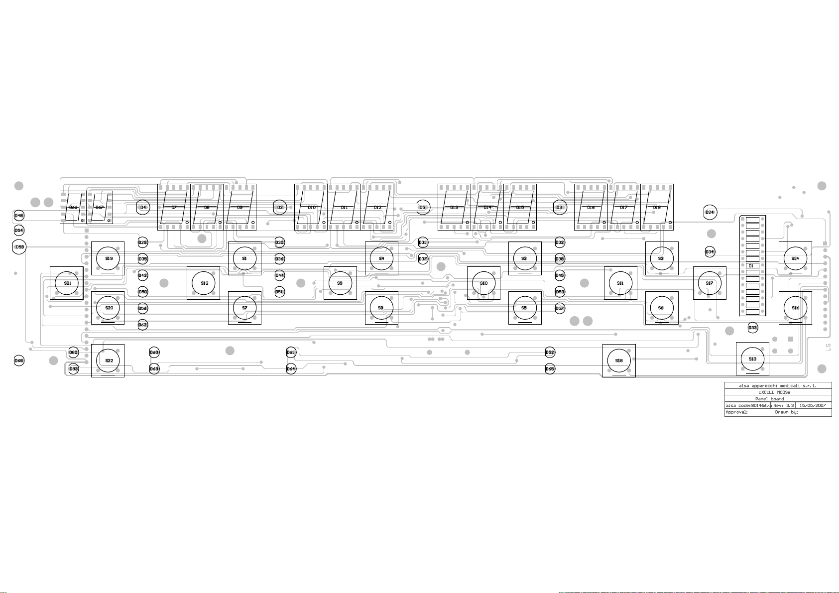
Page 46

File name: Panel board alsa code: [801466/a] Rev.: [3.3]
Date: May 15, 2007
Ref Part Type Description alsa code
__________________________________________________________________________
R1 NU NOT USED -----R2 NU NOT USED -----R3 470_SMD STANDARD CHIP RESISTOR 430499/S
R4 33_SMD STANDARD CHIP RESISTOR 430577/S
R5 NU NOT USED -----R6 33_SMD STANDARD CHIP RESISTOR 430577/S
R7 NU NOT USED -----R8 NU NOT USED -----R9 NU NOT USED -----R10 33_SMD STANDARD CHIP RESISTOR 430577/S
R11 33_SMD STANDARD CHIP RESISTOR 430577/S
R12 33_SMD STANDARD CHIP RESISTOR 430577/S
R13 33_SMD STANDARD CHIP RESISTOR 430577/S
R14 33_SMD STANDARD CHIP RESISTOR 430577/S
R15 33_SMD STANDARD CHIP RESISTOR 430577/S
R16 1K_SMD STANDARD CHIP RESISTOR 430502/S
R17 100_SMD STANDARD CHIP RESISTOR 430496/S
R18 1K_SMD STANDARD CHIP RESISTOR 430502/S
R19 100_SMD STANDARD CHIP RESISTOR 430496/S
R20 100_SMD STANDARD CHIP RESISTOR 430496/S
R21 100_SMD STANDARD CHIP RESISTOR 430496/S
R22 39K_SMD STANDARD CHIP RESISTOR 430535/S
R23 56K_SMD STANDARD CHIP RESISTOR 430522/S
C1 100n_SMD CERAMIC CHIP CAPACITOR 400320/S
C2 47U/E/35V VERTICAL ELECTROLYTIC CAPACITOR 400237
C3 100n_SMD CERAMIC CHIP CAPACITOR 400320/S
C4 100n_SMD CERAMIC CHIP CAPACITOR 400320/S
C5 1n/1%_SMD 1% CERAMIC CHIP CAPACITOR 400318/S
C6 1n/1%_SMD 1% CERAMIC CHIP CAPACITOR 400318/S
C7 100n_SMD CERAMIC CHIP CAPACITOR 400320/S
C8 22P_SMD CERAMIC CHIP CAPACITOR 400315/S
D1 LEDBAR 15GWA LEDBAR B-1500 420113
D2 GL5HB8 BLUE LED LAMP 5MM 420092
D3 GL5HB8 BLUE LED LAMP 5MM 420092
D4 GL5HY8 YELLOW LED LAMP 5MM 420036
D5 GL5HY8 YELLOW LED LAMP 5MM 420036
D6 1N4148_SMD SMD DIODE 420098/S
D7 TDSR5160 COMMON CATHODE RED 7 SEGMENT DISPLAY 420107
D8 TDSR5160 COMMON CATHODE RED 7 SEGMENT DISPLAY 420107
D9 TDSR5160 COMMON CATHODE RED 7 SEGMENT DISPLAY 420107
D10 TDSR5160 COMMON CATHODE RED 7 SEGMENT DISPLAY 420107
D11 TDSR5160 COMMON CATHODE RED 7 SEGMENT DISPLAY 420107
D12 TDSR5160 COMMON CATHODE RED 7 SEGMENT DISPLAY 420107
D13 TDSR5160 COMMON CATHODE RED 7 SEGMENT DISPLAY 420107
D14 TDSR5160 COMMON CATHODE RED 7 SEGMENT DISPLAY 420107
D15 TDSR5160 COMMON CATHODE RED 7 SEGMENT DISPLAY 420107
D16 TDSR5160 COMMON CATHODE RED 7 SEGMENT DISPLAY 420107
D17 TDSR5160 COMMON CATHODE RED 7 SEGMENT DISPLAY 420107
D18 TDSR5160 COMMON CATHODE RED 7 SEGMENT DISPLAY 420107
D19 1N4148_SMD SMD DIODE 420098/S
D20 1N4148_SMD SMD DIODE 420098/S
D21 1N4148_SMD SMD DIODE 420098/S
D22 1N4148_SMD SMD DIODE 420098/S
D23 1N4148_SMD SMD DIODE 420098/S
D24 GL5HW8 WHITE LED LAMP 5MM 420119
D25 1N4148_SMD SMD DIODE 420098/S
D26 1N4148_SMD SMD DIODE 420098/S
D27 1N4148_SMD SMD DIODE 420098/S
D28 1N4148_SMD SMD DIODE 420098/S
D29 LEDG3 GREEN LED LAMP 3MM 420079
D30 LEDG3 GREEN LED LAMP 3MM 420079
D31 LEDG3 GREEN LED LAMP 3MM 420079
D32 LEDG3 GREEN LED LAMP 3MM 420079
D33 LEDR3 RED LED LAMP 3MM 420108
D34 LEDG3 GREEN LED LAMP 3MM 420079
D35 LEDG3 GREEN LED LAMP 3MM 420079
D36 LEDG3 GREEN LED LAMP 3MM 420079
D37 LEDG3 GREEN LED LAMP 3MM 420079
D38 LEDG3 GREEN LED LAMP 3MM 420079
1
Page 47

File name: Panel board alsa code: [801466/a] Rev.: [3.3]
Date: May 15, 2007
Ref Part Type Description alsa code
__________________________________________________________________________
D39 1N4148_SMD SMD DIODE 420098/S
D40 1N4148_SMD SMD DIODE 420098/S
D41 1N4148_SMD SMD DIODE 420098/S
D42 1N4148_SMD SMD DIODE 420098/S
D43 LEDG3 GREEN LED LAMP 3MM 420079
D44 LEDG3 GREEN LED LAMP 3MM 420079
D45 LEDG3 GREEN LED LAMP 3MM 420079
D46 1N4148_SMD SMD DIODE 420098/S
D47 1N4148_SMD SMD DIODE 420098/S
D48 LEDO3 ORANGE LED LAMP 3MM 420118
D49 1N4148_SMD SMD DIODE 420098/S
D50 LEDG3 GREEN LED LAMP 3MM 420079
D51 LEDG3 GREEN LED LAMP 3MM 420079
D52 LEDG3 GREEN LED LAMP 3MM 420079
D53 LEDG3 GREEN LED LAMP 3MM 420079
D54 LEDO3 ORANGE LED LAMP 3MM 420118
D55 1N4148_SMD SMD DIODE 420098/S
D56 LEDG3 GREEN LED LAMP 3MM 420079
D57 LEDG3 GREEN LED LAMP 3MM 420079
D58 1N4148_SMD SMD DIODE 420098/S
D59 GL5HR8 RED LED LAMP 5MM 420025
D60 LEDG3 GREEN LED LAMP 3MM 420079
D61 LEDG3 GREEN LED LAMP 3MM 420079
D62 LEDG3 GREEN LED LAMP 3MM 420079
D63 LEDG3 GREEN LED LAMP 3MM 420079
D64 LEDG3 GREEN LED LAMP 3MM 420079
D65 LEDG3 GREEN LED LAMP 3MM 420079
D66 TDSL3160 COMMON CATHODE RED 7 SEGMENT DISPLAY 420096
D67 TDSL3160 COMMON CATHODE RED 7 SEGMENT DISPLAY 420096
D68 LEDR3 RED LED LAMP 3MM 420108
D69 3V9/5W ZENER DIODE 3V9/5W 420112
D70 NU NOT USED -----D71 NU NOT USED -----D72 1N4148_SMD SMD DIODE 420098/S
D73 1N4148_SMD SMD DIODE 420098/S
D74 NU NOT USED -----D75 NU NOT USED -----D76 1N4148_SMD SMD DIODE 420098/S
D77 1N4148_SMD SMD DIODE 420098/S
D78 1N4148_SMD SMD DIODE 420098/S
D79 1N4148_SMD SMD DIODE 420098/S
D80 LEDG3 GREEN LED LAMP 3MM 420079
D81 1N4148_SMD SMD DIODE 420098/S
D82 1N4148_SMD SMD DIODE 420098/S
D83 LEDG3 GREEN LED LAMP 3MM 420079
U1 MAX6954_smd SMD DISPLAY DRIVER 482118
U2 MAX6957_smd SMD DISPLAY DRIVER 482119
U3 74HCT00_SMD SMD HCT7400 482107
S1 MTG_1241 PUSHBUTTON SCHURTER 416094
S2 MTG_1241 PUSHBUTTON SCHURTER 416094
S3 MTG_1241 PUSHBUTTON SCHURTER 416094
S4 MTG_1241 PUSHBUTTON SCHURTER 416094
S5 MTG_1241 PUSHBUTTON SCHURTER 416094
S6 MTG_1241 PUSHBUTTON SCHURTER 416094
S7 MTG_1241 PUSHBUTTON SCHURTER 416094
S8 MTG_1241 PUSHBUTTON SCHURTER 416094
S9 MTG_1241 PUSHBUTTON SCHURTER 416094
S10 MTG_1241 PUSHBUTTON SCHURTER 416094
S11 MTG_1241 PUSHBUTTON SCHURTER 416094
S12 MTG_1241 PUSHBUTTON SCHURTER 416094
S13 MTG_1241 PUSHBUTTON SCHURTER 416094
S14 MTG_1241 PUSHBUTTON SCHURTER 416094
S15 NU NOT USED -----S16 MTG_1241 PUSHBUTTON SCHURTER 416094
S17 MTG_1241 PUSHBUTTON SCHURTER 416094
S18 MTG_1241 PUSHBUTTON SCHURTER 416094
S19 MTG_1241 PUSHBUTTON SCHURTER 416094
S20 MTG_1241 PUSHBUTTON SCHURTER 416094
S21 MTG_1241 PUSHBUTTON SCHURTER 416094
2
Page 48

File name: Panel board alsa code: [801466/a] Rev.: [3.3]
Date: May 15, 2007
Ref Part Type Description alsa code
__________________________________________________________________________
S22 MTG_1241 PUSHBUTTON SCHURTER 416094
J1 399030 4.8 MM FASTON CONNECTOR P.C.B. 399030
J2 CONN_21PM 21 POLES MALE CONNECTOR 384046
J3 399030 4.8 MM FASTON CONNECTOR P.C.B. 399030
J4 CONN_14PF 14 POLES FEMALE CONNECTOR 384066
3
Page 49

IIC BUS
J1
1
SDA
2
I/O
GND
3
SCL
4
GND
.
.
+5V
+15V
-15V
+5VuP
R1
CKWDT
+5V
L1
uP MASTER
POWER SUPPLY BOARDPANEL BOARD
PROGRAMMING
J11
J6
J2
1
2
3
4
5
6
7
8
9
10
11
12
13
14
J5
1
2
3
4
5
6
7
8
9
10
11
12
13
14
1
2
3
4
5
6
1
2
3
4
5
6
7
8
9
10
11
12
13
14
15
16
17
18
19
20
21
AUDALRM
VREGTST
IRFOUT
MODMEAN
SLVREQ
SLVRST
SLVBSY
SNDLV
RFBLK
GND
+15V
-15V
+24V
GND
+5V
GND
TERMPS
ALIMBLK
TERMRF
PWROFF
LEDNP
RSS232RX
RSS232TX
SLVRESET
+5V
PRMODEn
+5V
LEDNP
DYCLK
DYIKEY
DYDOUT
DYDIN
DYCS
BARCS
-15V
GND
ARGTEST
ARGPRSIN
ARGFLOW
SARGFLOW
+15V
GND
+24V
+5V
.
AN0
AN1
AN2
AN3
AN4
AN5
AN6
AN7
11
1
3
2
3
P85
+5VuP
NMIn
P86
.
P87
U5
SLVRST
+5V
DACS
ADDIN
DYCLKDAUX
R3
MANUAL
RESET
.
WDT
SLVRESET
C8
C9
C10
C11
C12
C13
C16
C19
+15V
S1
J3
D4
D5
AN_GND
R56
R61
12
R6
R8
R10
R11
AN_GND
+5V
R33
R37
R40
R43
AN_GND
D6
R57
R62
C14
R14
R15
R17
R18
R19
R20
R21
R24
.
.
12
.
C4
RESn
XT1
P10
CKWDT
DYCS
IRQ0
IRQ1
P16
P17
J12
VREF
AN_GND
C6
C7
.
AN0
AN1
AN2
AN3
AN4
AN5
AN6
AN7
AN_GND
3
2 1
U4
C1
R7
.
7
RESET
11
OSC1
10
OSC2
5
X1
4
X2
62
PB0 / AN0
61
PB1 / AN1
60
PB2 / AN2
59
PB3 / AN3
55
PB4 / AN4
56
PB5 / AN5
57
PB6 / AN6
58
PB7 / AN7
23
P1.0 / TMOW
24
P1.1
25
P1.2
51
P1.4 / IRQ0
52
P1.5 / IRQ1
53
P1.6 / IRQ2
54
P1.7 / IRQ3 / TRGV
3
AVcc
C15
TEST
R58
R60
R67
V1
+5VuP
12
6
VCL
VCC
WKP0 / P5.0
WKP1 / P5.1
WKP2 / P5.2
WKP3 / P5.3
WKP4 / P5.4
ADTRG / WKP5 / P5.5
TMRIV / P7.4
TMCIV / P7.5
TMOV / P7.6
FTCI / P8.0
FTIOA / P8.1
FTIOB / P8.2
FTIOC / P8.3
FTIOD / P8.4
SCK3 / P2.0
RXD / P2.1
TXD / P2.2
VSS
TEST
9
8
12
TEST
V2
C21
AUDALRM
J14
.
H8/3664(FP-64)_SMD
.
FQSND
Slave Microcontroller
BisMy03 micro slave.SCHDOC
alsa code: 801467
Drawn by:
D1
.
+5V
.
C3
NMI
P8.5
P8.6
P8.7
SCL
SDA
U2
35
13
14
19
20
21
22
28
29
30
36
37
38
39
40
41
42
43
44
45
46
27
26
C22
C25
NMIn
BARCS
ARGTS
SLVBY
RFSTP
SLVRQ
ARGON
DACS
TMOV
P80
P81
FTIOB
P83
P84
P85
P86
P87
DYCLK
RSS232RX
RSS232TX
SCL
SDA
R9
C5
P10
CKWDT
DYCS
J8
J10
R47
R50 +5V
.
R54
R59
.
alsa apparecchi medicali s.r.l.
EXCELL MCDSe
Rel.: 3.3 16/10/2007
R16
R26
R28
R30
R34
R38
R41
C18
3
R63
2
.
Approval:
.
+15V
6481
U3
.
C28
SDA
SCL
ARGON
DACS
P81
P80
FTIOB
P83
P84
+5V
1 2
AN_GND
5
7
.
+5V
R35
C23
R64
R66
C29
J7
.
LSO
GND
.
.
1
R12
+5V
1
GND
J13
1
2
2
3
4
5
6
7
8
9
10
2
3
4
5
6
7
8
9
10
J9
R2
R4
R5
R69
C2
D2
D3
D7
.
.
.
ADDIN
DYDIN
SLVBSY
RFBLK
ALIMBLK
SLVREQ
PWROFF
SARGFLOW
R13
DYDOUT
.
R22
NMIn
C24
.
C26
.
R23
R27
R31
R36
R42
R45
R48
R51
R52
ARGTEST
FQSND
RSS232TX
SLVBY
RFSTP
SLVRQ MODMEAN
C17
R55
R65
IRQ0
FTIOB
IRQ1DYIKEY
.
C20
.
ARGTS
TMAT
+5V
TMOV
TMAT
+5V
R68
VREGTST
IRFOUT
ARGPRSIN
ARGFLOW
TERMRF
SNDLV
TERMPS
.
.
.
C27
10
9
8
12
5
6
7
2
J4
DEBUGGER
+5V
14
4
.
VDD
R25
R29
R32
R39
R44
R46
R49
R53
U1
RS
GND
1
.
14
13
12
11
10
9
8
7
6
5
4
3
2
1
13
MCP42010_SMD
Page 50

Page 51

File name: Slave microcontroller board alsa code: [801467] Rev.: [3.3]
Date: October 16, 2007
Ref Part Type Description alsa code
__________________________________________________________________________
R1 10K_SMD STANDARD CHIP RESISTOR 430513/S
R2 47_SMD STANDARD CHIP RESISTOR 430495/S
R3 10K_SMD STANDARD CHIP RESISTOR 430513/S
R4 NU NOT USED -----R5 NU NOT USED -----R6 100_SMD STANDARD CHIP RESISTOR 430496/S
R7 15K_SMD STANDARD CHIP RESISTOR 430516/S
R8 4K7_SMD STANDARD CHIP RESISTOR 430511/S
R9 4K7_SMD STANDARD CHIP RESISTOR 430511/S
R10 100_SMD STANDARD CHIP RESISTOR 430496/S
R11 1K_SMD STANDARD CHIP RESISTOR 430502/S
R12 X_RNET10K RESISTOR NETWORK 10K 430484
R13 470_SMD STANDARD CHIP RESISTOR 430499/S
R14 5K6/1%_SMD 1% PRECISION CHIP RESISTOR 430534/S
R15 10K/1%_SMD 1% PRECISION CHIP RESISTOR 430514/S
R16 1K_SMD STANDARD CHIP RESISTOR 430502/S
R17 10K/1%_SMD 1% PRECISION CHIP RESISTOR 430514/S
R18 10K/1%_SMD 1% PRECISION CHIP RESISTOR 430514/S
R19 10K/1%_SMD 1% PRECISION CHIP RESISTOR 430514/S
R20 10K/1%_SMD 1% PRECISION CHIP RESISTOR 430514/S
R21 10K/1%_SMD 1% PRECISION CHIP RESISTOR 430514/S
R22 100_SMD STANDARD CHIP RESISTOR 430496/S
R23 100_SMD STANDARD CHIP RESISTOR 430496/S
R24 10K/1%_SMD 1% PRECISION CHIP RESISTOR 430514/S
R25 1K/1%_SMD 1% PRECISION CHIP RESISTOR 430532/S
R26 4K7_SMD STANDARD CHIP RESISTOR 430511/S
R27 100_SMD STANDARD CHIP RESISTOR 430496/S
R28 4K7_SMD STANDARD CHIP RESISTOR 430511/S
R29 1K/1%_SMD 1% PRECISION CHIP RESISTOR 430532/S
R30 4K7_SMD STANDARD CHIP RESISTOR 430511/S
R31 100_SMD STANDARD CHIP RESISTOR 430496/S
R32 1K/1%_SMD 1% PRECISION CHIP RESISTOR 430532/S
R33 10K_SMD STANDARD CHIP RESISTOR 430513/S
R34 2K2_SMD STANDARD CHIP RESISTOR 430506/S
R35 X_RNET10K RESISTOR NETWORK 10K 430484
R36 100_SMD STANDARD CHIP RESISTOR 430496/S
R37 10K_SMD STANDARD CHIP RESISTOR 430513/S
R38 10K_SMD STANDARD CHIP RESISTOR 430513/S
R39 1K/1%_SMD 1% PRECISION CHIP RESISTOR 430532/S
R40 10K_SMD STANDARD CHIP RESISTOR 430513/S
R41 2K2_SMD STANDARD CHIP RESISTOR 430506/S
R42 100_SMD STANDARD CHIP RESISTOR 430496/S
R43 10K_SMD STANDARD CHIP RESISTOR 430513/S
R44 1K/1%_SMD 1% PRECISION CHIP RESISTOR 430532/S
R45 100_SMD STANDARD CHIP RESISTOR 430496/S
R46 1K/1%_SMD 1% PRECISION CHIP RESISTOR 430532/S
R47 10K_SMD STANDARD CHIP RESISTOR 430513/S
R48 100_SMD STANDARD CHIP RESISTOR 430496/S
R49 1K/1%_SMD 1% PRECISION CHIP RESISTOR 430532/S
R50 10K_SMD STANDARD CHIP RESISTOR 430513/S
R51 100_SMD STANDARD CHIP RESISTOR 430496/S
R52 100_SMD STANDARD CHIP RESISTOR 430496/S
R53 1K/1%_SMD 1% PRECISION CHIP RESISTOR 430532/S
R54 100K_SMD STANDARD CHIP RESISTOR 430528/S
R55 100_SMD STANDARD CHIP RESISTOR 430496/S
R56 330_SMD STANDARD CHIP RESISTOR 430498/S
R57 330_SMD STANDARD CHIP RESISTOR 430498/S
R58 2K7/1%_SMD 1% PRECISION CHIP RESISTOR 430507/S
R59 22K_SMD STANDARD CHIP RESISTOR 430517/S
R60 1KT/V/10G PRESET POTENTIOMETER MULTITURN 403125
R61 330_SMD STANDARD CHIP RESISTOR 430498/S
R62 330_SMD STANDARD CHIP RESISTOR 430498/S
R63 5K6_SMD STANDARD CHIP RESISTOR 430512/S
R64 22_SMD STANDARD CHIP RESISTOR 430494/S
R65 22k_SMD STANDARD CHIP RESISTOR 430517/S
R66 22_SMD STANDARD CHIP RESISTOR 430494/S
R67 3K3/1%_SMD 1% PRECISION CHIP RESISTOR 430509/S
R68 1K_SMD STANDARD CHIP RESISTOR 430502/S
R69 NU NOT USED ------
1
Page 52

File name: Slave microcontroller board alsa code: [801467] Rev.: [3.3]
Date: October 16, 2007
Ref Part Type Description alsa code
__________________________________________________________________________
C1 100N_SMD CERAMIC CHIP CAPACITOR 400320/S
C2 100N_SMD CERAMIC CHIP CAPACITOR 400320/S
C3 10U/T/35V TANTALUM ELECTROLYTIC CAPACITOR 400134
C4 100N_SMD CERAMIC CHIP CAPACITOR 400320/S
C5 100N_SMD CERAMIC CHIP CAPACITOR 400320/S
C6 12P_SMD CERAMIC CHIP CAPACITOR 400314/S
C7 12P_SMD CERAMIC CHIP CAPACITOR 400314/S
C8 10n_SMD CERAMIC CHIP CAPACITOR 400319/S
C9 10n_SMD CERAMIC CHIP CAPACITOR 400319/S
C10 10n_SMD CERAMIC CHIP CAPACITOR 400319/S
C11 10n_SMD CERAMIC CHIP CAPACITOR 400319/S
C12 10n_SMD CERAMIC CHIP CAPACITOR 400319/S
C13 10n_SMD CERAMIC CHIP CAPACITOR 400319/S
C14 10U/T/35V TANTALUM ELECTROLYTIC CAPACITOR 400134
C15 100N_SMD CERAMIC CHIP CAPACITOR 400320/S
C16 10n_SMD CERAMIC CHIP CAPACITOR 400319/S
C17 100N_SMD CERAMIC CHIP CAPACITOR 400320/S
C18 100n_SMD CERAMIC CHIP CAPACITOR 400320/S
C19 10n_SMD CERAMIC CHIP CAPACITOR 400319/S
C20 10n_SMD CERAMIC CHIP CAPACITOR 400319/S
C21 100N_SMD CERAMIC CHIP CAPACITOR 400320/S
C22 100n_SMD CERAMIC CHIP CAPACITOR 400320/S
C23 47U/E/35V VERTICAL ELECTROLYTIC CAPACITOR 400237
C24 10n_SMD CERAMIC CHIP CAPACITOR 400319/S
C25 100n_SMD CERAMIC CHIP CAPACITOR 400320/S
C26 10n_SMD CERAMIC CHIP CAPACITOR 400319/S
C27 100n_SMD CERAMIC CHIP CAPACITOR 400320/S
C28 10n_SMD CERAMIC CHIP CAPACITOR 400319/S
C29 100n_SMD CERAMIC CHIP CAPACITOR 400320/S
D1 5V6/5W ZENER DIODE 5.6V/5W (1N5339) 420088
D2 NU NOT USED -----D3 NU NOT USED -----D4 LS101A_SMD SMD SCHOTTKY DIODE 420111/S
D5 LS101A_SMD SMD SCHOTTKY DIODE 420111/S
D6 5V1_SMD SMD ZENER DIODE 420101/S
D7 NU NOT USED -----U1 TC32M WATCHDOG TIMER 482105
U2 H8/3664_SMD 16-BIT MICROCONTROLLER 482121
U3 LM386_SMD SMD BF LM386 482104
U4 LM431 VOLTAGE REGULATOR 482078
U5 MCP42010_SMD SMD DIGITAL POTENTIOMETER 482120
L1 6uH8/800mA INDUCTOR 422007
XT1 16MHZ/HC18 QUARTZ CRYSTAL 16 MHZ 252012
S1 NU NOT USED -----J1 PICO_4 4 POLES PICOFLEX CONN. MALE P.C.B. 384042
J2 PICO_14 14 POLES PICOFLEX CONN. MALE P.C.B. 384040
J3 CONN_2PM 2 POLES MALE CONNECTOR 384052
J4 NU NOT USED -----J5 PICO_14 14 POLES PICOFLEX CONN. MALE P.C.B. 384040
J6 PICO_6 6 POLES PICOFLEX CONN. MALE P.C.B. 384048
J7 399030 4.8 MM FASTON CONNECTOR P.C.B. 399030
J9 NU NOT USED -----J11 CONN_21PF 21 POLES FEMALE CONNECTOR 384047
J12 CONN_2P_B 2 POLES MALE CONNECTOR 384052
J13 CONN_2P_AMP 2 POLES MALE CONNECTOR 384068
J14 CONN_2P_B 2 POLES MALE CONNECTOR 384052
2
Page 53

+24V
+24V
+5V
+15V
+24V
D2
D4
R2
VARGGEV VARGTEST
R4
SARGFLOW ARGTEST
C13
. .
J1
4
3
2
1
R9
R15
+5V
3
VCC
2
GND
.
C7
C11
.
Q4
. .
S1
1
OUT+
R30
J7
R38
R43
+15V
R8
R37
R44
Q2
R11
..
R21
.
C8
.
+Vref
D11
D12
.
.
R18
R26
+Vref
C9
U2
C1
R5
R13
.
2 1
.
D5
..
C3
R19
5
6
R22
R27
.
R33
3
R42
R40
U1B
R24
7
.
.
R34
R28
C14
R48
R39
+Vref
R20
D1
D3
+15V+15V
R3
R10
R16
R23
.
.
.
C6
-15V
R41
R29
R32
Q3
. .
C4
.
+15V
3
2
R7
+5V
84
U1A
.
Q1
R12
D7
ARGPRSIN
D8
.
C5
.
1
R35
C12
.
R31
R1
C2
R14
. .
R17
J2
R25
R36
.
.
R6
D6
+Vref
.
C10
ARGCILPRS
+5V
D9
ARGFLOW
D10
.
V1
J3
EXCELL MCDSe
Argon management board
V2
alsa apparecchi medicali s.r.l.
R45 R46
D14D13
. .
J4
1
+24V
VARGGEV
2
3
+24V
4
VARGTEST
5
TO SOLENOID VALVES
J5
1
+15V
2
GND
3
+24V
4
ARGTEST
5
-15V
6
ARGPRSIN
ARGFLOW
7
8
ARGCILPRS
9
10
SARGFLOW
11
TO PANEL BOARD
12
+5V
13
14
GND
J6
R47
D15
.
. .
.
C15
C16
Bismy03 Argon.Schdoc
alsa code: 801468
Drawn by:
Rel.: 2.2 15/05/2007
Approval:
Page 54

Page 55

File name: Argon management board alsa code: [801468] Rev.: [2.2]
Date: May 15, 2007
Ref. Part Type Description alsa code
__________________________________________________________________________
R1 4K7_SMD STANDARD CHIP RESISTOR 430511/S
R2 4K7_SMD STANDARD CHIP RESISTOR 430511/S
R3 4K7_SMD STANDARD CHIP RESISTOR 430511/S
R4 4K7_SMD STANDARD CHIP RESISTOR 430511/S
R5 15K METAL FILM RESISTOR 1/4 W 5% 430345
R6 15K METAL FILM RESISTOR 1/4 W 5% 430345
R7 100_SMD STANDARD CHIP RESISTOR 430496/S
R8 100_SMD STANDARD CHIP RESISTOR 430496/S
R9 10K_SMD STANDARD CHIP RESISTOR 430513/S
R10 10K_SMD STANDARD CHIP RESISTOR 430513/S
R11 2K2_SMD STANDARD CHIP RESISTOR 430506/S
R12 2K2_SMD STANDARD CHIP RESISTOR 430506/S
R13 100/1W METAL FILM RESISTOR 1 W 430008
R14 100/1W METAL FILM RESISTOR 1 W 430008
R15 47K_SMD STANDARD CHIP RESISTOR 430520/S
R16 47K_SMD STANDARD CHIP RESISTOR 430520/S
R17 10K_SMD STANDARD CHIP RESISTOR 430513/S
R18 470_SMD STANDARD CHIP RESISTOR 430499/S
R19 470_SMD STANDARD CHIP RESISTOR 430499/S
R20 470_SMD STANDARD CHIP RESISTOR 430499/S
R21 5K6_SMD STANDARD CHIP RESISTOR 430512/S
R22 10K_SMD STANDARD CHIP RESISTOR 430513/S
R23 22K_SMD STANDARD CHIP RESISTOR 430517/S
R24 1K5_SMD STANDARD CHIP RESISTOR 430503/S
R25 NU NOT USED -----R26 5KT/6mm MINIATURE TRIMMER 403113/S
R27 5K6_SMD STANDARD CHIP RESISTOR 430512/S
R28 470_SMD STANDARD CHIP RESISTOR 430499/S
R29 470_SMD STANDARD CHIP RESISTOR 430499/S
R30 100_SMD STANDARD CHIP RESISTOR 430496/S
R31 470_SMD STANDARD CHIP RESISTOR 430499/S
R32 10K_SMD STANDARD CHIP RESISTOR 430513/S
R33 8K/1%_SMD PRECISION RESISTOR 1% 430563/S
R34 5K6_SMD STANDARD CHIP RESISTOR 430512/S
R35 1K5_SMD STANDARD CHIP RESISTOR 430503/S
R36 22K_SMD STANDARD CHIP RESISTOR 430517/S
R37 100_SMD STANDARD CHIP RESISTOR 430496/S
R38 100_SMD STANDARD CHIP RESISTOR 430496/S
R39 5KT/6mm MINIATURE TRIMMER 403113/S
R40 2KT/6mm MINIATURE TRIMMER 403112/S
R41 5K6_SMD STANDARD CHIP RESISTOR 430512/S
R42 3K/1%_SMD PRECISION RESISTOR 1% 430533/S
R43 100_SMD STANDARD CHIP RESISTOR 430496/S
R44 100_SMD STANDARD CHIP RESISTOR 430496/S
R45 NU NOT USED -----R46 NU NOT USED -----R47 NU NOT USED -----R48 100_SMD STANDARD CHIP RESISTOR 430496/S
C1 100N/P/100V METALLIZED FILM CAPACITOR 400313
C2 100N/P/100V METALLIZED FILM CAPACITOR 400313
C3 100N_SMD CERAMIC CHIP CAPACITOR 400320/S
C4 10N_SMD CERAMIC CHIP CAPACITOR 400319/S
C5 100N_SMD CERAMIC CHIP CAPACITOR 400320/S
C6 100N_SMD CERAMIC CHIP CAPACITOR 400320/S
C7 100N_SMD CERAMIC CHIP CAPACITOR 400320/S
C8 100N_SMD CERAMIC CHIP CAPACITOR 400320/S
C9 10U/T/35V TANTALUM ELECTROLYTIC CAPACITOR 400134
C10 10N_SMD CERAMIC CHIP CAPACITOR 400319/S
C11 100N_SMD CERAMIC CHIP CAPACITOR 400320/S
C12 100N_SMD CERAMIC CHIP CAPACITOR 400320/S
C13 10U/T/35V TANTALUM ELECTROLYTIC CAPACITOR 400134
C14 1U/T/35V TANTALUM ELECTROLYTIC CAPACITOR 400173
C15 10U/T/35V TANTALUM ELECTROLYTIC CAPACITOR 400134
C16 100N_SMD CERAMIC CHIP CAPACITOR 400320/S
D3 1N4007 DIODE 420001
D4 1N4007 DIODE 420001
D5 1N4007 DIODE 420001
D6 1N4007 DIODE 420001
D7 LS101A_SMD SMD SCHOTTKY DIODE 420111/S
1
Page 56

File name: Argon management board alsa code: [801468] Rev.: [2.2]
Date: May 15, 2007
Ref. Part Type Description alsa code
__________________________________________________________________________
D8 LS101A_SMD SMD SCHOTTKY DIODE 420111/S
D9 LS101A_SMD SMD SCHOTTKY DIODE 420111/S
D10 LS101A_SMD SMD SCHOTTKY DIODE 420111/S
D11 5V1_SMD SMD ZENER DIODE 420101/S
D12 5V1_SMD SMD ZENER DIODE 420101/S
D13 NU NOT USED -----D14 NU NOT USED -----D15 NU NOT USED -----Q1 IRF540 N CHANNEL MOSFET 427079
Q2 IRF540 N CHANNEL MOSFET 427079
Q3 BC817_SMD SMD NPN TRANSISTOR 427089/S
Q4 BC817_SMD SMD NPN TRANSISTOR 427089/S
U1 TL072_SMD SMD OP.AMP. TL072 482125
U2 LM431 VOLTAGE REGULATOR 482078
S1 MPX5700 ABSOLUTE PRESSURE SENSOR 482110
J1 CONN_4P_AMP 4 POLES MALE CONNECTOR 384061
J4 384016 5 POLES PCB CONNECTOR MASCON 384016
J5 CONN_14PM 14 POLES MALE CONNECTOR 384065
J6 399030 4.8 MM FASTON CONNECTOR P.C.B. 399030
2
Page 57

To HF READER SECTION
To SLAVE uC
To POWER SUPPLY BOARD
To MOTHER BOARD
J2
J9
.
.
1
2
3
4
5
6
J4
1
2
3
4
J5
1
2
3
4
5
6
7
8
9
10
11
12
13
14
J8
1
2
3
4
1
2
3
4
5
6
J12
1
2
3
4
5
6
7
8
9
10
11
12
13
14
SDA
SCL
INTIIA
SNUBB
SNDLV
AUBIPLV
GND
VOUTPK
IMOSPK
GND
VLOG
PHASE
ILOG
VLOGAIN
ENMONBIP
AGND
SDA
SCL
.
AUDALRM
VREGTST
IRFOUT
MODMEAN
SLVREQ
SLVRST
SLVBSY
SNDLV
RFBLK
GND
SDA
SCL
.
RSM232RX
GND
RSM232TX
MSTRESET
+5V
PRMODE
+15V
GND
-15V
GND
+5V
GND
INTIIA
PWRAUD
ENALIM
REMLEV
PWROFF
J20
1
3
5
7
9
11
13
15
17
19
21
23
25
R24
.
.
.
RXD0
C5
C8
C10
11
TXD0
R113
R126
R134
CIN0
CIN5
CIN2
P26/A14/PW14
P25/A13/PW13
P24/A12/PW12
P23/A11/PW11
P22/A10/PW10
P21/A9/PW9
P20/A8/PW8
P17/A7/PW7
P16/A6/PW6
P15/A5/PW5
P14/A4/PW4
P13/A3/PW3
P12/A2/PW2
P11/A1/PW1
P10/A0/PW0
P37/D7/HDB7
P36/D6/HDB6
P35/D5/HDB5
P34/D4/HDB4
P33/D3/HDB3
P32/D2/HDB2
P31/D1/HDB1
P30/D0/HDB0
+5V
R114
VDD
R131
C1
C2
C3
+5V
.
D1
C6
C7
47
8
VCL
VCC1
U3
RFOLL
BATT
D9
INT7OSCI
6
SCL
5
SDA
J1
GND
.
.
.
.
C13
.
P27
48
P26
49
P25
50
P24
51
P23
52
P22
53
54
FRQ1
PWAU
55
ENAL
57
58
ENMB
59
SFUN
60
RFEN
61
GVLG
EBAU
62
WPEE
63
P10
64
72
P37
71
P36
70
P35
69
P34
68
P33
67
P32
66
P31
65
P30
.
+15V
C32
U4
1
8
R121
7
6
5
4
.
B1
.
C41
.
8
1
VDT
3
A0
2
OSCO
VSS
4
U7
.
2
R93
R98
R100
.
+5V
R16 R17
. .
+5V
C42
+15V
R39
R42
R44
R46
R48
R51
R53
R54
R56
R59
R61
R63
R65
R69
R72
R74
R76
R78
R81
R82
R84
DRIVRF
XT2
D3D2
D6
-15V
+5V
.
R18
D4
.
D5
MODMEAN
C38
.
C14
20
+5V
VCC
TMOX
4
TMOX
RFEN
6
RFENBL
TMO1
5
TMO1
TMO0
3
TMO0
SFUN
2
SELFUN
RFDSBL
7
RFBLK
8
MD1
PRMODE
WDT
9
WDT
10
GND
.
C18
C19
IRQ1 SL VREQ
IRQ6 INTIIA
C20
R79
SLVR SLVRST
R83
EBAU
R86
FRQ1
R88
PWAU
R91
PWX0
R96
PWX1
R99
ENMB
R101
GVLG VLOGAIN
R103
ENAL
R116
CIN2 MODMEAN
R117
CIN5
R118
CIN0
R120
AN7
R122
AN6
R123
AN5
R124
AN4
R127
AN3
R129
AN2
R132
AN1
R135
AN0
V1
V2
V3
Master Microcontroller Board
V4
Bismy03MicroMaster.SchDoc
alsa code: 801469
Drawn by: Gianni Rocca
AUDALRM
C12
U2
AUDAL
EAUD
RFOUT
TMOXBUF
SNUB
RESn
R57
R62
R66
R70
ENBIPAUT
BTMHND
PWRAUD
SVOUTPK
SIMOSPK
ENMONBIP
ENALIM
REMLEV
AUBIPLV
IRFOUT
IRFLEAK
VREGTST
PHASE
ILOG
VLOG
VOUTPK
IMOSPK
R31
R34
15
11
12
R40
13
R45
14
R49
19
R52
RFBLKRFDSBL
SLVBSYC21.SLVBY
C22
C23
.
C35
C37
C39
.
alsa apparecchi medicali s.r.l.
EXCELL MCDSe
Rel. 2.2 15/05/2007
Approval:
+5V
EAL2
RFOLL
+5V
R35
R38
TMRI1
TMCI1
+5V
SNUBB
RES_GL
+5V
C11
29
+5V
AVCC
C33
D8
R125
.
R20
RESn
1
RES
AVSS
38
AVSS
J16
.
1
A0
A12SCL
3
A2
SCLSCK1
80
R1R2R3R4R5R6R7
P81
SLVR
EAL2
TXD1
RXD1
75
76
78
79
77
P83
P82/HIFSD
P81/CS2/GA20
P84/IRQ3/TxD1
P85/IRQ4/RxD1
P86/IRQ5/SCK1/SCL1
VSS
VSS
VSS
12
56
73
.
I2C BUS
SELECTION
WRITE
PROT.
+5V
2
U6
8
7
WP
VDD
6
5
SDA
VSS
4
.
CKWDT
74
P80/HA0
J21
1
R128
R130
R133
R12
TMOX
28
P67/TMOX/CIN7/KIN7/IRQ7
46
PWX1
R104
+5V
R13
IRQ6
27
P66/FTOB/CIN6/KIN6/IRQ6
PWX0
R105
+5V
+5V
R19
MD1
R25
.
PRMODE
MSTRESET
C16
.
.
R85
RXD1
R87
TXD1
+15V
.
.
.
R119
IRQ0
C40
.
2
IRFLEAK
4
6
GND
ENBIPAUT
8
IRFOUT
10
GND
12
14
16
SVOUTPK
18
SIMOSPK
20
22
24
VREGTST
26
DRIVRF
R28R27
.
C9
.
R33R32
RES_GL
+5V
R41
R43
R47
R50
R55
R58
R60
R64
R67
R68
R71
R73
R75
R77
R80
AVSS
R89
R94
.
.
C4
Q1
R29
.
R30
Q2
.
C24 C25 C26 C27 C28 C29 C30 C31
R90
R95
C34
AVSS
AVSS
RESn
.
2 1
S1
U5
2
VDD
AVSS
3
R92
R115
R15
U1
3
RS
GND
1
.
C15
.
C17
R36
.
VREF
R102
VSS
R37
R97
AVSS
CKWDT
R22R21
2
J3
XT1
SDA0
P96
SLVBY
WRn
RDn
IRQ0
IRQ1
P90
AN7
AN6
AN5
AN4
AN3
AN2
AN1
AN0
C36
+5VVDD
.
1
MD1
MD0
NMIn
STBYn
C43
J10
1
J11
AGND
+5V
R23
R26
WDT
.
2
XTAL
3
EXTAL
4
MD1
5
MD0
6
NMI
7
STBY
13
P97/WAIT/SDA0
14
P96/PHI/EXCL
15
P95/AS/IOS/CS1
16
P94/WR/IOW
17
P93/IOR/RD
18
P92/IRQ0
19
P91/IRQ1
20
P90/IRQ2/ADTRG/ECS2
37
P77/AN7/DA1
36
P76/AN6/DA0
35
P75/AN5
34
P74/AN4
33
P73/AN3
32
P72/AN2
31
P71/AN1
30
P70/AN0
2
D7
AVSS
J13
R136
AVSS
1
2
J24
R14
CIN5
26
P65/FTID/CIN5/KIN5
P45/TMRI1/HIRQ12/CSYNCI44P46/PWX045P47/PWX1
TMRI1
R106
SDA1
132
J19
WPEE
SCL
SDA
P64
25
P64/FTIC/CIN4/KIN4/CLAMPO
43
TMO1
SDA
R107
R8
V5TEST
24
P63/FTIB/CIN3/KIN3/VFBACKI
TMCI1
R108
SDA0
R9
CIN2
23
P62/FTIA/CIN2/KIN2/TMIY/VSYNCI
SDA1
R109
R11
R10
.
CIN0
FTOA
21
22
P27/A15/PW15/CBLANK
P61/FTOA/CIN1/KIN1/VSYNCO
P60/FTCI/CIN0/KIN0/TMIX/HFBACKI
P52/SCK0/SCL09P51/RxD010P50/TxD0
P40/TMCI0/TxD2/IrTxD39P41/TMO0/RxD2/IrRxD40P42/TMRI0/SCK2/SDA141P43/TMCI1/HIRQ11/HSYNCI42P44/TMO1/HIRQ1/HSYNCO
TMO0
SCL0
P40
R110
R111
R112
SCLSCK1
SCL0
SCL
132
J18
J23
RTCK
SCL
SDA
Page 58

Page 59

File name: Master microcontroller board alsa code: [801469] Rev.: [2.2]
Date: May 15, 2007
Ref Part Type Description alsa code
__________________________________________________________________________
R1 10K_SMD STANDARD CHIP RESISTOR 430513/S
R2 10K_SMD STANDARD CHIP RESISTOR 430513/S
R3 10K_SMD STANDARD CHIP RESISTOR 430513/S
R4 10K_SMD STANDARD CHIP RESISTOR 430513/S
R5 10K_SMD STANDARD CHIP RESISTOR 430513/S
R6 10K_SMD STANDARD CHIP RESISTOR 430513/S
R7 10K_SMD STANDARD CHIP RESISTOR 430513/S
R8 3K3/1%_SMD 1% PRECISION CHIP RESISTOR 430509/S
R9 10K/1%_SMD 1% PRECISION CHIP RESISTOR 430514/S
R10 10K_SMD STANDARD CHIP RESISTOR 430513/S
R11 10K/1%_SMD 1% PRECISION CHIP RESISTOR 430514/S
R12 10K_SMD STANDARD CHIP RESISTOR 430513/S
R13 10K_SMD STANDARD CHIP RESISTOR 430513/S
R14 10K/1%_SMD 1% PRECISION CHIP RESISTOR 430514/S
R15 10K_SMD STANDARD CHIP RESISTOR 430513/S
R16 NU NOT USED -----R17 NU NOT USED -----R18 NU NOT USED -----R19 10K_SMD STANDARD CHIP RESISTOR 430513/S
R20 15K_SMD STANDARD CHIP RESISTOR 430516/S
R21 47_SMD STANDARD CHIP RESISTOR 430495/S
R22 10K_SMD STANDARD CHIP RESISTOR 430513/S
R23 10K_SMD STANDARD CHIP RESISTOR 430513/S
R24 3K3/1%_SMD 1% PRECISION CHIP RESISTOR 430509/S
R25 47K_SMD STANDARD CHIP RESISTOR 430520/S
R26 220_SMD STANDARD CHIP RESISTOR 430497/S
R27 10K_SMD STANDARD CHIP RESISTOR 430513/S
R28 10K_SMD STANDARD CHIP RESISTOR 430513/S
R29 47K_SMD STANDARD CHIP RESISTOR 430520/S
R30 1K_SMD STANDARD CHIP RESISTOR 430502/S
R31 22K_SMD STANDARD CHIP RESISTOR 430517/S
R32 10K_SMD STANDARD CHIP RESISTOR 430513/S
R33 10K_SMD STANDARD CHIP RESISTOR 430513/S
R34 2K2_SMD STANDARD CHIP RESISTOR 430506/S
R35 2k2_SMD STANDARD CHIP RESISTOR 430506/S
R36 100_SMD STANDARD CHIP RESISTOR 430496/S
R37 10K_SMD STANDARD CHIP RESISTOR 430513/S
R38 100_SMD STANDARD CHIP RESISTOR 430496/S
R39 10K_SMD STANDARD CHIP RESISTOR 430513/S
R40 100_SMD STANDARD CHIP RESISTOR 430496/S
R41 10K_SMD STANDARD CHIP RESISTOR 430513/S
R42 10K_SMD STANDARD CHIP RESISTOR 430513/S
R43 10K_SMD STANDARD CHIP RESISTOR 430513/S
R44 10K_SMD STANDARD CHIP RESISTOR 430513/S
R45 2K2_SMD STANDARD CHIP RESISTOR 430506/S
R46 10K_SMD STANDARD CHIP RESISTOR 430513/S
R47 10K_SMD STANDARD CHIP RESISTOR 430513/S
R48 10K_SMD STANDARD CHIP RESISTOR 430513/S
R49 100_SMD STANDARD CHIP RESISTOR 430496/S
R50 10K_SMD STANDARD CHIP RESISTOR 430513/S
R51 10K_SMD STANDARD CHIP RESISTOR 430513/S
R52 1K_SMD STANDARD CHIP RESISTOR 430502/S
R53 10K_SMD STANDARD CHIP RESISTOR 430513/S
R54 10K_SMD STANDARD CHIP RESISTOR 430513/S
R55 10K_SMD STANDARD CHIP RESISTOR 430513/S
R56 10K_SMD STANDARD CHIP RESISTOR 430513/S
R57 100_SMD STANDARD CHIP RESISTOR 430496/S
R58 10K_SMD STANDARD CHIP RESISTOR 430513/S
R59 10K_SMD STANDARD CHIP RESISTOR 430513/S
R60 10K_SMD STANDARD CHIP RESISTOR 430513/S
R61 10K_SMD STANDARD CHIP RESISTOR 430513/S
R62 220_SMD STANDARD CHIP RESISTOR 430497/S
R63 10K_SMD STANDARD CHIP RESISTOR 430513/S
R64 10K/1%_SMD 1% PRECISION CHIP RESISTOR 430514/S
R65 10K_SMD STANDARD CHIP RESISTOR 430513/S
R66 220_SMD STANDARD CHIP RESISTOR 430497/S
R67 10K/1%_SMD 1% PRECISION CHIP RESISTOR 430514/S
R68 10K/1%_SMD 1% PRECISION CHIP RESISTOR 430514/S
R69 10K_SMD STANDARD CHIP RESISTOR 430513/S
1
Page 60

File name: Master microcontroller board alsa code: [801469] Rev.: [2.2]
Date: May 15, 2007
Ref Part Type Description alsa code
__________________________________________________________________________
R70 220_SMD STANDARD CHIP RESISTOR 430497/S
R71 10K/1%_SMD 1% PRECISION CHIP RESISTOR 430514/S
R72 10K_SMD STANDARD CHIP RESISTOR 430513/S
R73 10K/1%_SMD 1% PRECISION CHIP RESISTOR 430514/S
R74 10K_SMD STANDARD CHIP RESISTOR 430513/S
R75 10K/1%_SMD 1% PRECISION CHIP RESISTOR 430514/S
R76 10K_SMD STANDARD CHIP RESISTOR 430513/S
R77 1K/1%_SMD 1% PRECISION CHIP RESISTOR 430532/S
R78 10K_SMD STANDARD CHIP RESISTOR 430513/S
R79 220_SMD STANDARD CHIP RESISTOR 430497/S
R80 1K/1%_SMD 1% PRECISION CHIP RESISTOR 430532/S
R81 10K_SMD STANDARD CHIP RESISTOR 430513/S
R82 10K_SMD STANDARD CHIP RESISTOR 430513/S
R83 220_SMD STANDARD CHIP RESISTOR 430497/S
R84 10K_SMD STANDARD CHIP RESISTOR 430513/S
R85 100_SMD STANDARD CHIP RESISTOR 430496/S
R86 100_SMD STANDARD CHIP RESISTOR 430496/S
R87 100_SMD STANDARD CHIP RESISTOR 430496/S
R88 100_SMD STANDARD CHIP RESISTOR 430496/S
R89 330_SMD STANDARD CHIP RESISTOR 430498/S
R90 330_SMD STANDARD CHIP RESISTOR 430498/S
R91 100_SMD STANDARD CHIP RESISTOR 430496/S
R92 100_SMD STANDARD CHIP RESISTOR 430496/S
R93 47_SMD STANDARD CHIP RESISTOR 430495/S
R94 330_SMD STANDARD CHIP RESISTOR 430498/S
R95 330_SMD STANDARD CHIP RESISTOR 430498/S
R96 100_SMD STANDARD CHIP RESISTOR 430496/S
R97 2K7/1%_SMD 1% PRECISION CHIP RESISTOR 430507/S
R98 220_SMD STANDARD CHIP RESISTOR 430497/S
R99 1K_SMD STANDARD CHIP RESISTOR 430502/S
R100 8K2/1%_SMD 1% PRECISION CHIP RESISTOR 430539/S
R101 1K_SMD STANDARD CHIP RESISTOR 430502/S
R102 1KT PRESET POTENTIOMETER CERMET 403063
R103 1K_SMD STANDARD CHIP RESISTOR 430502/S
R104 10K_SMD STANDARD CHIP RESISTOR 430513/S
R105 10K_SMD STANDARD CHIP RESISTOR 430513/S
R106 10K_SMD STANDARD CHIP RESISTOR 430513/S
R107 10K_SMD STANDARD CHIP RESISTOR 430513/S
R108 10K_SMD STANDARD CHIP RESISTOR 430513/S
R109 10K_SMD STANDARD CHIP RESISTOR 430513/S
R110 10K_SMD STANDARD CHIP RESISTOR 430513/S
R111 10K_SMD STANDARD CHIP RESISTOR 430513/S
R112 10K_SMD STANDARD CHIP RESISTOR 430513/S
R113 10K_SMD STANDARD CHIP RESISTOR 430513/S
R114 10K_SMD STANDARD CHIP RESISTOR 430513/S
R115 3K3/1%_SMD 1% PRECISION CHIP RESISTOR 430509/S
R116 1K/1%_SMD 1% PRECISION CHIP RESISTOR 430532/S
R117 1K_SMD STANDARD CHIP RESISTOR 430502/S
R118 1K_SMD STANDARD CHIP RESISTOR 430502/S
R119 220_SMD STANDARD CHIP RESISTOR 430497/S
R120 1K/1%_SMD 1% PRECISION CHIP RESISTOR 430532/S
R121 NU NOT USED -----R122 1K/1%_SMD 1% PRECISION CHIP RESISTOR 430532/S
R123 1K/1%_SMD 1% PRECISION CHIP RESISTOR 430532/S
R124 1K/1%_SMD 1% PRECISION CHIP RESISTOR 430532/S
R125 10k_SMD STANDARD CHIP RESISTOR 430513/S
R126 NU NOT USED -----R127 1K/1%_SMD 1% PRECISION CHIP RESISTOR 430532/S
R128 220_SMD STANDARD CHIP RESISTOR 430497/S
R129 1k/1%_SMD 1% PRECISION CHIP RESISTOR 430532/S
R130 220_SMD STANDARD CHIP RESISTOR 430497/S
R131 NU NOT USED -----R132 1K/1%_SMD 1% PRECISION CHIP RESISTOR 430532/S
R133 220_SMD STANDARD CHIP RESISTOR 430497/S
R134 NU NOT USED -----R135 1K/1%_SMD 1% PRECISION CHIP RESISTOR 430532/S
R136 0/0 0 OHM RESISTOR 430446
C1 10n_SMD CERAMIC CHIP CAPACITOR 400319/S
C2 10n_SMD CERAMIC CHIP CAPACITOR 400319/S
2
Page 61

File name: Master microcontroller board alsa code: [801469] Rev.: [2.2]
Date: May 15, 2007
Ref Part Type Description alsa code
__________________________________________________________________________
C3 10n_SMD CERAMIC CHIP CAPACITOR 400319/S
C4 100N_SMD CERAMIC CHIP CAPACITOR 400320/S
C5 22U/E/100V/V VERTICAL ELECTROLYTIC CAPACITOR SMPS 400286
C6 100N_SMD CERAMIC CHIP CAPACITOR 400320/S
C7 100N_SMD CERAMIC CHIP CAPACITOR 400320/S
C8 10U/T/35V TANTALUM ELECTROLYTIC CAPACITOR 400134
C9 100n_SMD CERAMIC CHIP CAPACITOR 400320/S
C10 100n_SMD CERAMIC CHIP CAPACITOR 400320/S
C11 100n_SMD CERAMIC CHIP CAPACITOR 400320/S
C12 100n_SMD CERAMIC CHIP CAPACITOR 400320/S
C13 100n_SMD CERAMIC CHIP CAPACITOR 400320/S
C14 100n_SMD CERAMIC CHIP CAPACITOR 400320/S
C15 33p_SMD CERAMIC CHIP CAPACITOR 400334/S
C16 100n_SMD CERAMIC CHIP CAPACITOR 400320/S
C17 33p_SMD CERAMIC CHIP CAPACITOR 400334/S
C18 10n_SMD CERAMIC CHIP CAPACITOR 400319/S
C19 10n_SMD CERAMIC CHIP CAPACITOR 400319/S
C20 10n_SMD CERAMIC CHIP CAPACITOR 400319/S
C21 10n_SMD CERAMIC CHIP CAPACITOR 400319/S
C22 10n_SMD CERAMIC CHIP CAPACITOR 400319/S
C23 10n_SMD CERAMIC CHIP CAPACITOR 400319/S
C24 10n_SMD CERAMIC CHIP CAPACITOR 400319/S
C25 10n_SMD CERAMIC CHIP CAPACITOR 400319/S
C26 10n_SMD CERAMIC CHIP CAPACITOR 400319/S
C27 10n_SMD CERAMIC CHIP CAPACITOR 400319/S
C28 10n_SMD CERAMIC CHIP CAPACITOR 400319/S
C29 10n_SMD CERAMIC CHIP CAPACITOR 400319/S
C30 10n_SMD CERAMIC CHIP CAPACITOR 400319/S
C31 10n_SMD CERAMIC CHIP CAPACITOR 400319/S
C32 100n_SMD CERAMIC CHIP CAPACITOR 400320/S
C33 100N_SMD CERAMIC CHIP CAPACITOR 400320/S
C34 100n_SMD CERAMIC CHIP CAPACITOR 400320/S
C35 10n_SMD CERAMIC CHIP CAPACITOR 400319/S
C36 10U/T/35V TANTALUM ELECTROLYTIC CAPACITOR 400134
C37 10n_SMD CERAMIC CHIP CAPACITOR 400319/S
C38 100n_SMD CERAMIC CHIP CAPACITOR 400320/S
C39 10n_SMD CERAMIC CHIP CAPACITOR 400319/S
C40 10N_SMD CERAMIC CHIP CAPACITOR 400319/S
C41 NU NOT USED -----C42 NU NOT USED -----C43 100n_SMD CERAMIC CHIP CAPACITOR 400320/S
D1 5V6/5W ZENER DIODE 5.6V/5W (1N5339) 420088
D2 NU NOT USED -----D3 NU NOT USED -----D4 NU NOT USED -----D5 LS101A_SMD SMD SCHOTTKY DIODE 420111/S
D6 LS101A_SMD SMD SCHOTTKY DIODE 420111/S
D7 5V1_SMD SMD ZENER DIODE 420101/S
D8 5V1_SMD SMD ZENER DIODE 420101/S
D9 NU NOT USED -----Q1 BC817_SMD SMD NPN TRANSISTOR 427089/S
Q2 BC817_SMD SMD NPN TRANSISTOR 427089/S
U1 TC32M WATCHDOG TIMER 482105
U2 GAL_BIS7 GAL 16V8 FOR NHP-MCDSE 714243
U3 HD64F2138_SMD 16/32-BIT MICROCONTROLLER 482137
U4 MIC4451_SMD SMD INVERTING MOSFET DRIVER 482122
U5 LM431 VOLTAGE REGULATOR 482078
U6 24C256 CMOS SERIAL EEPROM 482138
U7 NU NOT USED -----XT1 20MHZ/HC18 QUARTZ CRYSTAL 20 MHZ 252013
XT2 NU NOT USED -----S1 NU NOT USED -----J1 399030 4.8 MM FASTON CONNECTOR P.C.B. 399030
J2 PICO_6 6 POLES PICOFLEX CONN. MALE P.C.B. 384048
J3 CONN_2PM 2 POLES MALE CONNECTOR 384052
J4 NU NOT USED -----J5 PICO_14 14 POLES PICOFLEX CONN. MALE P.C.B. 384040
J8 PICO_4 4 POLES PICOFLEX CONN. MALE P.C.B. 384042
J9 PICO_6 6 POLES PICOFLEX CONN. MALE P.C.B. 384048
3
Page 62

File name: Master microcontroller board alsa code: [801469] Rev.: [2.2]
Date: May 15, 2007
Ref Part Type Description alsa code
__________________________________________________________________________
J11 CONN_2PM 2 POLES MALE CONNECTOR 384052
J12 PICO_14 14 POLES PICOFLEX CONN. MALE P.C.B. 384040
J13 399030 4.8 MM FASTON CONNECTOR P.C.B. 399030
J16 399030 4.8 MM FASTON CONNECTOR P.C.B. 399030
J18 conn_3p_b 3 POLES MALE CONNECTOR 384069
J19 conn_3p_b 3 POLES MALE CONNECTOR 384069
J20 PICO_26 26 POLES PICOFLEX CONN. MALE P.C.B. 384044
J21 NU NOT USED -----J24 CONN_2PM 2 POLES MALE CONNECTOR 384052
4
Page 63

+15V
R1
15
+VIN
SS
8
Q5
R59
100K
470u/E/250V
R74
150K
RSS232RX
GND
RSS232TX
SLVRESET
+5V
PRMODEn
+15V
-15V
+24V
GND
+5V
GND
TERMPS
ALIMBLK
TERMRF
PWROFF
LEDNP
SDA
SCL
R2
22
UC3525_SMD
R50
100
100
R51
C51
NS
NS
R80
47K
C68
100n
LS101A_SMD
22
13
VC
SHUNT
C44
1n
OUT A
OUT B
GND
12
D15
1N4148
D19
U2
ENALIM
Q4
BC817_SMD
PRM2
C3
1u
11
14
10
R44
TP6
ENALIM
10K
R69
D16
1N4148
C7
TP2
10K
R62
33K/6W/F
LV1
LV2
To Double H-Switch & NP control Board
R13
22
R19
22
P1
22K
R45
330
R58
C48
100n
J12
To RS232 Board
J20
L1
NU
R17
T1
6
1
117615
R32 R33
22K_SMD
Q3
BC817_SMD
C27
100n
R54
330
D12
1N4148
KBU808
D14
1
MSTRESET
2
SLVRESET
3
RSM232TX
4
RSS232TX
5
RSM232RX
6
RSS232RX
7
PRMODE
8
PRM2
9
RSAUX
10
11
12
13
14
1
ENHND1
2
GND
ENHND2
3
GND
4
RLSLFT2
5
LEDNP
6
ENBIPAUT
7
REMLEV
8
INTIIA
9
VPOS15
10
11
VPOS5
12
13
VNEG15
14
3
2
5
4
TP9
PWROFF
R76
VDC
C73
1u
P0
P1
P2
P3
P4
P5
P6
P7
To Mother Board
+15V
VDD
C5
100n
VSS
+15V
R21
12K
R24
1KT
R30
1K_SMD
R56
100
R63
C50
100p
R71
1K
Q7
BS170_SMD
+5V
100K
C26
R48
10K
100
R77
10K
R81
R47
100K
C30
100n
R65
10K
100
C69
R84
R85
R86
R87
R89
R90
R91
1K
1K
1K
1K
1K
1K
4
5
6
7
9
10
11
12
J21
ENHND1
1
RLSLFT2
2
ENHND2
3
TERMRF
4
5
+5V
6
+5V
7
INTIIA
8
ENBIPAUT
9
+15V
+15V
10
11
GND
GND
12
13
-15V
14
C13
1n
220p
R49
10K
C37
1u
ALIMBLK
R61
220
PWRAUD
TP8
PWRAUD
470n_SMD
R88
1K
1K
RELAUX1
ISOCUTARG
ISOCOGARG
BIPEDSENS
ALIMBLK
R72
150K
R78
C70
ISOCUT
ISOCOG
ISOBCT
ISOBCG
R15
C21
100n
R26
220K
R29
220K
TP7
10
+5V
R5
NTC_V47K
R8
56K
D3
R10
1N4148
220
R16
C14
11K/1%
100n
TERMPS
C9
100n
10K
R20
+15V
R28
R27
330
330
LM431
TP3
VRef
R39
150K
R46
1K
U4
3
C36
4u7
2 1
Q6
BS170_SMD
R36
R37
330
330
R43
8K2/1%
R52
2KT
C43
R60
100n
2K2/1%
+5V+15V-15V
+5V
L8
100uH/275mA
GND
C66
100n
R95
+5V
+5V
5K6
L6
100uH/275mA
C60
100n
R94
5K6
U11
13
15
14
1
2
3
PCF8574_SMD
INT
SDA
SCL
A0
A1
A2
VSS
PWROFF
C67
100n
L7
100uH/275mA
J8
1
2
GND
3
4
C61
100n
RSM232RX
1
GND
2
RSM232TX
3
MSTRESET
4
5
PRMODE
6
TP10
J14
INTIIA
R97
INTIIA
100
SDA
SCL
GND
R100
220
220
R102
1
2
3
4
J18
J19
1
+15V
2
3
Master uP
GND
-15V
4
GND
5
+5V
6
7
GND
8
INTIIA
9
PWRAUD
10
ENALIM
11
12
RSAUX
13
REMLEV
14
PWROFF
C2
100n
5
CT
7
10
DIS
R22
6
12K
RT
16
VREF
3
SYNC
4
OSC.OUT
2
NI INP
1
INV INP
R38
9
470K
COMP
R41
27K
C29
TP4
100p
SSTART
C32
100n
R53
BC817_SMD
1K
C47
100n
R73
150K
Q8
BC817_SMD
R82
10K
D17
12V
1
2
3
4
5
6
J17
1
2
3
4
5
6
7
8
9
10
Slave uP
11
12
13
14
J24
1
2
3
4
J25
R14
4R7
1K
47K_SMD
R42
10K_SMD
D1
+5V
Q1
IRF740
15V/1W
D4
R25
4R7
+15V
R55
C45
100n
0.22/2W
0.22/2W
R67
J7
130V / 4A
J10
C11
10n
R40
4K7_SMD
1K
R64
+15V
+5V
-15V
10n/C/1KV
NS
C4
R11
1K
L2
NU
D10
2V7_SMD
V1 V2 V3 V4
ISOCUTARG
U5
CNY17-3
ISOCOGARG
CNY17-3
BIPEDSENS
CNY17-3
ISOBCG
CNY17-3
ISOBCT
CNY17-3
ISOCOG
CNY17-3
ISOCUT
10n/C/1KV
D2
15V/1W
D6
C52
100n
U7
C58
100n
U9
C71
100n
U10
C75
100n
U12
C78
100n
U14
C83
100n
U15
CNY17-3
C1
BYT03/400
+5V
Q2
IRF740
C12
10n
D7
J3
C42
100n
12
6
3
4 5
12
6
3
4 5
12
6
3
4 5
12
6
3
4 5
12
6
3
4 5
6
3
4 5
6
3
4 5
AL1
ART-075010a
*
GND
L3
520uH
R6
R9
33K
C17
1n/C/3KV
33K
33K
R18
R12
R23
3K3_SMD
C23
C24
22u/E/200V/A
22u/E/200V/A
D8
5V6/5W
TP5
+5V
+5V
C31
22u/E/100V/V
R57
100/0.25W
C46
100n
C54
100n
C62
100n
150
R66
R68
100/0.25W
R70
150
R75
100/0.25W
R79
150
ARGCUT
C49
100n
ARGCOAG
C57
100n
C65
100n
10K/3W/F
C39
22u/E/100V/V
PEDSGR
L5
39uH
C35
4u7
4
3
2
1
C8
10n/C/1KV
F1
5A/T
C22
10n/C/1KV
R34
3K/1%
GND
J9
C25
10n
SR39_SMD
J5 J6
External Argon connector
500T
D11
J1
J2
R31
1
O
3
7
CB
+15V
+15V
C10
22u/E/100V/V
R35
1K/1%
U3
6
LM2676S_SMD
FB
2
IN
G4ON
C34
1u
+24V
-15V
TP1
C18
22u/E/100V/V
22u/E/100V/V
C38
22u/E/100V/V
+24V
C53
1u
LM7915
C59
C28
AL2
T_35
U8
1u
22u/E/100V/V
+15V
R83
100/0.25W
C72
100n
R93
150
R99
100/0.25W
C76
100n
R103
150
R104
100/0.25W
C79
100n
12
12
R105
150
100/0.25W
C84
100n
R107
150
R106
C81
100n
C74
100n
C77
100n
PEDCGMB
PEDCTMB
C85
100n
PEDBISENS
PEDCGB
PEDSGR
PEDCTB
PEDSGR
4
3
2
1
J15
RELAUX1
Bipolar foot switch connecto r
D18
1N4148_SMD
1K
R98
R101
PEDSGR
VO
4
3
2
1
C82
4u7_SMD_1206
SGND
J23
Monopolar foot switch connector
Power Supply Board
bismy03powersupply.SchDoc
alsa code: 801471
C6
10n
R7
10K/1%
L4
39uH
C16
1u
D5
SR39_SMD
D9
KBU808
IN
C33
1000u/E/35V
C40
1000u/E/35V
C41
*
U6
VO
VI
GND
LM7824
AL3
2
U13
LM7805
GND
1
R92
47
Q9
BS170_SMD
VI
C63 C64
J11
VI
VO
1K
GND
C80
220u/E/16V
alsa apparecchi medicali s.r.l.
EXCELL MCDSe
Rel.: 3.1 27/10/2006
Drawn by:
R3
1K5/1%
1
GND
1u
C55
1u
D20
WL04
O
3
CB
7
470u/E/63V
T_35
*
Approval:
R4
1K/1%
U1
6
LM2676S_SMD
FB
IN
G4ON
C15
1u
F2
MF-RX300/72-0
21V,2A
D13
WL04
C56
470u/E/63V
2
C19
22u/E/100V/V
LV2
R96
B57364-5509-M
F5
FMFR020
F3
FMFR040
LV1
C20
1000u/E/35V
J4
1
2
3
4
5
384016
F4
FMFR040
J13
J16
IN
21V-0-21V, 0.5A
2
1
J22
Page 64

Page 65

File name: Power supply board alsa code: [801471] Rev.: [3.1]
Date: October 27, 2006
Ref Part Type Description alsa code
__________________________________________________________________________
R1 22_SMD STANDARD CHIP RESISTOR 430494/S
R2 22_SMD STANDARD CHIP RESISTOR 430494/S
R3 1K5/1%_SMD 1% PRECISION CHIP RESISTOR 430504/S
R4 1K/1%_SMD 1% PRECISION CHIP RESISTOR 430532/S
R5 NTC_V47K NTC THERMISTOR THREADED 47K 5% 430452
R6 33K_SMD_1206 STANDARD CHIP RESISTOR 430548/S
R7 10K/1%_SMD 1% PRECISION CHIP RESISTOR 430514/S
R8 56K_SMD STANDARD CHIP RESISTOR 430522/S
R9 33K_SMD_1206 STANDARD CHIP RESISTOR 430548/S
R10 220_SMD STANDARD CHIP RESISTOR 430497/S
R11 1K_SMD STANDARD CHIP RESISTOR 430502/S
R12 33K_SMD_1206 STANDARD CHIP RESISTOR 430548/S
R13 22_SMD STANDARD CHIP RESISTOR 430494/S
R14 1K_SMD STANDARD CHIP RESISTOR 430502/S
R15 10_SMD STANDARD CHIP RESISTOR 430493/S
R16 11K/1%_SMD 1% PRECISION CHIP RESISTOR 430552/S
R17 4R7_SMD STANDARD CHIP RESISTOR 430553/S
R18 10K/3W/F WIREWOUND RESISTOR 3 W 430238
R19 22_SMD STANDARD CHIP RESISTOR 430494/S
R20 10K_SMD STANDARD CHIP RESISTOR 430513/S
R21 12K_SMD STANDARD CHIP RESISTOR 430515/S
R22 12K_SMD STANDARD CHIP RESISTOR 430515/S
R23 3K3_SMD STANDARD CHIP RESISTOR 430508/S
R24 1KT PRESET POTENTIOMETER CERMET 403063
R25 4R7_SMD STANDARD CHIP RESISTOR 430553/S
R26 220K_SMD STANDARD CHIP RESISTOR 430554/S
R27 330_SMD STANDARD CHIP RESISTOR 430498/S
R28 330_SMD STANDARD CHIP RESISTOR 430498/S
R29 220K_SMD STANDARD CHIP RESISTOR 430554/S
R30 1K_SMD STANDARD CHIP RESISTOR 430502/S
R31 500T PRESET POTENTIOMETER CERMET 403080
R32 22K_SMD STANDARD CHIP RESISTOR 430517/S
R33 47K_SMD STANDARD CHIP RESISTOR 430520/S
R34 3K/1%_SMD 1% PRECISION CHIP RESISTOR 430533/S
R35 1K/1%_SMD 1% PRECISION CHIP RESISTOR 430532/S
R36 330_SMD STANDARD CHIP RESISTOR 430498/S
R37 330_SMD STANDARD CHIP RESISTOR 430498/S
R38 470K_SMD STANDARD CHIP RESISTOR 430555/S
R39 150K_SMD STANDARD CHIP RESISTOR 430556/S
R40 4K7_SMD STANDARD CHIP RESISTOR 430511/S
R41 27K_SMD STANDARD CHIP RESISTOR 430518/S
R42 10K_SMD STANDARD CHIP RESISTOR 430513/S
R43 8K2/1%_SMD 1% PRECISION CHIP RESISTOR 430539/S
R44 10K_SMD STANDARD CHIP RESISTOR 430513/S
R45 22K_SMD STANDARD CHIP RESISTOR 430517/S
R46 1K_SMD STANDARD CHIP RESISTOR 430502/S
R47 100K_SMD STANDARD CHIP RESISTOR 430528/S
R48 10K_SMD STANDARD CHIP RESISTOR 430513/S
R49 10K_SMD STANDARD CHIP RESISTOR 430513/S
R50 100_SMD STANDARD CHIP RESISTOR 430496/S
R51 100_SMD STANDARD CHIP RESISTOR 430496/S
R52 2KT PRESET POTENTIOMETER CERMET 403092
R53 1K_SMD STANDARD CHIP RESISTOR 430502/S
R54 330_SMD STANDARD CHIP RESISTOR 430498/S
R55 1K_SMD STANDARD CHIP RESISTOR 430502/S
R56 100_SMD STANDARD CHIP RESISTOR 430496/S
R57 100_SMD_1206 STANDARD CHIP RESISTOR 430540/S
R58 330_SMD STANDARD CHIP RESISTOR 430498/S
R59 100K_SMD STANDARD CHIP RESISTOR 430528/S
R60 2K2/1%_SMD 1% PRECISION CHIP RESISTOR 430557/S
R61 220_SMD STANDARD CHIP RESISTOR 430497/S
R62 10K_SMD STANDARD CHIP RESISTOR 430513/S
R63 100_SMD STANDARD CHIP RESISTOR 430496/S
R64 0.22/2W METAL FILM RESISTOR 2 W 430439
R65 10K_SMD STANDARD CHIP RESISTOR 430513/S
R66 150_SMD STANDARD CHIP RESISTOR 430531/S
R67 0.22/2W METAL FILM RESISTOR 2 W 430439
R68 100_SMD_1206 STANDARD CHIP RESISTOR 430540/S
R69 33K/6W/F WIREWOUND RESISTOR 33 K 6 W 430463
1
Page 66

File name: Power supply board alsa code: [801471] Rev.: [3.1]
Date: October 27, 2006
Ref Part Type Description alsa code
__________________________________________________________________________
R70 150_SMD STANDARD CHIP RESISTOR 430531/S
R71 1K_SMD STANDARD CHIP RESISTOR 430502/S
R72 150K_SMD_1206 STANDARD CHIP RESISTOR 430549/S
R73 150K_SMD_1206 STANDARD CHIP RESISTOR 430549/S
R74 150K_SMD_1206 STANDARD CHIP RESISTOR 430549/S
R75 100_SMD_1206 STANDARD CHIP RESISTOR 430540/S
R76 100_SMD STANDARD CHIP RESISTOR 430496/S
R77 10K_SMD STANDARD CHIP RESISTOR 430513/S
R78 10_SMD STANDARD CHIP RESISTOR 430493/S
R79 150_SMD STANDARD CHIP RESISTOR 430531/S
R80 47K_SMD STANDARD CHIP RESISTOR 430520/S
R81 100K_SMD STANDARD CHIP RESISTOR 430528/S
R82 10K_SMD STANDARD CHIP RESISTOR 430513/S
R83 100_SMD_1206 STANDARD CHIP RESISTOR 430540/S
R84 1K_SMD STANDARD CHIP RESISTOR 430502/S
R85 1K_SMD STANDARD CHIP RESISTOR 430502/S
R86 1K_SMD STANDARD CHIP RESISTOR 430502/S
R87 1K_SMD STANDARD CHIP RESISTOR 430502/S
R88 1K_SMD STANDARD CHIP RESISTOR 430502/S
R89 1K_SMD STANDARD CHIP RESISTOR 430502/S
R90 1K_SMD STANDARD CHIP RESISTOR 430502/S
R91 1K_SMD STANDARD CHIP RESISTOR 430502/S
R92 47_SMD STANDARD CHIP RESISTOR 430495/S
R93 150_SMD STANDARD CHIP RESISTOR 430531/S
R94 5K6_SMD STANDARD CHIP RESISTOR 430512/S
R95 5K6_SMD STANDARD CHIP RESISTOR 430512/S
R96 B57364-5509-M DISK 5 OHMS NTC 430546
R97 100_SMD STANDARD CHIP RESISTOR 430496/S
R98 1K_SMD STANDARD CHIP RESISTOR 430502/S
R99 100_SMD_1206 STANDARD CHIP RESISTOR 430540/S
R100 220_SMD STANDARD CHIP RESISTOR 430497/S
R101 10K_SMD STANDARD CHIP RESISTOR 430513/S
R102 220_SMD STANDARD CHIP RESISTOR 430497/S
R103 150_SMD STANDARD CHIP RESISTOR 430531/S
R104 100_SMD_1206 STANDARD CHIP RESISTOR 430540/S
R105 150_SMD STANDARD CHIP RESISTOR 430531/S
R106 100_SMD_1206 STANDARD CHIP RESISTOR 430540/S
R107 150_SMD STANDARD CHIP RESISTOR 430531/S
C1 10n/C/1KV CERAMIC CAPACITOR 400133
C2 100n_SMD CERAMIC CHIP CAPACITOR 400320/S
C3 1U_SMD_1210 CERAMIC CHIP CAPACITOR 400326/S
C4 10n/C/1KV CERAMIC CAPACITOR 400133
C5 100n_SMD CERAMIC CHIP CAPACITOR 400320/S
C6 10n_SMD CERAMIC CHIP CAPACITOR 400319/S
C7 1u_SMD_1210 CERAMIC CHIP CAPACITOR 400326/S
C8 10n/C/1KV CERAMIC CAPACITOR 400133
C9 100n_SMD CERAMIC CHIP CAPACITOR 400320/S
C10 22u/E/100V/V VERTICAL ELECTROLYTIC CAPACITOR SMPS 400286
C11 10n_SMD CERAMIC CHIP CAPACITOR 400319/S
C12 10n_SMD CERAMIC CHIP CAPACITOR 400319/S
C13 1N/1%_SMD 1% CERAMIC CHIP CAPACITOR 400318/S
C14 100n_SMD CERAMIC CHIP CAPACITOR 400320/S
C15 1u_SMD_1210 CERAMIC CHIP CAPACITOR 400326/S
C16 1u_SMD_1210 CERAMIC CHIP CAPACITOR 400326/S
C17 1n/C/3KV HIGH VOLTAGE CERAMIC CAPACITOR 400224
C18 22u/E/100V/V VERTICAL ELECTROLYTIC CAPACITOR SMPS 400286
C19 22u/E/100V/V VERTICAL ELECTROLYTIC CAPACITOR SMPS 400286
C20 1000u/E/35V ELECTROLYTIC CAPACITOR 400256
C21 100n_SMD CERAMIC CHIP CAPACITOR 400320/S
C22 10n/C/1KV CERAMIC CAPACITOR 400133
C23 22u/E/200V/A VERTICAL ELECTROLYTIC CAPACITOR SMPS 400324
C24 22u/E/200V/A VERTICAL ELECTROLYTIC CAPACITOR SMPS 400324
C25 10n_SMD CERAMIC CHIP CAPACITOR 400319/S
C26 220p_SMD CERAMIC CHIP CAPACITOR 400330/S
C27 100n_SMD CERAMIC CHIP CAPACITOR 400320/S
C28 22u/E/100V/V VERTICAL ELECTROLYTIC CAPACITOR SMPS 400286
C29 100p/1%_SMD 1% CERAMIC CHIP CAPACITOR 400316/S
C30 100n_SMD CERAMIC CHIP CAPACITOR 400320/S
C31 22u/E/100V/V VERTICAL ELECTROLYTIC CAPACITOR SMPS 400286
2
Page 67

File name: Power supply board alsa code: [801471] Rev.: [3.1]
Date: October 27, 2006
Ref Part Type Description alsa code
__________________________________________________________________________
C32 100n_SMD CERAMIC CHIP CAPACITOR 400320/S
C33 1000u/E/35V ELECTROLYTIC CAPACITOR 400256
C34 1u_SMD_1210 CERAMIC CHIP CAPACITOR 400326/S
C35 4u7_SMD_1206 CERAMIC CHIP CAPACITOR 400327/S
C36 4u7_SMD_1206 CERAMIC CHIP CAPACITOR 400327/S
C37 1u_SMD_1210 CERAMIC CHIP CAPACITOR 400326/S
C38 22u/E/100V/V VERTICAL ELECTROLYTIC CAPACITOR SMPS 400286
C39 22u/E/100V/V VERTICAL ELECTROLYTIC CAPACITOR SMPS 400286
C40 1000u/E/35V ELECTROLYTIC CAPACITOR 400256
C41 22u/E/100V/V VERTICAL ELECTROLYTIC CAPACITOR SMPS 400286
C42 100n_SMD CERAMIC CHIP CAPACITOR 400320/S
C43 100n_SMD CERAMIC CHIP CAPACITOR 400320/S
C44 1N/1%_SMD 1% CERAMIC CHIP CAPACITOR 400318/S
C45 100n_SMD CERAMIC CHIP CAPACITOR 400320/S
C46 100n_SMD CERAMIC CHIP CAPACITOR 400320/S
C47 100n_SMD CERAMIC CHIP CAPACITOR 400320/S
C48 100n_SMD CERAMIC CHIP CAPACITOR 400320/S
C49 100n_SMD CERAMIC CHIP CAPACITOR 400320/S
C50 100p/1%_SMD 1% CERAMIC CHIP CAPACITOR 400316/S
C51 470u/E/250V VERTICAL ELECTROLYTIC CAPACITOR 400304
C52 100n_SMD CERAMIC CHIP CAPACITOR 400320/S
C53 1u_SMD_1210 CERAMIC CHIP CAPACITOR 400326/S
C54 100n_SMD CERAMIC CHIP CAPACITOR 400320/S
C55 1u_SMD_1210 CERAMIC CHIP CAPACITOR 400326/S
C56 470u/E/63V ELECTROLYTIC CAPACITOR 400155
C57 100n_SMD CERAMIC CHIP CAPACITOR 400320/S
C58 100n_SMD CERAMIC CHIP CAPACITOR 400320/S
C59 1u_SMD_1210 CERAMIC CHIP CAPACITOR 400326/S
C60 100n_SMD CERAMIC CHIP CAPACITOR 400320/S
C61 100n_SMD CERAMIC CHIP CAPACITOR 400320/S
C62 100n_SMD CERAMIC CHIP CAPACITOR 400320/S
C63 1u_SMD_1210 CERAMIC CHIP CAPACITOR 400326/S
C64 470u/E/63V ELECTROLYTIC CAPACITOR 400155
C65 100n_SMD CERAMIC CHIP CAPACITOR 400320/S
C66 100n_SMD CERAMIC CHIP CAPACITOR 400320/S
C67 100n_SMD CERAMIC CHIP CAPACITOR 400320/S
C68 100n_SMD CERAMIC CHIP CAPACITOR 400320/S
C69 470n_SMD_1206 CERAMIC CHIP CAPACITOR 400328/S
C70 470n_SMD_1206 CERAMIC CHIP CAPACITOR 400328/S
C71 100n_SMD CERAMIC CHIP CAPACITOR 400320/S
C72 100n_SMD CERAMIC CHIP CAPACITOR 400320/S
C73 1u_SMD_1210 CERAMIC CHIP CAPACITOR 400326/S
C74 100n_SMD CERAMIC CHIP CAPACITOR 400320/S
C75 100n_SMD CERAMIC CHIP CAPACITOR 400320/S
C76 100n_SMD CERAMIC CHIP CAPACITOR 400320/S
C77 100n_SMD CERAMIC CHIP CAPACITOR 400320/S
C78 100n_SMD CERAMIC CHIP CAPACITOR 400320/S
C79 100n_SMD CERAMIC CHIP CAPACITOR 400320/S
C80 220u/E/16V ELECTROLYTIC CAPACITOR 400274
C81 100n_SMD CERAMIC CHIP CAPACITOR 400320/S
C82 4u7_SMD_1206 CERAMIC CHIP CAPACITOR 400327/S
C83 100n_SMD CERAMIC CHIP CAPACITOR 400320/S
C84 100n_SMD CERAMIC CHIP CAPACITOR 400320/S
C85 100n_SMD CERAMIC CHIP CAPACITOR 400320/S
D1 15V/1W ZENER DIODE 15V/1W 420097
D2 15V/1W ZENER DIODE 15V/1W 420097
D3 1N4148_SMD SMD DIODE 420098/S
D4 15V/1W ZENER DIODE 15V/1W 420097
D5 SR39_SMD SMD 90V-3A SCHOTTKY DIODE 420114
D6 15V/1W ZENER DIODE 15V/1W 420097
D7 BYT03/400 ULTRA FAST DIODE 3A/400V 420071
D8 5V6/5W ZENER DIODE 5.6V/5W (1N5339) 420088
D9 KBU808 BRIDGE RECTIFIER 8A/800V 420117
D10 2V7_SMD SMD ZENER DIODE 420099/S
D11 SR39_SMD SMD 90V-3A SCHOTTKY DIODE 420114
D12 1N4148_SMD SMD DIODE 420098/S
D13 WL04 BRIDGE RECTIFIER 1A 420013
D14 KBU808 BRIDGE RECTIFIER 8A/800V 420117
D15 1N4148_SMD SMD DIODE 420098/S
3
Page 68

File name: Power supply board alsa code: [801471] Rev.: [3.1]
Date: October 27, 2006
Ref Part Type Description alsa code
__________________________________________________________________________
D16 1N4148_SMD SMD DIODE 420098/S
D17 12V_SMD SMD ZENER DIODE 420103/S
D18 1N4148_SMD SMD DIODE 420098/S
D19 LS101A_SMD SMD SCHOTTKY DIODE 420111/S
D20 WL04 BRIDGE RECTIFIER 1A 420013
Q1 IRF740 N CHANNEL MOSFET 427076
Q2 IRF740 N CHANNEL MOSFET 427076
Q3 BC817_SMD SMD NPN TRANSISTOR 427089/S
Q4 BC817_SMD SMD NPN TRANSISTOR 427089/S
Q5 BC817_SMD SMD NPN TRANSISTOR 427089/S
Q6 BS170_SMD SMD N CHANNEL MOSFET 427091
Q7 BS170_SMD SMD N CHANNEL MOSFET 427091
Q8 BC817_SMD SMD NPN TRANSISTOR 427089/S
Q9 BS170_SMD SMD N CHANNEL MOSFET 427091
U1 LM2676S_SMD SMD SWITCHING VOLTAGE REGULATOR 482123
U2 UC3525_SMD SMD PWM UC3525 482136
U3 LM2676S_SMD SMD SWITCHING VOLTAGE REGULATOR 482123
U4 LM431 VOLTAGE REGULATOR 482078
U5 CNY17-3 OPTOCOUPLER CNY17-3 482022
U6 LM7824 VOLTAGE REGULATOR +24V 482126
U7 CNY17-3 OPTOCOUPLER CNY17-3 482022
U8 LM7915 VOLTAGE REGULATOR -15V 482087
U9 CNY17-3 OPTOCOUPLER CNY17-3 482022
U10 CNY17-3 OPTOCOUPLER CNY17-3 482022
U11 PCF8574_SMD SMD II_CBUS I/O EXPANDER 482128
U12 CNY17-3 OPTOCOUPLER CNY17-3 482022
U13 LM7805 VOLTAGE REGULATOR LM7805 482003
U14 CNY17-3 OPTOCOUPLER CNY17-3 482022
U15 CNY17-3 OPTOCOUPLER CNY17-3 482022
L1 NU NOT USED -----L2 NU NOT USED -----L3 520uH TOROIDAL INDUCTOR 713623
L4 39uH INDUCTOR 714201
L5 39uH INDUCTOR 714201
L6 100uH/275mA INDUCTOR 422006
L7 100uH/275mA INDUCTOR 422006
L8 100uH/275mA INDUCTOR 422006
T1 117615 PULSE TRANSFORMER (2 SECONDARIES) 421031
J1 399028 6.3 MM FASTON CONNECTOR P.C.B. 399028
J2 399028 6.3 MM FASTON CONNECTOR P.C.B. 399028
J3 399028 6.3 MM FASTON CONNECTOR P.C.B. 399028
J4 384016 5 POLES PCB CONNECTOR MASCON 384016
J5 399030 4.8 MM FASTON CONNECTOR P.C.B. 399030
J6 399030 4.8 MM FASTON CONNECTOR P.C.B. 399030
J7 399028 6.3 MM FASTON CONNECTOR P.C.B. 399028
J8 PICO_4 4 POLES PICOFLEX CONN. MALE P.C.B. 384042
J9 CONN_4P_AMP 4 POLES MALE CONNECTOR 384061
J10 399028 6.3 MM FASTON CONNECTOR P.C.B. 399028
J11 CONN_2P_AMP POLARIZED 2 POLES MALE CONNECTOR 384068
J12 PICO_14 14 POLES PICOFLEX CONN. MALE P.C.B. 384040
J13 399028 6.3 MM FASTON CONNECTOR P.C.B. 399028
J14 PICO_6 6 POLES PICOFLEX CONN. MALE P.C.B. 384048
J15 CONN_4P_AMP 4 POLES MALE CONNECTOR 384061
J16 399028 6.3 MM FASTON CONNECTOR P.C.B. 399028
J17 PICO_6 6 POLES PICOFLEX CONN. MALE P.C.B. 384048
J18 PICO_4 4 POLES PICOFLEX CONN. MALE P.C.B. 384042
J19 PICO_14 14 POLES PICOFLEX CONN. MALE P.C.B. 384040
J20 PICO_14 14 POLES PICOFLEX CONN. MALE P.C.B. 384040
J21 PICO_14 14 POLES PICOFLEX CONN. MALE P.C.B. 384040
J22 CONN_2P_AMP POLARIZED 2 POLES MALE CONNECTOR 384068
J23 CONN_4P_AMP 4 POLES MALE CONNECTOR 384061
J24 PICO_14 14 POLES PICOFLEX CONN. MALE P.C.B. 384040
J25 PICO_4 4 POLES PICOFLEX CONN. MALE P.C.B. 384042
AL1 ART-075010a ALUMINIUM HEAT SINK 714175
AL2 T_35 ALUMINIUM HEAT SINK 499199
AL3 T_35 ALUMINIUM HEAT SINK 499199
F1 5A/T FUSE 5 A T 5X20 MM 433048
F2 MF-RX300/72-0 3 AMP RESETTABLE FUSE 433058
F3 FMFR040 400 MA RESETTABLE FUSE 433056
4
Page 69

File name: Power supply board alsa code: [801471] Rev.: [3.1]
Date: October 27, 2006
Ref Part Type Description alsa code
__________________________________________________________________________
F4 FMFR040 400 MA RESETTABLE FUSE 433056
F5 FMFR020 200 MA RESETTABLE FUSE 433055
5
 Loading...