

ALPHA & OMEGA SEMICONDUCTOR AOL1426 Datasheet
Symbol
Symbol
Typ
Max
A
Absolute Maximum Ratings T
=25°C unless otherwise noted
A
AOL1426
V
drain
N-Channel Enhancement Mode Field Effect Transistor
General Description
The AOL1426 uses advanced trench technology to
provide excellent R
is suitable for use as a high side switch in SMPS and
general purpose applications.
-RoHS Compliant
-Halogen and Antimony Free Green Device*
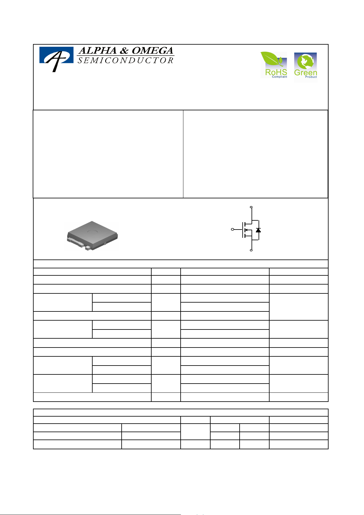
Ultra SO-8
S
G
Drain-Source Voltage
Gate-Source Voltage
Continuous Drain
Current
B
Pulsed Drain Current
Continuous Drain
Current
H
Avalanche Current
Repetitive avalanche energy L=0.3mH
Power Dissipation
Power Dissipation
Junction and Storage Temperature Range
DS(ON)
C
B
A
, low gate charge.This device
TM
Top View
D
Bottom tab
connected to
A
V
DS
V
GS
=25°C
T
C
T
=100°C
C
I
D
I
DM
TA=25°C
T
=70°C
A
TC=25°C
TC=100°C
TA=25°C
=70°C
T
A
I
DSM
I
C
AR
E
AR
P
D
P
DSM
TJ, T
STG
Features
(V) = 30V
DS
= 46A (VGS = 10V)
I
D
R
R
UIS Tested
Rg,Ciss,Coss,Crss Tested
< 10.5mΩ (VGS = 10V)
DS(ON)
< 13.5mΩ (VGS = 4.5V)
DS(ON)
G
Maximum UnitsParameter
30
46
33
120
10
8
30
135 mJ
43
21
2
1.2
-55 to 175
D
S
V
V±12
A
A
A
W
W
°C
Thermal Characteristics
Parameter Units
Maximum Junction-to-Ambient
Maximum Junction-to-Ambient
Maximum Junction-to-Case
Alpha & Omega Semiconductor, Ltd.
t ≤ 10s
Steady-State
C
Steady-State
R
θJA
R
θJC
24 30
53 64
2.4 3.5
°C/W
°C/W
°C/W
www.aosmd.com
AOL1426
Electrical Characteristics (T
Symbol Min Typ Max Units
=25°C unless otherwise noted)
J
Parameter Conditions
STATIC PARAMETERS
BV
I
DSS
I
GSS
V
GS(th)
I
D(ON)
R
DS(ON)
g
FS
V
SD
I
S
DSS
Drain-Source Breakdown Voltage
Zero Gate Voltage Drain Current
Gate-Body leakage current
Gate Threshold Voltage
On state drain current
Static Drain-Source On-Resistance
Forward Transconductance
Diode Forward Voltage
Maximum Body-Diode Continuous Current
I
D
V
=30V, VGS=0V
DS
V
=0V, VGS= ±12V
DS
V
DS=VGS ID
=250µA
VGS=10V, VDS=5V
V
=10V, ID=20A
GS
V
=4.5V, ID=20A
GS
=5V, ID=20A
V
DS
=1A,VGS=0V
I
S
=55°C 5
T
J
=125°C 14.5 18
T
J
30 V
1
uA
0.1 µA
1 1.55 2.5 V
120 A
8.5 10.5
mΩ
10.2 13.5 mΩ
40 S
0.73 1.0 V
46 A
=250µA, VGS=0V
DYNAMIC PARAMETERS
C
iss
C
oss
C
rss
R
g
Input Capacitance
Output Capacitance
Reverse Transfer Capacitance
Gate resistance
=0V, VDS=15V, f=1MHz
V
GS
=0V, VDS=0V, f=1MHz
V
GS
1210 1452 pF
330 pF
85 pF
1.2 1.6 Ω
SWITCHING PARAMETERS
(10V) 22 28 nC
Q
g
Q
(4.5V) 10 13 nC
g
Q
gs
Q
gd
t
D(on)
t
r
t
D(off)
t
f
t
rr
Q
rr
A: The value of R
B. The power dissipation P
dissipation limit for cases where additional heatsinking is used.
C: Repetitive rating, pulse width limited by junction temperature T
D. The R
E. The static characteristics in Figures 1 to 6 are obtained using <300 µs pulses, duty cycle 0.5% max.
F. These curves are based on the junction-to-case thermal impedence which is measured with the device mounted to a large heatsink,
assuming a maximum junction temperature of T
G. These tests are performed with the device mounted on 1 in
curve provides a single pulse rating.
H. Surface mounted on a 1 in 2 FR-4 board with 2oz. Copper.
* This device is guaranteed green after date code 8P11 (June 1
Rev5: Dec 2008
THIS PRODUCT HAS BEEN DESIGNED AND QUALIFIED FOR THE CONSUMER MARKET. APPLICATIONS OR USES AS CRITICAL
COMPONENTS IN LIFE SUPPORT DEVICES OR SYSTEMS ARE NOT AUTHORIZED. AOS DOES NOT ASSUME ANY LIABILITY ARISING
OUT OF SUCH APPLICATIONS OR USES OF ITS PRODUCTS. AOS RESERVES THE RIGHT TO IMPROVE PRODUCT DESIGN,
FUNCTIONS AND RELIABILITY WITHOUT NOTICE.
Total Gate Charge
Total Gate Charge
Gate Source Charge
VGS=10V, VDS=15V, ID=20A
Gate Drain Charge
Turn-On DelayTime
Turn-On Rise Time
Turn-Off DelayTime
V
R
Turn-Off Fall Time
I
Body Diode Reverse Recovery Time
Body Diode Reverse Recovery Charge
is measured with the device in a still air environment with T A =25°C.
θJA
is the sum of the thermal impedence from junction to case R
θJA
is based on T
D
=175°C, using junction-to-case thermal resistance, and is more useful in setting the upper
J(MAX)
=175°C.
J(MAX)
F
I
F
2
FR-4 board with 2oz. Copper, in a still air environment with T A=25°C. The SOA
ST
=10V, VDS=15V, RL=0.75Ω,
GS
=3Ω
GEN
=20A, dI/dt=100A/µs
=20A, dI/dt=100A/µs
=175°C.
J(MAX)
2008)
and case to ambient.
θJC
3.7 nC
2.7 nC
10 ns
6.3 ns
21 ns
2.8 ns
36
45 ns
47 nC
Alpha & Omega Semiconductor, Ltd. www.aosmd.com
 Loading...