

Alpha & Omega Semiconductor AOL1420 Service Manual
查询AOL1401供应商
AOL1420
N-Channel Enhancement Mode Field Effect Transistor
General Description
The AOL1420 uses advanced trench technology to
provide excellent R
gate resistance. This device is ideally suited for use
as a low side switch in CPU core power conversion.
Standard Product AOL1420 is Pb-free (meets ROHS
& Sony 259 specifications). AOL1420L is a Green
Product ordering option. AOL1420 and AOL1420L
are electrically identical.
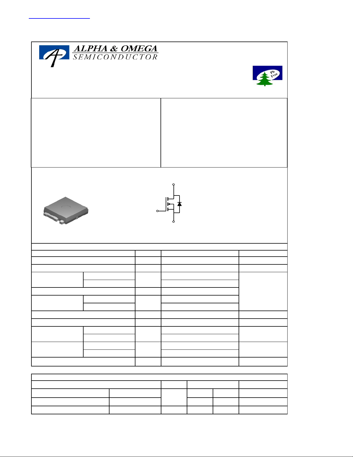
UltraSO-8
TM
S
G
Absolute Maximum Ratings T
Drain-Source Voltage
Gate-Source Voltage
Continuous Drain
Current
B,G
Pulsed Drain Current
Continuous Drain
Current
G
Avalanche Current
Repetitive avalanche energy L=0.1mH
Power Dissipation
Power Dissipation
Junction and Storage Temperature Range
, low gate charge and low
DS(ON)
Top View
Fits SOIC8
footprint !
D
Bottom tab
connected to
drain
=25°C unless otherwise noted
A
Symbol
V
DS
V
GS
I
D
I
DM
=25°C
T
C
TC=100°C
G
B
TA=25°C
T
=70°C 14
A
C
TC=25°C
B
T
=100°C
C
TA=25°C
A
T
=70°C 1.3
A
I
DSM
I
C
AR
E
AR
P
D
P
DSM
TJ, T
STG
Features
VDS (V) = 30V
= 85A (VGS = 10V)
I
D
R
DS(ON)
R
DS(ON)
D
G
S
< 3.7mΩ (VGS = 10V)
< 5.5mΩ (VGS = 4.5V)
Maximum UnitsParameter
30
85
63
150
18
30
112 mJ
100
50
2.1
-55 to 175
V
V±20
A
A
W
W
°C
Thermal Characteristics
Parameter Units
Maximum Junction-to-Ambient
Maximum Junction-to-Ambient
Maximum Junction-to-Case
C
A
A
t ≤ 10s
Steady-State
Steady-State
Symbol Typ Max
R
θJA
19.6 25
50 60
R
θJC
0.9 1.5
°C/W
°C/W
°C/W
Alpha & Omega Semiconductor, Ltd.
AOL1420
j
Electrical Characteristics (T
Symbol Min Typ Max Units
=25°C unless otherwise noted)
J
Parameter Conditions
STATIC PARAMETERS
BV
I
DSS
I
GSS
V
GS(th)
I
D(ON)
R
DS(ON)
g
FS
V
SD
I
S
DSS
Drain-Source Breakdown Voltage
Zero Gate Voltage Drain Current
Gate-Body leakage current
Gate Threshold Voltage V
On state drain current
Static Drain-Source On-Resistance
Forward Transconductance
Diode Forward Voltage
Maximum Body-Diode Continuous Current
I
=250μA, VGS=0V
D
V
=24V, VGS=0V
DS
=0V, VGS= ±20V
V
DS
DS=VGS ID
V
GS
V
GS
=250μA
=10V, VDS=5V
=10V, ID=20A
VGS=4.5V, ID=20A
=5V, ID=20A
V
DS
I
=1A,VGS=0V
S
30 V
T
=55°C 5
J
1 1.8 3 V
85 A
2.9 3.7
T
=125°C 4.4 5.5
J
4.4 5.5
106 S
0.72 1 V
1
μA
100 nA
mΩ
mΩ
85 A
DYNAMIC PARAMETERS
C
iss
C
oss
C
rss
R
g
Input Capacitance
Output Capacitance
Reverse Transfer Capacitance
Gate resistance V
=0V, VDS=15V, f=1MHz
V
GS
=0V, VDS=0V, f=1MHz
GS
3200 3840 pF
590 pF
414 pF
0.54 0.7 Ω
SWITCHING PARAMETERS
Q
(10V) 63 76 nC
g
Q
(4.5V) 33 40 nC
g
Q
gs
Q
gd
t
D(on)
t
r
t
D(off)
t
f
t
rr
Q
rr
A: The value of R qJA is measured with the device in a still air environment with T A =25°C.
B. The power dissipation PD is based on TJ(MAX)=175°C, using junction-to-case thermal resistance, and is more useful in setting the upper
dissipation limit for cases where additional heatsinking is used.
C: Repetitive rating, pulse width limited by junction temperature TJ(MAX)=175°C.
D. The R qJA is the sum of the thermal impedence from junction to case R qJC and case to ambient.
E. The static characteristics in Figures 1 to 6 are obtained using <300 ms pulses, duty cycle 0.5% max.
F. These curves are based on the
a maximum junction temperature of TJ(MAX)=175°C.
G. The maximum current rating is limited by bond-wires.
Rev0: August 2005
Total Gate Charge
Total Gate Charge
Gate Source Charge
Gate Drain Charge
Turn-On DelayTime
Turn-On Rise Time
Turn-Off DelayTime
Turn-Off Fall Time
Body Diode Reverse Recovery Time
Body Diode Reverse Recovery Charge
unction-to-case thermal impedence which is measured with the device mounted to a large heatsink, assuming
=4.5V, VDS=15V, ID=20A
V
GS
V
=10V, VDS=15V, RL=0.75Ω,
GS
R
=3Ω
GEN
=20A, dI/dt=100A/μs
I
F
I
=20A, dI/dt=100A/μs
F
8.6 nC
17.6 nC
12 ns
15.5 ns
40 ns
14 ns
34
41 ns
30 nC
THIS PRODUCT HAS BEEN DESIGNED AND QUALIFIED FOR THE CONSUMER MARKET. APPLICATIONS OR USES AS CRITICAL
COMPONENTS IN LIFE SUPPORT DEVICES OR SYSTEMS ARE NOT AUTHORIZED. AOS DOES NOT ASSUME ANY LIABILITY ARISING
OUT OF SUCH APPLICATIONS OR USES OF ITS PRODUCTS. AOS RESERVES THE RIGHT TO IMPROVE PRODUCT DESIGN,
FUNCTIONS AND RELIABILITY WITHOUT NOTICE.
Alpha & Omega Semiconductor, Ltd.
 Loading...