

Alpha & Omega Semiconductor AO4704 Service Manual
A
查询AO4600供应商
AO4704
N-Channel Enhancement Mode Field Effect Transistor with
Schottky Diode
General Description
The AO4704 uses advanced trench technology to
provide excellent R
body diode characteristics. This device is suitable for
use as a synchronous switch in PWM applications.
The co-packaged Schottky Diode boosts efficiency
further. AO4704 is Pb-free (meets ROHS & Sony
259 specifications). AO4704L is a Green Product
ordering option. AO4704 and AO4704L are
shoot-through immunity and
DS(ON),
Features
VDS (V) = 30V
= 13 A (VGS = 10V)
I
D
< 11.5mΩ (VGS = 10V)
R
DS(ON)
R
< 13mΩ (VGS = 4.5V)
DS(ON)
SCHOTTKY
VDS (V) = 30V, IF = 3A, VF<0.5V@1A
electrically identical.
D
K
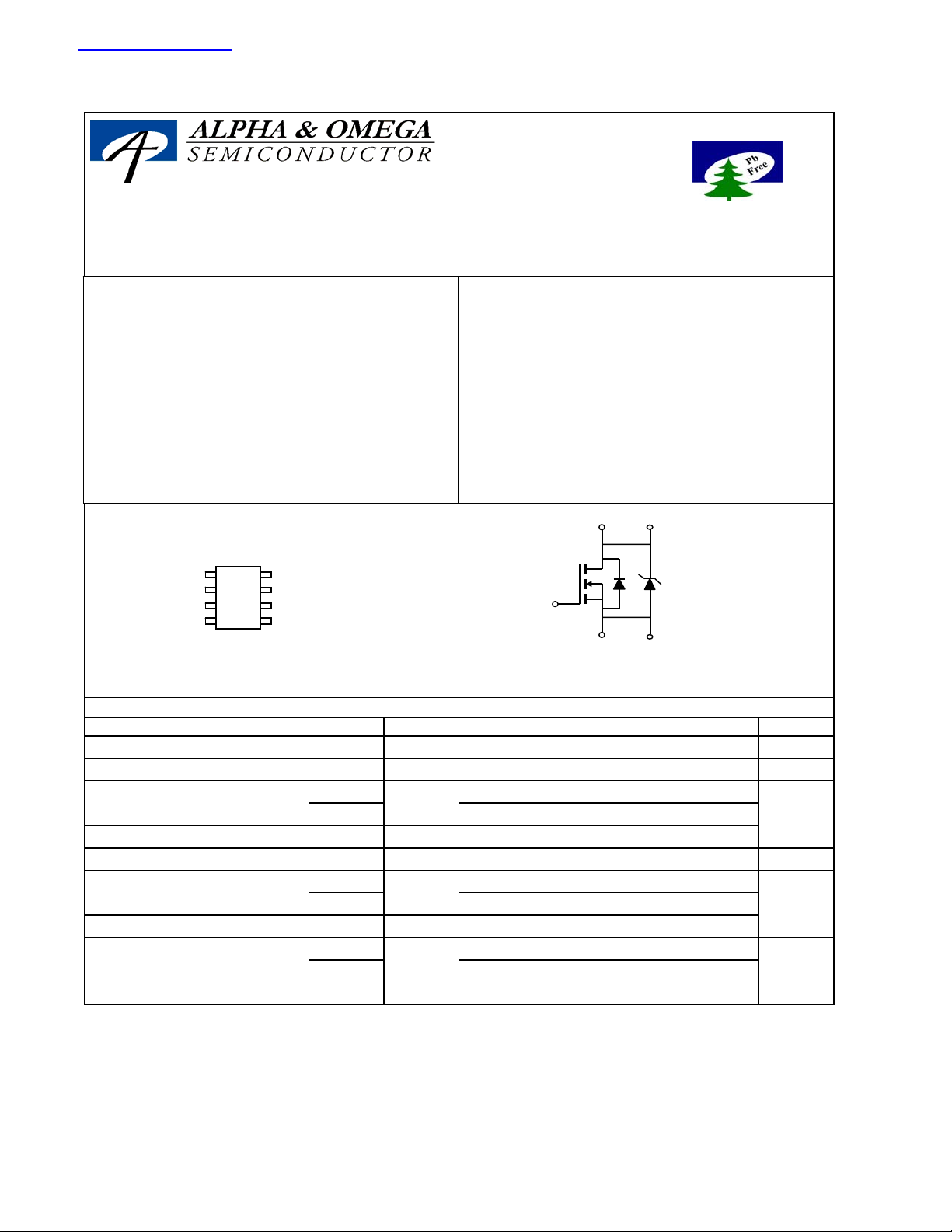
SOIC-8
1
8
S/A
2
S/A
3
S/A
4
G
Absolute Maximum Ratings TA=25°C unless otherwise noted
Parameter MOSFET Schottky
Drain-Source Voltage 30
Gate-Source Voltage
Continuous Drain Current
Pulsed Drain Current
B
Schottky reverse voltage 30
Continuous Forward Current
Pulsed Diode Forward Current
Power Dissipation
D/K
7
D/K
6
D/K
5
D/K
G
S
Symbol Units
V
DS V
V
GS V
T
=25°C
A
A
=70°C
T
A
=25°C
T
A
A
=70°C
T
A
B
TA=25°C
=70°C
T
A
I
D
I
DM
V
KA V
I
F
I
FM
P
D
, T
T
J
STG °CJunction and Storage Temperature Range -55 to 150 -55 to 150
±12
13
10.4
40
4.4
3.2
30
3.1 3.1
22
A
A
W
Alpha & Omega Semiconductor, Ltd.
AO4704
Thermal Characteristics
Parameter Units
Maximum Junction-to-Ambient
Maximum Junction-to-Lead
A
A
C
t ≤ 10s
Steady-State
Steady-State
Symbol Typ Max
R
θJA
R
θJL
28 40
54 75
21 30
°C/W
°C/WMaximum Junction-to-Ambient
°C/W
Thermal Characteristics: Schottky
Parameter Units
Maximum Junction-to-Ambient
Maximum Junction-to-Ambient
Maximum Junction-to-Lead
A: The value of R
value in any given application depends on the user's specific board design. The current rating is based on the t ≤ 10s thermal resistance rating.
B: Repetitive rating, pulse width limited by junction temperature.
C. The R
θJA
D. The static characteristics in Figures 1 to 6 are obtained using 80 µs pulses, duty cycle 0.5% max.
E. These tests are performed with the device mounted on 1 in
curve provides a single pulse rating.
F. The Schottky appears in parallel with the MOSFET body diode, even though it is a separate chip. Therefore, we provide the net forward drop,
capacitance and recovery characteristics of the MOSFET and Schottky. However, the thermal resistance is specified for each chip
separately.
Rev5: August 2005
THIS PRODUCT HAS BEEN DESIGNED AND QUALIFIED FOR THE CONSUMER MARKET. APPLICATIONS OR USES AS CRITICAL COMPONENTS
IN LIFE SUPPORT DEVICES OR SYSTEMS ARE NOT AUTHORIZED. AOS DOES NOT ASSUME ANY LIABILITY ARISINGOUT OF SUCH APPLICATIONS
OR USES OF ITS PRODUCTS. AOS RESERVES THE RIGHT TO IMPROVE PRODUCT DESIGN,FUNCTIONS AND RELIABILITY WITHOUT NOTICE.
is measured with the device mounted on 1in 2 FR-4 board with 2oz. Copper, in a still air environment with T A=25°C. The
θJA
is the sum of the thermal impedence from junction to lead R
A
A
C
t ≤ 10s
Steady-State
Steady-State
Symbol Typ Max
R
θJA
R
θJL
and lead to ambient.
θJL
2
FR-4 board with 2oz. Copper, in a still air environment with T A=25°C. The SOA
36 40
67 75
25 30
°C/W
°C/W
°C/W
 Loading...