

Alpha & Omega Semiconductor AO4609 Service Manual
A
A
A
A
p
查询AO4609供应商
AO4609
Complementary Enhancement Mode Field Effect Transistor
July 2003
General Description
Features
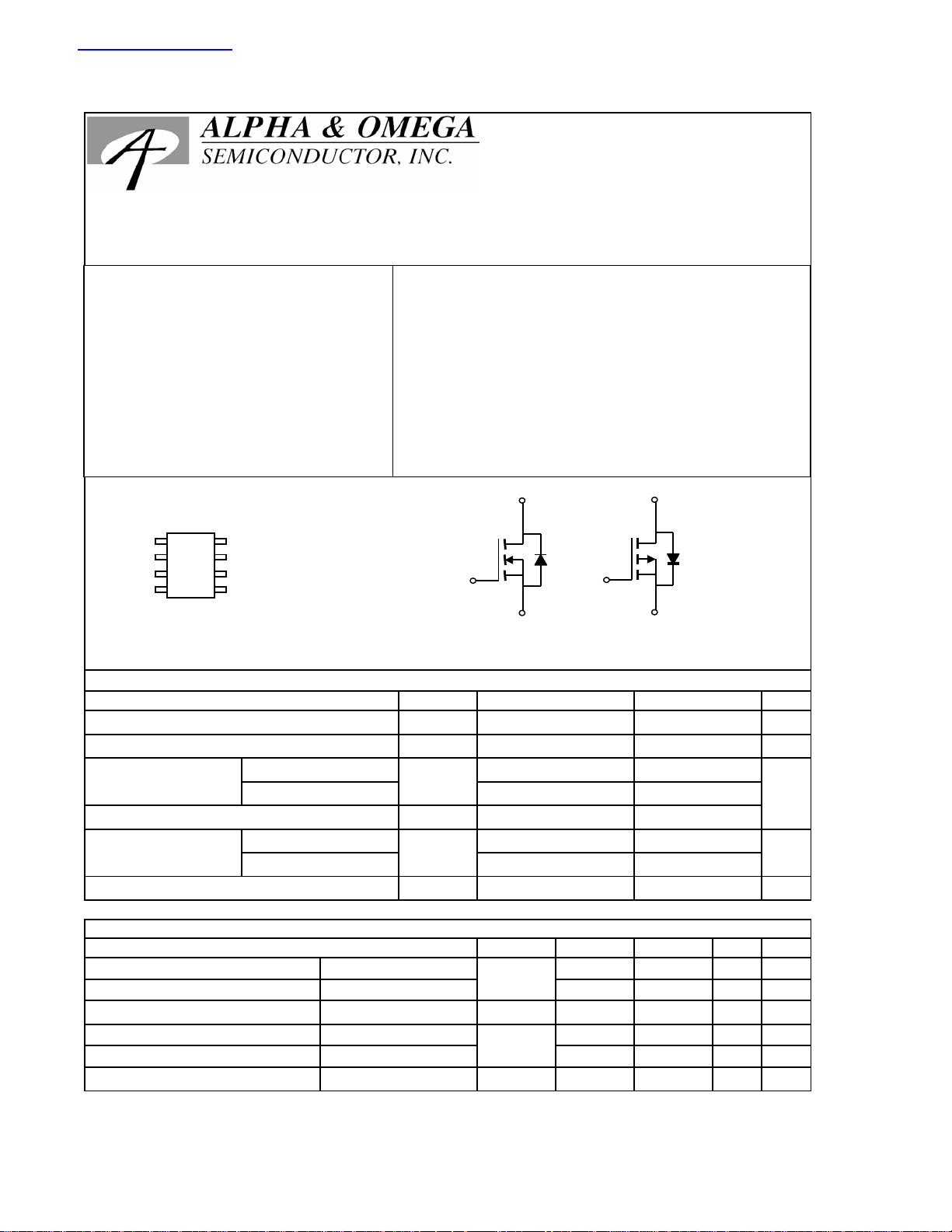
n-channel p-channel
The AO4609 uses advanced trench
technology MOSFETs to provide
excellent R
and low gate charge.
DS(ON)
The complementary MOSFETs may be
used to form a level shifted high side
switch, and for a host of other
applications.
1
8
S2
G2
S1
G1
2
3
4
D2
7
D2
6
D1
5
D1
SOIC-8
Absolute Maximum Ratings T
=25°C unless otherwise noted
A
Parameter Max n-channel
Drain-Source Voltage 30
Gate-Source Voltage ±20 ±12
Continuous Drain
Current
A
Pulsed Drain Current
Power Dissipation
TA=25°C
T
=70°C 6.6 -2.4
A
B
=25°C
T
A
T
=70°C 1.28 1.28
A
Junction and Storage Temperature Range -55 to 150 -55 to 150
(V) = 30V -30V
V
DS
I
= 8.5A -3A
D
R
DS(ON) RDS(ON)
< 18mΩ (VGS=10V) < 130mΩ (VGS = 10V)
< 28mΩ (V
< 260mΩ (V
=4.5V) < 180mΩ (VGS = 4.5V)
GS
D2
G2
S2
n-channel
G1
-channel
GS
D1
S1
= 2.5V)
Symbol Max p-channel Units
V
DS
V
GS
I
D
I
DM
P
D
TJ, T
8.5
40 -6
22
STG
-30
-3
V
V
A
W
°C
Thermal Characteristics: n-channel and p-channel
Parameter
Maximum Junction-to-Ambient
Maximum Junction-to-Ambient
Maximum Junction-to-Lead
C
Maximum Junction-to-Ambient
Maximum Junction-to-Ambient
Maximum Junction-to-Lead
C
t ≤ 10s
Steady-State
Steady-State
t ≤ 10s
Steady-State
Steady-State
Symbol Device Typ Max Units
R
θJA
R
θJL
R
θJA
R
θJL
n-ch 48 62.5 °C/W
n-ch 74 110 °C/W
n-ch 35 40 °C/W
p-ch 56 62.5 °C/W
p-ch 81 110 °C/W
p-ch 40 48 °C/W
AO4609
Ω
N-Channel Electrical Characteristics (TJ=25°C unless otherwise noted)
Symbol Min Typ Max Units
Parameter Conditions
STATIC PARAMETERS
BV
DSS
I
DSS
I
GSS
V
GS(th)
I
D(ON)
R
DS(ON)
g
FS
V
SD
I
S
Drain-Source Breakdown Voltage
Zero Gate Voltage Drain Current
Gate-Body leakage current
I
=250µA, VGS=0V
D
VDS=24V, VGS=0V
VDS=0V, VGS= ±20V
Gate Threshold Voltage VDS=V
On state drain current
VGS=10V, VDS=5V
VGS=10V, ID=8.5A
Static Drain-Source On-Resistance
VGS=4.5V, ID=6A
Forward Transconductance
Diode Forward Voltage
VDS=5V, ID=8.5A
IS=1A,VGS=0V
Maximum Body-Diode Continuous Current
GS ID
=250µA
TJ=55°C
TJ=125°C
30 V
1
5
µA
100 nA
1 1.8 3 V
30 A
15.5 18
22.3 27
23 28
mΩ
m
23 S
0.75 1 V
3A
DYNAMIC PARAMETERS
C
iss
C
oss
C
rss
R
g
Input Capacitance
Output Capacitance
VGS=0V, VDS=15V, f=1MHz
Reverse Transfer Capacitance
Gate resistance VGS=0V, VDS=0V, f=1MHz
1040 pF
180 pF
110 pF
0.7 Ω
SWITCHING PARAMETERS
Qg(10V)
Qg(4.5V)
Q
gs
Q
gd
t
D(on)
t
r
t
D(off)
t
f
t
rr
Q
rr
Total Gate Charge
Total Gate Charge
Gate Source Charge
Gate Drain Charge
Turn-On DelayTime
Turn-On Rise Time
Turn-Off DelayTime
Turn-Off Fall Time
Body Diode Reverse Recovery Time
Body Diode Reverse Recovery Charge
VGS=10V, VDS=15V, ID=8.5A
VGS=10V, VDS=15V, RL=1.8Ω,
R
=3Ω
GEN
IF=8.5A, dI/dt=100A/µs
IF=8.5A, dI/dt=100A/µs
19.2 nC
9.36 nC
2.6 nC
4.2 nC
5.2 ns
4.4 ns
17.3 ns
3.3 ns
16.7
ns
6.7 nC
A: The value of R
in any a given application depends on the user's specific board design. The current rating is based on the t ≤ 10s thermal resistance rating.
B: Repetitive rating, pulse width limited by junction temperature.
C. The R
D. The static characteristics in Figures 1 to 6 are obtained using 80 µs pulses, duty cycle 0.5% max.
E. These tests are performed with the device mounted on 1 in
curve provides a single pulse rating.
θJA
is measured with the device mounted on 1in 2 FR-4 board with 2oz. Copper, in a still air environment with T A=25°C. The value
θJA
is the sum of the thermal impedence from junction to lead R
2
FR-4 board with 2oz. Copper, in a still air environment with T A=25°C. The SOA
and lead to ambient.
θJL
Alpha & Omega Semiconductor, Ltd.
AO4609
Ω
Ω
P-Channel Electrical Characteristics (TJ=25°C unless otherwise noted)
Symbol Min Typ Max Units
Parameter Conditions
STATIC PARAMETERS
BV
I
DSS
I
GSS
V
GS(th)
I
D(ON)
R
DS(ON)
g
FS
V
SD
I
S
DSS
Drain-Source Breakdown Voltage
Zero Gate Voltage Drain Current
Gate-Body leakage current
I
=-250µA, VGS=0V
D
VDS=-24V, VGS=0V
VDS=0V, VGS=±12V
Gate Threshold Voltage VDS=V
On state drain current
VGS=-4.5V, VDS=-5V
VGS=-10V, ID=-3A
Static Drain-Source On-Resistance
VGS=-4.5V, ID=-2A
VGS=-2.5V, ID=-1A
Forward Transconductance
Diode Forward Voltage
VDS=-5V, ID=-3A
IS=-1A,VGS=0V
Maximum Body-Diode Continuous Current
GS ID
=-250µA
TJ=55°C
TJ=125°C
-30 V
-1
-5
µA
±100 nA
-0.6 -1 -1.4 V
-10 A
102 130
154 200
128 180
187 260
mΩ
m
m
3 4.5 S
-0.85 -1 V
-2 A
DYNAMIC PARAMETERS
C
iss
C
oss
C
rss
R
g
Input Capacitance
Output Capacitance
VGS=0V, VDS=-15V, f=1MHz
Reverse Transfer Capacitance
Gate resistance VGS=0V, VDS=0V, f=1MHz
409 pF
55 pF
42 pF
12 Ω
SWITCHING PARAMETERS
Q
Q
Q
t
D(on)
t
r
t
D(off)
t
f
t
rr
Q
g
gs
gd
Total Gate Charge
Gate Source Charge
Gate Drain Charge
VGS=-4.5V, VDS=-15V, ID=-3A
Turn-On DelayTime
Turn-On Rise Time
Turn-Off DelayTime
VGS=-10V, VDS=-15V, RL=5Ω,
R
=3Ω
GEN
Turn-Off Fall Time
Body Diode Reverse Recovery Time
rr
Body Diode Reverse Recovery Charge
IF=-3A, dI/dt=100A/µs
IF=-3A, dI/dt=100A/µs
4.4 nC
0.8 nC
1.32 nC
5.3 ns
4.4 ns
31.5 ns
8ns
15.8
ns
8nC
A: The value of R
value in any a given application depends on the user's specific board design. The current rating is based on the t ≤ 10s thermal resistance
rating.
B: Repetitive rating, pulse width limited by junction temperature.
C. The R
D. The static characteristics in Figures 1 to 6,12,14 are obtained using 80 µs pulses, duty cycle 0.5% max.
E. These tests are performed with the device mounted on 1 in
SOA curve provides a single pulse rating.
θJA
is measured with the device mounted on 1in 2 FR-4 board with 2oz. Copper, in a still air environment with T
θJA
is the sum of the thermal impedence from junction to lead R
2
FR-4 board with 2oz. Copper, in a still air environment with T A=25°C. The
and lead to ambient.
θJL
=25°C. The
A
Alpha & Omega Semiconductor, Ltd.
AO4609
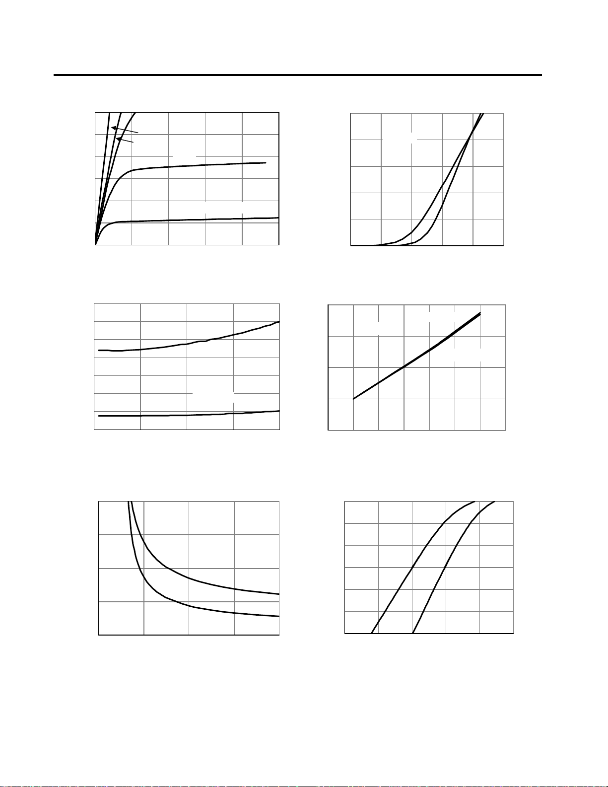
N-CHANNEL: TYPICAL ELECTRICAL AND THERMAL CHARACTERISTICS
30
25
4V
10V
4.5V
20
15
(A)
D
I
10
3.5V
VGS=3V
5
0
012345
V
(Volts)
DS
Fig 1: On-Region Characteristics
28
)
Ω
(m
DS(ON)
R
26
24
22
20
18
V
=4.5V
GS
VGS=10V
16
14
0 5 10 15 20
I
(A)
D
Figure 3: On-Resistance vs. Drain Current and
Gate Voltage
2.00E+01
1.60E+01
VDS=5V
1.20E+01
(A)
D
I
8.00E+00
125°C
25°C
4.00E+00
0.00E+00
1.5 2 2.5 3 3.5 4
V
(Volts)
GS
Figure 2: Transfer Characteristics
1.6
VGS=10V
ID=8.5A
1.4
VGS=4.5V
1.2
1
Normalized On-Resistance
0.8
0 25 50 75 100 125 150 175
Temperature (°C)
Figure 4: On-Resistance vs. Junction
Temperature
50
)
Ω
(m
DS(ON)
R
40
30
20
25°C
ID=8.5A
10
246810
V
(Volts)
GS
Figure 5: On-Resistance vs. Gate-Source Voltage
Alpha & Omega Semiconductor, Ltd.
125°C
1.0E+01
1.0E+00
1.0E-01
(A)
1.0E-02
S
I
1.0E-03
1.0E-04
1.0E-05
125°C
25°C
0.0 0.2 0.4 0.6 0.8 1.0
V
(Volts)
SD
Figure 6: Body-Diode Characteristics
 Loading...