

ALPHA & OMEGA SEMICONDUCTOR AO4423 Datasheet
AO4423/AO4423L
Symbol
Symbol
Typ
Max
A
AF
Absolute Maximum Ratings T
=25°C unless otherwise noted
B
D
D
D
D
S
S
S
G
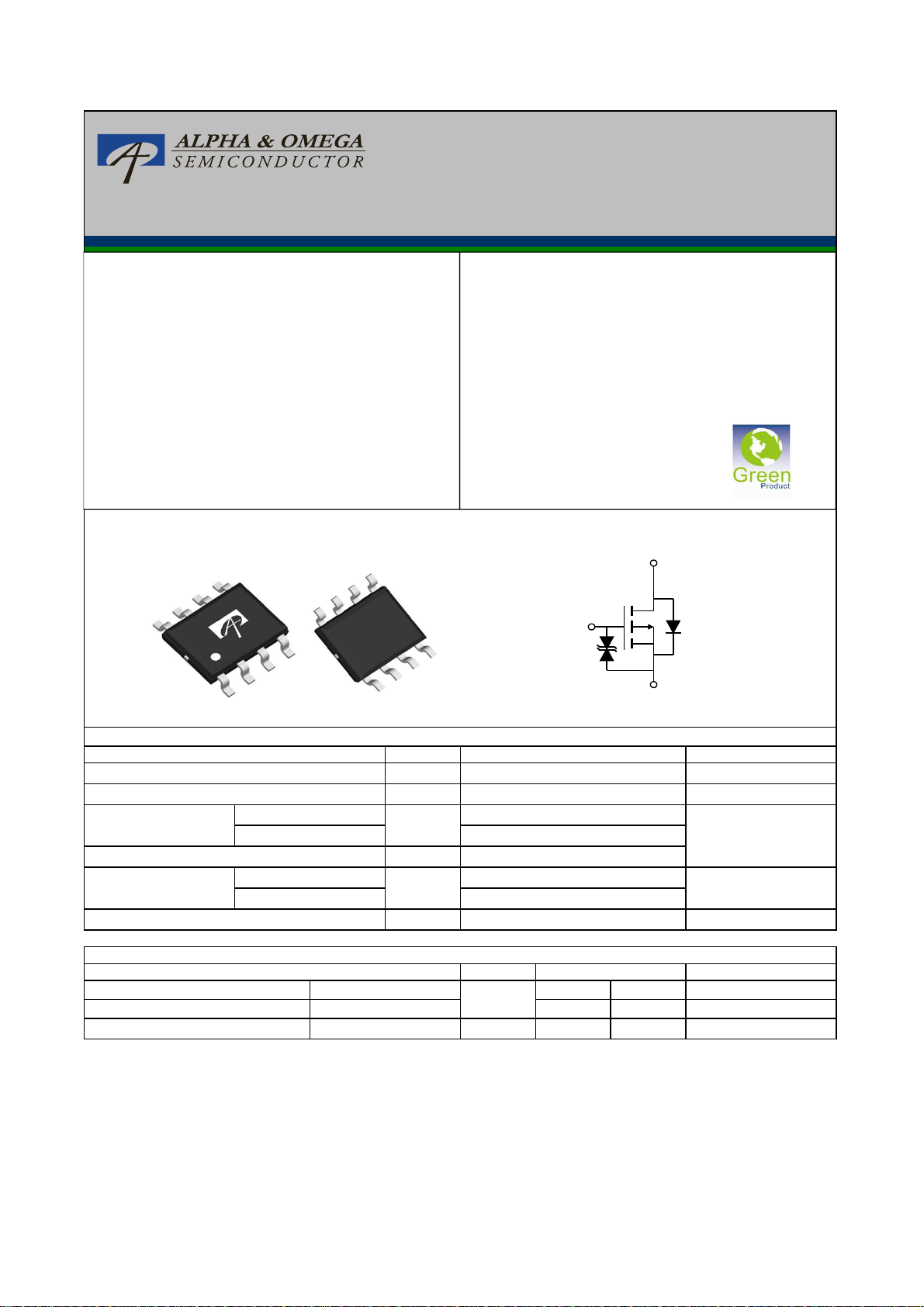
30V P-Channel MOSFET
General Description
The AO4423/AO4423L uses advanced trench technology
to provide excellent R
with a 25V gate rating. This device is suitable for use as a
load switch or in PWM applications.
* RoHS and Halogen-Free Compliant
Top View Bottom View
, and ultra-low low gate charge
DS(ON)
SOIC-8
Product Summary
VDS(V) = -30V
ID= -17A (VGS= -20V)
R
< 6.2mΩ (V
DS(ON)
R
< 7.2mΩ (V
DS(ON)
ESD Protected
100% UIS tested
100% Rg tested (note *)
G
GS
GS
= -20V)
= -10V)
D
S
A
Maximum UnitsParameter
Drain-Source Voltage -30
Continuous Drain
Current
AF
TA=25°C
TA=70°C I
TA=25°C
A
Power Dissipation
TA=70°C
Junction and Storage Temperature Range °C
V
DS
V
GS
D
I
DM
P
D
TJ, T
STG
±25Gate-Source Voltage
-17
-14
-182Pulsed Drain Current
3.1
2
-55 to 150
W
Thermal Characteristics
Parameter
Maximum Junction-to-Ambient
Maximum Junction-to-Ambient
Maximum Junction-to-Lead
C
t ≤ 10s
Steady-State
Steady-State
R
θJA
R
θJL
26 40
50 75
14 24
Units
°C/W
°C/W
°C/W
V
V
A
Rev.12.0 August 2017
www.aosmd,com
APPLICATIONS OR USE AS CRITICAL COMPONENTS IN LIFE SUPPORT DEVICES OR SYSTEMS ARE NOT AUTHORIZED. AOS DOES NOT
ASSUME ANY LIABILITY ARISING OUT OF SUCH APPLICATIONS OR USES OF ITS PRODUCTS. AOS RESERVES THE RIGHT TO IMPROVE
Electrical Characteristics (TJ=25°C unless otherwise noted)
Symbol Min Typ Max Units
Parameter Conditions
STATIC PARAMETERS
BV
I
DSS
I
GSS
V
GS(th)
I
D(ON)
R
DS(ON)
g
FS
V
SD
I
S
DSS
Drain-Source Breakdown Voltage
Zero Gate Voltage Drain Current
Gate-Body leakage current
Gate Threshold Voltage
On state drain current
Static Drain-Source On-Resistance
Forward Transconductance
Diode Forward Voltage
Maximum Body-Diode Continuous Current
=-250µA, V
D
VDS=-30V, VGS=0V
VDS=0V, VGS=±20V
VDS=0V, VGS=±25V
VDS=V
GS ID
VGS=-10V, VDS=-5V
VGS=-20V, ID=-15A
VGS=-10V, ID=-15A
VGS=-6V, ID=-10A
VDS=-5V, ID=-15A
IS=-1A,VGS=0V
=0V
GS
=-250µA
-30 V
TJ=55°C -5
±10 µA
-1.5 -2.1 -2.6 V
-182 A
5.1 6.2
TJ=125°C 7.4 9
5.9 7.2 mΩ
7.5 9.5 mΩ
48 S
-0.71 -1 V
-4.2 A
-1
µA
±1 µA
mΩ
I
DYNAMIC PARAMETERS
C
iss
C
oss
C
rss
R
g
Input Capacitance
Output Capacitance
Reverse Transfer Capacitance
Gate resistance
VGS=0V, VDS=-15V, f=1MHz
VGS=0V, VDS=0V, f=1MHz
2.1 4.3 6.4 Ω
2527 3033 pF
583 pF
397 556 pF
SWITCHING PARAMETERS
Q
g
Q
gs
Q
gd
t
D(on)
t
r
t
D(off)
t
f
t
rr
Q
rr
A: The value of R
T A=25°C. The value in any given application depends on the user's specific board design.
B: Repetitive rating, pulse width limited by junction temperature.
C. The R
D. The static characteristics in Figures 1 to 6 are obtained using <300 µs pulses, duty cycle 0.5% max.
E. These tests are performed with the device mounted on 1 in 2 FR-4 board with 2oz. Copper, in a still air environment with T A=25°C. The SOA
curve provides a single pulse rating.
F. The current rating is based on the t≤ 10s junction to ambient thermal resistance rating.
Note *: This device is guaranteed RG 100% tested after date code 8V11 (Jan 1st 2008)
Total Gate Charge
Gate Source Charge
Gate Drain Charge
Turn-On DelayTime
Turn-On Rise Time
Turn-Off DelayTime
Turn-Off Fall Time
Body Diode Reverse Recovery Time
Body Diode Reverse Recovery Charge
is measured with the device mounted on 1in 2 FR-4 board with 2oz. Copper, in a still air environment with
θJA
is the sum of the thermal impedence from junction to lead R
θJA
VGS=-10V, VDS=-15V, ID=-15A
VGS=-10V, VDS=-15V, R
R
=3Ω
GEN
I
=-15A, dI/dt=100A/µs
F
I
=-15A, dI/dt=100A/µs
F
and lead to ambient.
θJL
=1.0Ω,
L
47 57 nC
8 nC
14 nC
12 ns
8 ns
54 ns
87 ns
26.1 32
ns
12.3 nC
PRODUCT DESIGN,FUNCTIONS AND RELIABILITY WITHOUT NOTICE.
Rev.12.0 August 2017
www.aosmd,com
 Loading...