

Alpha & Omega AOZ1237QI-02 Schematic [ru]

AOZ1237QI-02
24V/8A Synchronous EZBuckTM Regulator
General Description
The AOZ1237 is a high-efficiency, easy-to-use DC/DC
synchronous buck regulator that operates up to 24V.
The device is capable of supplying 8A of continuous
output current with an output voltage adjustable down to
0.8V (±1.0%).
A proprietary constant on-time PWM control with input
feed-forward results in ultra-fast transient response while
maintaining relatively constant switching frequency over
the entire input voltage range. The switching frequency
can be externally programmed up to 1MHz.
The device features multiple protection functions such as
V
under-voltage lockout, cycle-by-cycle current limit,
CC
output over-voltage protection, short-circuit protection, as
well as thermal shutdown.
The AOZ1237 is available in a 4mm x 4mm QFN-23L
package and is rated over a -40°C to +85°C ambient
temperature range.
Features
Wide input voltage range
– 2.7V to 24V
8A continuous output current
Output voltage adjustable down to 0.8V (±1.0%)
Low R
– 35m high-side
– 8m low-side SRFET™
Constant On-Time with input feed-forward
Programmable frequency up to 1MHz
Selectable PFM light load operation
Ceramic capacitor stable
Adjustable soft start
Power Good output
Integrated bootstrap diode
Cycle-by-cycle current limit
Short-circuit protection
Over voltage protection
Thermal shutdown
Thermally enhanced 4mm x 4mm QFN-23L package
internal NFETs
DS(ON)
Applications
Portable computers
Compact desktop PCs
Servers
Graphics cards
Set-top boxes
LCD TVs
Cable modems
Point-of-load DC/DC converters
Telecom/Networking/Datacom equipment
Rev. 2.0 April 2013
www.aosmd.com
Page 1 of 15

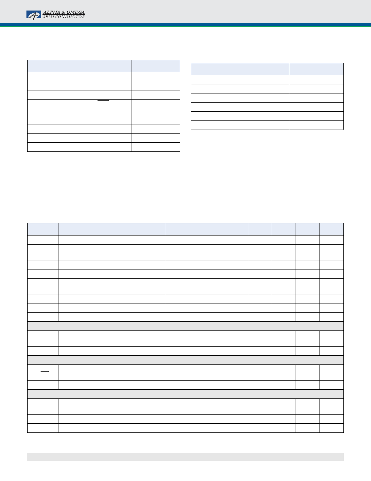
Typical Application
5V
Power Good
Off On
R3
100kΩ
R
TON
C4
1μF
C
SS
TON IN
VCC
AOZ1237
PGOOD
EN
PFM
SS
Power Ground
Analog Ground
BST
LX
FB
AGND
PGND
C5
0.1μF
L1
1μH
R1
2.65kΩ
1%
R2
8.06kΩ
1%
C2
33μF
AOZ1237QI-02
Input
2.7V to 24V
Output
1.05V, 8A
C3
44μF
Ordering Information
Part Number Ambient Temperature Range Package Environmental
AOZ1237QI-02 -40°C to +85°C 23-Pin 4mm x 4mm QFN Green Product
AOS Green Products use reduced levels of Halogens, and are also RoHS compliant.
Please visit www.aosmd.com/media/AOSGreenPolicy.pdf for additional information.
Pin Configuration
SS
IN
VCC
BST
PGND
LX
23 21 20 19 18
22
PGOOD
EN
PFM
AGND
FB
TON
1
2
3
IN
4
5
6
789 1110
IN
NC
IN
LX
LX
LX
LX
17
LX
16
PGND
15
PGND
14
PGND
13
PGND
12
Rev. 2.0 April 2013
23-Pin 4mm x 4mm QFN
(Top View)
www.aosmd.com
Page 2 of 15
Pin Description
Pin Number Pin Name Pin Function
Power Good Signal Output. PGOOD is an open-drain output used to indicate the status
1 PGOOD
2EN
3PFM
4 AGND Analog Ground.
5FB
6 TON On-Time Setting Input. Connect a resistor between VIN and TON to set the on time.
7 NC Not Connected. Connect to IN pins (8 and 9) to help with heat dissipation.
8, 9, 22 IN Supply Input. IN is the regulator input. All IN pins must be connected together.
12, 13, 14, 15, 19 PGND Power Ground.
10, 11, 16, 17, 18 LX Switching Node.
20 BST
21 VCC
23 SS
of the output voltage. It is internally pulled low when the output voltage is 10% lower than
the nominal regulation voltage for 50µs (typical time) or 15% higher than the nominal
regulation voltage. PGOOD is pulled low during soft-start and shut down.
Enable Input. The AOZ1237 is enabled when EN is pulled high. The device shuts down
when EN is pulled low.
PFM Selection Input. Connect PFM pin to VCC/VIN for forced PWM operation. Connect
PFM pin to ground for PFM operation to improve light load efficiency.
Feedback Input. Adjust the output voltage with a resistive voltage-divider between the
regulator’s output and AGND.
Bootstrap Capacitor Connection. The AOZ1237 includes an internal bootstrap diode.
Connect an external capacitor between BST and LX as shown in the Typical Application
diagram.
Supply Input for analog functions. Bypass VCC to AGND with a 1µF ceramic capacitor.
Place the capacitor close to VCC pin.
Soft-Start Time Setting Pin. Connect a capacitor between SS and AGND to set the
soft-start time.
AOZ1237QI-02
Rev. 2.0 April 2013
www.aosmd.com
Page 3 of 15
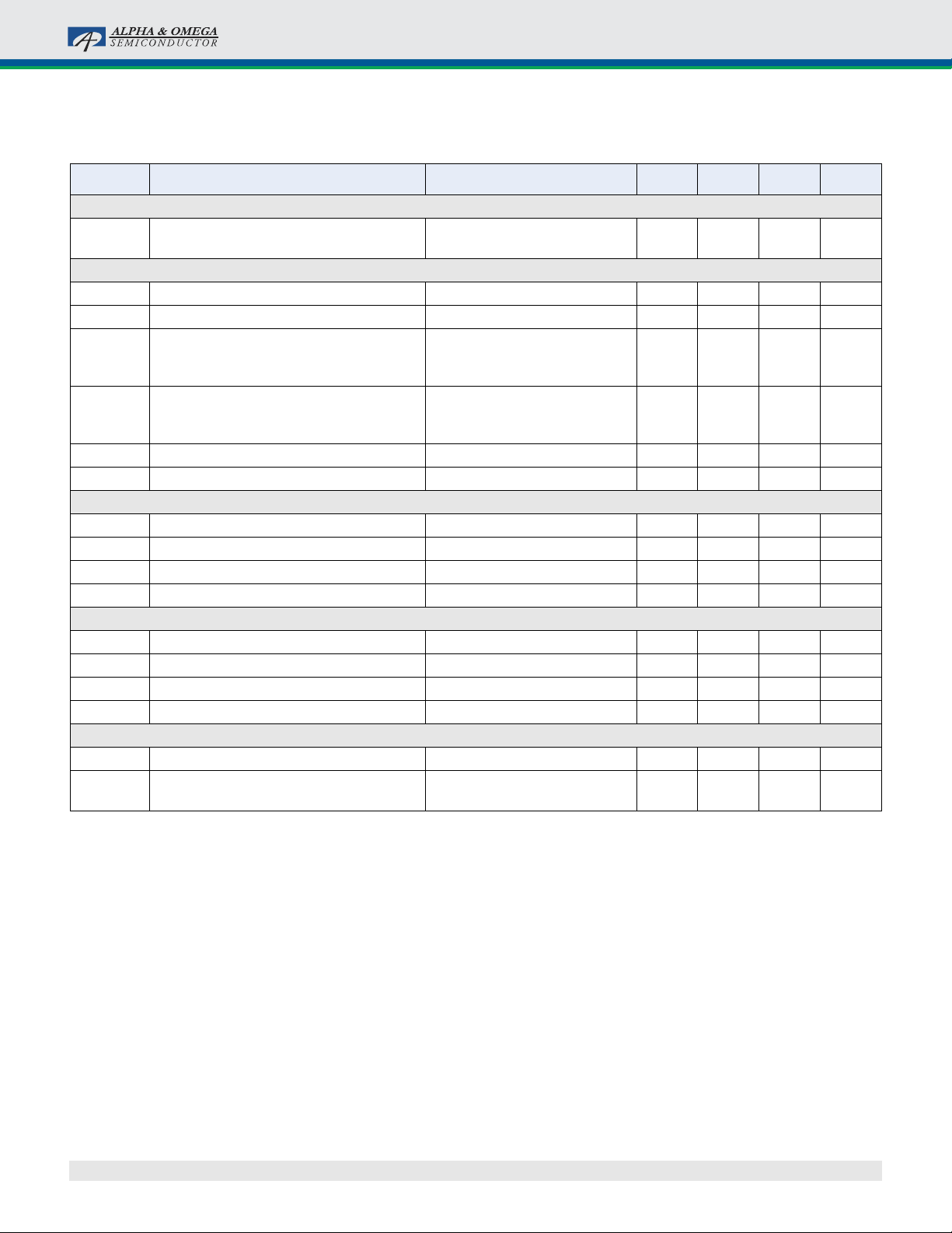
AOZ1237QI-02
Absolute Maximum Ratings
Exceeding the Absolute Maximum Ratings may damage the
device.
Parameter Rating
IN, TON to AGND -0.3V to 30V
LX to AGND -2V to 30V
BST to AGND -0.3V to 36V
SS, PGOOD, FB, EN, VCC, PFM to
AGND
PGND to AGND -0.3V to +0.3V
Junction Temperature (T
Storage Temperature (T
ESD Rating
Note:
1. Devices are inherently ESD sensitive, handling precautions are
required. Human body model rating: 1.5k
2. LX to PGND Transient (t<20ns) ------ -7V to V
(1)
) +150°C
J
) -65°C to +150°C
S
in series with 100pF.
IN
+ 7V.
-0.3V to 6V
2kV
Electrical Characteristics
TA = 25°C, V
-40°C to +85°C.
= 12V, V
IN
= 5V, EN = 5V, unless otherwise specified. Specifications in BOLD indicate a temperature range of
CC
Maximum Operating Ratings
The device is not guaranteed to operate beyond the
Maximum Operating ratings.
Parameter Rating
Supply Voltage (VIN)2.7V
Output Voltage Range 0.8V to 0.85*V
Ambient Temperature (TA) -40°C to +85°C
Package Thermal Resistance
)40°C/W
(θ
JA
) 4.5°C/W
(θ
JC
Note:
3. Connect V
to external 5V for VIN = 2.7V ~ 6.5V application.
CC
(3)
to 24V
IN
Symbol Parameter Conditions Min. Typ. Max Units
V
IN
V
UVLO
I
q
I
OFF
V
FB
I
FB
Enable
V
EN
V
EN_HYS
PFM Control
V
PFM
V
PFMHYS
Modulator
T
ON
T
ON_MIN
T
OFF_MIN
IN Supply Voltage 2.7 24 V
Under-Voltage Lockout Threshold of VCC
Quiescent Supply Current of VCC I
Shutdown Supply Current V
Feedback Voltage
rising
V
CC
falling 3.2
V
CC
= 0, VFB = 1V, V
OUT
= 0V 120A
EN
T
= 25°C
A
TA = 0°C to 85°C
> 2V 11.5mA
EN
0.792
0.788
4.0
3.7
0.800
0.800
4.4
0.808
0.812
V
V
Load Regulation 0.5 %
Line Regulation 1%
FB Input Bias Current 200 nA
EN Input Threshold
Off threshold
On threshold 2.5
0.5
V
EN Input Hysteresis 100 mV
PFM Input Threshold
PFM Mode threshold
Force PWM threshold 2.5
0.5
V
PFM Input Hysteresis 100 mV
On Time
R
= 100k, VIN = 12V
TON
= 100k, VIN = 24V
R
TON
200 250
150
300
ns
Minimum On Time 100 ns
Minimum Off Time 250 400 ns
Rev. 2.0 April 2013
www.aosmd.com
Page 4 of 15
AOZ1237QI-02
Electrical Characteristics
TA = 25°C, V
= 12V, V
IN
= 5V, EN = 5V, unless otherwise specified. Specifications in BOLD indicate a temperature range of
CC
(Continued)
-40°C to +85°C.
Symbol Parameter Conditions Min. Typ. Max Units
Soft-Start
I
SS_OUT
Power Good Signal
V
PG_LOW
V
PGH
V
PGL
T
PG_L
Under Voltage and Over Voltage Protection
V
PL
T
PL
V
PH
T
UV_LX
Power Stage Output
R
DS(ON)
R
DS(ON)
Over-current and Thermal Protection
I
LIM
SS Source Current VSS = 0
C
= 0.001F to 0.1F
SS
PGOOD Low Voltage I
= 1mA 0.5 V
OL
71015A
PGOOD Leakage Current ±1 A
PGOOD Threshold
(Low level to High level)
PGOOD Threshold
(High level to Low level)
FB rising (AOZ1237-02)
FB rising (AOZ1237-04)
FB falling (AOZ1237-04 only)
FB rising (AOZ1237-02/04)
FB falling (AOZ1237-02)
FB falling (AOZ1237-04)
80
85
114
117
77
82
85
90
117
120
82
87
90
95
120
123
87
92
PGOOD Threshold Hysteresis 3 %
PGOOD Fault Delay Time (FB falling) 50 s
Under Voltage Threshold FB falling -30 -25 -20 %
Under Voltage Delay Time 128 s
Over Voltage Threshold FB rising 17 20 23 %
Under Voltage Shutdown Blanking Time VIN = 12V, VEN = 0V, VCC = 5V 20 ms
High-Side NFET On-Resistance VIN = 12V, VCC = 5V 35 45 m
High-Side NFET Leakage V
= 0V, VLX = 0V 10 A
EN
Low-Side NFET On-Resistance VLX = 12V, VCC = 5V 8 12 m
Low-Side NFET Leakage V
= 0V 10 A
EN
Valley Current Limit VCC = 5V 11 A
Thermal Shutdown Threshold
T
J
T
J
rising
falling
145
100
%
%
°C
Rev. 2.0 April 2013
www.aosmd.com
Page 5 of 15
 Loading...