

Alpha & Omega AON7408 Schematic [ru]
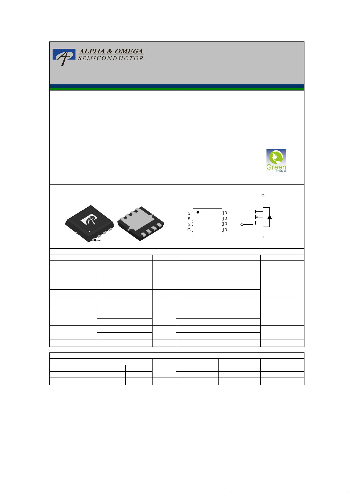
General Description Product Summary
V
Symbol
Absolute Maximum Ratings T
=25°C unless otherwise noted
V
A
V
Drain-Source Voltage
30
A
AON7408
30V N-Channel MOSFET
• The AON7408 uses advanced trench technology and
design to provide excellent R
with low gate charge.
DS(ON)
This device is suitable for use in general purpose
applications.
DS
ID (at VGS=10V) 18A
R
R
(at VGS=10V) < 20mΩ
DS(ON)
(at VGS=4.5V) < 32mΩ
DS(ON)
• RoHS and Halogen-Free Compliant
100% UIS Tested
100% Rg Tested
Top View Bottom View
DFN 3x3 EP
Pin 1
A
Top View
1
2
3
4
8
7
6
5
Maximum UnitsParameter
DS
V
GS
C
B
A
TC=25°C
TC=100°C
TA=25°C
TA=70°C
TC=25°C
TC=100°C
TA=25°C
TA=70°C
I
D
I
DM
I
DSM
P
D
P
DSM
TJ, T
STG
Continuous Drain
B
Current
Pulsed Drain Current
Continuous Drain
A
Current
Power Dissipation
Power Dissipation
Junction and Storage Temperature Range -55 to 150
±20Gate-Source Voltage
18
11.5
64
10
8
11
4.5
3.1
2
30V
D
G
S
V
A
A
W
W
°C
Thermal Characteristics
Parameter Typ Max
Maximum Junction-to-Ambient
Maximum Junction-to-Ambient
Maximum Junction-to-Case
Symbol
t ≤ 10s
Steady-State
B
Steady-State
R
θJA
R
θJC
25
62
8.8
40
75
11
Units
°C/W
°C/W
°C/W
www.aosmd.com Page 1 of 6
t
15.8
ns
Turn-Off DelayTime
R
=3
Ω
Electrical Characteristics (TJ=25°C unless otherwise noted)
AON7408
Symbol Min Typ Max Units
Parameter Conditions
STATIC PARAMETERS
BV
I
DSS
I
GSS
V
GS(th)
I
D(ON)
R
DS(ON)
g
FS
V
SD
I
S
Drain-Source Breakdown Voltage
DSS
Zero Gate Voltage Drain Current
Gate-Body leakage current
Gate Threshold Voltage
On state drain current
Static Drain-Source On-Resistance
Forward Transconductance
Diode Forward Voltage
Maximum Body-Diode Continuous Current
ID=250µA, VGS=0V
30 V
VDS=30V, VGS=0V 1
TJ=55°C 5
VDS=0V, VGS=±20V
VDS=V
GS,ID
=250µA
VGS=10V, VDS=5V
VGS=10V, ID=10A
1.5 2.1 2.6 V
64 A
15.3 20
±100 nA
TJ=125°C 23.3 30
VGS=4.5V, ID=5A
VDS=5V, ID=10A
IS=1A,VGS=0V
22.7 32 mΩ
17 S
0.75 1 V
µA
mΩ
12 A
DYNAMIC PARAMETERS
C
iss
C
oss
C
rss
R
g
Input Capacitance
Output Capacitance
Reverse Transfer Capacitance
Gate resistance
VGS=0V, VDS=15V, f=1MHz
VGS=0V, VDS=0V, f=1MHz
0.6 1.8 2.8 Ω
373 448 pF
67 pF
41 pF
SWITCHING PARAMETERS
Q
g
Q
gs
Q
gd
t
D(on)
t
r
D(off)
t
f
t
rr
Q
rr
A: The value of R
based on T
B. The power dissipation PDis based on T
dissipation limit for cases where additional heatsinking is used.
C: Repetitive rating, pulse width limited by junction temperature T
D. The R
E. The static characteristics in Figures 1 to 6 are obtained using <300 µs pulses, duty cycle 0.5% max.
F. These curves are based on the junction-to-case thermal impedence which is measured with the device mounted to a large heatsink, assuming
a maximum junction temperature of T
G. These tests are performed with the device mounted on 1 in2FR-4 board with 2oz. Copper, in a still air environment with TA=25°C.
H. The maximum current rating is limited by bond-wires.
Total Gate Charge
Gate Source Charge
Gate Drain Charge
Turn-On DelayTime
Turn-On Rise Time
Turn-Off Fall Time
Body Diode Reverse Recovery Time
Body Diode Reverse Recovery Charge
is measured with the device in a still air environment with TA=25°C. The power dissipation P
θJA
=150°C, using t ≤ 10s junction-to-ambient thermal resistance.
J(MAX)
is the sum of the thermal impedence from junction to case R
θJA
=150°C, using junction-to-case thermal resistance, and is more useful in setting the upper
J(MAX)
=150°C. The SOA curve provides a single pulse rating.
J(MAX)
VGS=4.5V, VDS=15V, ID=10A
VGS=10V, VDS=15V, RL=1.5Ω,
GEN
IF=10A, dI/dt=100A/µs
IF=10A, dI/dt=100A/µs
=150°C.
J(MAX)
and case to ambient.
θJC
7.1 8.6 nC
1.2 nC
1.6 nC
4.3 ns
2.8 ns
3 ns
10.5 12.6 ns
4.5
and current rating I
DSM
nC
DSM
are
Rev.8.0: November 2013 www.aosmd.com Page 2 of 6
THIS PRODUCT HAS BEEN DESIGNED AND QUALIFIED FOR THE CONSUMER MARKET. APPLICATIONS OR USES AS CRITICAL
COMPONENTS IN LIFE SUPPORT DEVICES OR SYSTEMS ARE NOT AUTHORIZED. AOS DOES NOT ASSUME ANY LIABILITY ARISING
OUT OF SUCH APPLICATIONS OR USES OF ITS PRODUCTS. AOS RESERVES THE RIGHT TO IMPROVE PRODUCT DESIGN,
FUNCTIONS AND RELIABILITY WITHOUT NOTICE.
TYPICAL ELECTRICAL AND THERMAL CHARACTERISTICS
125°C
6V
AON7408
60
10V
50
40
30
(A)
D
I
20
10
0
0 1 2 3 4 5
Fig 1: On-Region Characteristics
40
35
30
Ω
Ω)
Ω
Ω
(m
25
DS(ON)
R
20
15
10
0 5 10 15 20
Figure 3: On-Resistance vs. Drain Current and Gate
VDS(Volts)
VGS=4.5V
VGS=10V
ID(A)
Voltage
4.5V
VGS=3.5V
15
VDS=5V
12
9
(A)
D
I
6
3
0
1.5 2 2.5 3 3.5 4 4.5
Figure 2: Transfer Characteristics
1.8
1.6
1.4
1.2
1
Normalized On-Resistance
0.8
0 25 50 75 100 125 150 175
VGS(Volts)
VGS=10V
Figure 4: On-Resistance vs. Junction Temperature
25°C
VGS=4.5V
Temperature (°C)
17
5
2
10
0
18
60
50
40
Ω
Ω)
Ω
Ω
(m
30
DS(ON)
R
20
10
2 4 6 8 10
Figure 5: On-Resistance vs. Gate-Source Voltage
125°C
25°C
VGS(Volts)
ID=10A
1.0E+01
1.0E+00
1.0E-01
(A)
1.0E-02
S
I
1.0E-03
1.0E-04
1.0E-05
40
125°C
25°C
0.0 0.2 0.4 0.6 0.8 1.0 1.2
Figure 6: Body-Diode Characteristics
VSD(Volts)
Rev.8.0: November 2013 www.aosmd.com Page 3 of 6
 Loading...