

Alpha & Omega AON6970 Schematic [ru]
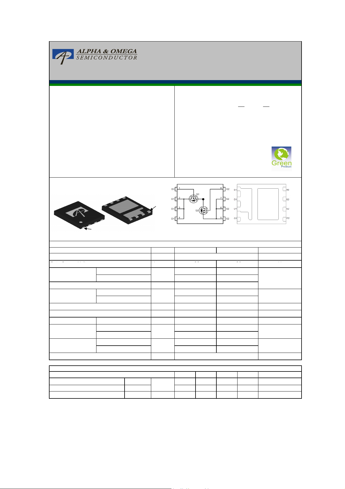
AON6970
30V Dual Asymmetric N-Channel AlphaMOS
Q1
Q2
Symbol
Absolute Maximum Ratings T
=25°C unless otherwise noted
V
A D
Gate-Source Voltage
V66±20±20
General Description Product Summary
• Latest Trench Power AlphaMOS (αMOS LV) technology
• Very Low RDS(on) at 4.5V
GS
• Low Gate Charge
• High Current Capability
• RoHS and Halogen-Free Compliant
Application 100% Rg Tested
• DC/DC Converters in Computing, Servers, and POL
• Isolated DC/DC Converters in Telecom and Industrial
V
DS
ID (at VGS=10V) 58A 85A
R
R
(at VGS=10V) <5.4mΩ <1.5mΩ
DS(ON)
(at VGS=4.5V) <8.5mΩ <2.3mΩ
DS(ON)
100% UIS Tested
30V 30V
DFN5X6D
Top View Bottom View
PIN1
G2
S2
S2
S2
PHASE
(S1/D2)
A
D1
D1
PIN1
G1
D1
D1
Top View
PHASE
S1/D2
Q2: SRFET
Soft Recovery MOSFET:
Integrated Schottky Diode
TM
Max Q1Parameter
Drain-Source Voltage
Continuous Drain
Current
Pulsed Drain Current
Continuous Drain
Current
Avalanche Current
Avalanche Energy L=0.05mH
TC=25°C
TC=100°C
C
TA=25°C
TA=70°C
C
C
VDS Spike V
TC=25°C
B
Power Dissipation
TC=100°C
TA=25°C
A
Power Dissipation
TA=70°C
Junction and Storage Temperature Range -55 to 150
V
DS
GS
I
D
I
DM
I
DSM
I
AS
E
AS
SPIKE
P
D
P
DSM
TJ, T
30
58 85
36
135
24
19
35
31 106
36 36
31
12
5 4.1
3.2 2.6
STG
Bottom View
D1 S1/D2
Max Q2 Units
V
A
340
42
33
65
A
A
mJ
V 100ns
78
31
W
W
°C
Thermal Characteristics
Parameter Symbol Typ Q1 Typ Q2 Max Q1 Max Q2
Maximum Junction-to-Ambient
Maximum Junction-to-Ambient
Maximum Junction-to-Case
Rev0 : Sep 2012 www.aosmd.com Page 1 of 10
A
t ≤ 10s
Steady-State
Steady-State
Units
R
θJA
R
θJC
20 25 25 30
50 56 60 67
3.3 1.2 4 1.6
°C/W
°C/W
°C/W
t
17
ns
R
=3
Ω
Turn-Off DelayTime
Q1 Electrical Characteristics (TJ=25°C unless otherwise noted)
AON6970
Symbol Min Typ Max Units
Parameter Conditions
STATIC PARAMETERS
BV
I
DSS
I
GSS
V
GS(th)
R
DS(ON)
g
FS
V
SD
I
S
Drain-Source Breakdown Voltage
DSS
Zero Gate Voltage Drain Current
Gate-Body leakage current
Gate Threshold Voltage
Static Drain-Source On-Resistance
Forward Transconductance
Diode Forward Voltage
Maximum Body-Diode Continuous Current
ID=250µA, VGS=0V
30 V
VDS=30V, VGS=0V 1
TJ=55°C 5
VDS=0V, VGS= ±20V
VDS=V
GS ID
=250µA
VGS=10V, ID=20A
1.3 1.8 2.3 V
±100 nA
4.4 5.4
TJ=125°C 6.8 8.3
VGS=4.5V, ID=20A
VDS=5V, ID=20A
IS=1A,VGS=0V
6.7 8.5 mΩ
80 S
0.7 1 V
35 A
µA
mΩ
DYNAMIC PARAMETERS
C
iss
C
oss
C
rss
R
g
Input Capacitance
Output Capacitance
Reverse Transfer Capacitance
Gate resistance
VGS=0V, VDS=15V, f=1MHz
VGS=0V, VDS=0V, f=1MHz
1171 pF
284 pF
59 pF
0.3 0.6 0.9 Ω
SWITCHING PARAMETERS
Qg(10V) 17 23 nC
Qg(4.5V) 8 11 nC
Q
gs
Q
gd
t
D(on)
t
r
D(off)
t
f
t
rr
Q
rr
A. The value of R
Power dissipation P
depends on the user's specific board design.
B. The power dissipation PDis based on T
dissipation limit for cases where additional heatsinking is used.
C. Repetitive rating, pulse width limited by junction temperature T
initial TJ=25°C.
D. The R
E. The static characteristics in Figures 1 to 6 are obtained using <300µs pulses, duty cycle 0.5% max.
F. These curves are based on the junction-to-case thermal impedence which is measured with the device mounted to a large heatsink, assuming
a maximum junction temperature of T
G. The maximum current rating is limited by package.
H. These tests are performed with the device mounted on 1 in2FR-4 board with 2oz. Copper, in a still air environment with TA=25°C.
Total Gate Charge
Total Gate Charge
Gate Source Charge
Gate Drain Charge
Turn-On DelayTime
Turn-On Rise Time
Turn-Off Fall Time
Body Diode Reverse Recovery Time
Body Diode Reverse Recovery Charge
is measured with the device mounted on 1in2FR-4 board with 2oz. Copper, in a still air environment with TA=25°C. The
θJA
is based on R
DSM
is the sum of the thermal impedence from junction to case R
θJA
t ≤ 10s and the maximum allowed junction temperature of 150°C. The value in any given application
θJA
=150°C, using junction-to-case thermal resistance, and is more useful in setting the upper
J(MAX)
=150°C. The SOA curve provides a single pulse rating.
J(MAX)
VGS=10V, VDS=15V, ID=20A
4.7 nC
2 nC
6.5 ns
VGS=10V, VDS=15V, RL=0.75Ω,
GEN
15.5 ns
2.5 ns
IF=20A, dI/dt=500A/µs
IF=20A, dI/dt=500A/µs
=150°C. Ratings are based on low frequency and duty cycles to keep
J(MAX)
and case to ambient.
θJC
12.3
22.5 nC
ns
Rev0 : Sep 2012 www.aosmd.com Page 2 of 10
COMPONENTS IN LIFE SUPPORT DEVICES OR SYSTEMS ARE NOT AUTHORIZED. AOS DOES NOT ASSUME ANY LIABILITY ARISING
OUT OF SUCH APPLICATIONS OR USES OF ITS PRODUCTS. AOS RESERVES THE RIGHT TO IMPROVE PRODUCT DESIGN,
FUNCTIONS AND RELIABILITY WITHOUT NOTICE.
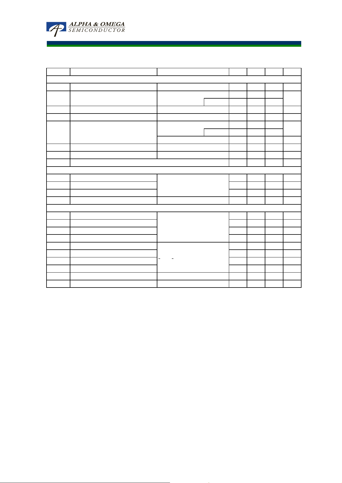
Q1-CHANNEL: TYPICAL ELECTRICAL AND THERMAL CHARACTERISTICS
Voltage (Note E)
125°C
Voltage (Note E)
125°C
(Note E)
AON6970
100
10V
80
4.5V
6V
60
(A)
D
I
40
20
VGS=3.0V
0
0 1 2 3 4 5
Fig 1: On-Region Characteristics (Note E)
VDS(Volts)
10
8
Ω
Ω)
Ω
Ω
6
(m
4
DS(ON)
R
VGS=4.5V
VGS=10V
2
0
0 5 10 15 20 25 30
Figure 3: On-Resistance vs. Drain Current and Gate
ID(A)
3.5V
4V
100
VDS=5V
80
60
(A)
D
I
40
25°C
20
0
0 1 2 3 4 5 6
Figure 2: Transfer Characteristics (Note E)
VGS(Volts)
1.8
1.6
VGS=10V
I
=20A
1.4
1.2
VGS=4.5V
1
Normalized On-Resistance
ID=20A
0.8
0 25 50 75 100 125 150 175
Figure 4: On-Resistance vs. Junction Temperature
Temperature (°C)
14
12
10
Ω
Ω)
Ω
Ω
8
(m
6
DS(ON)
R
4
2
25°C
25°C
0
2 4 6 8 10
Figure 5: On-Resistance vs. Gate-Source Voltage
VGS(Volts)
(Note E)
ID=20A
ID=11.5A
125°C
1.0E+02
1.0E+01
1.0E+00
1.0E-01
(A)
S
I
1.0E-02
1.0E-03
1.0E-04
1.0E-05
125°C
25°C
0.0 0.2 0.4 0.6 0.8 1.0 1.2
Figure 6: Body-Diode Characteristics (Note E)
VSD(Volts)
Rev0 : Sep 2012 www.aosmd.com Page 3 of 10
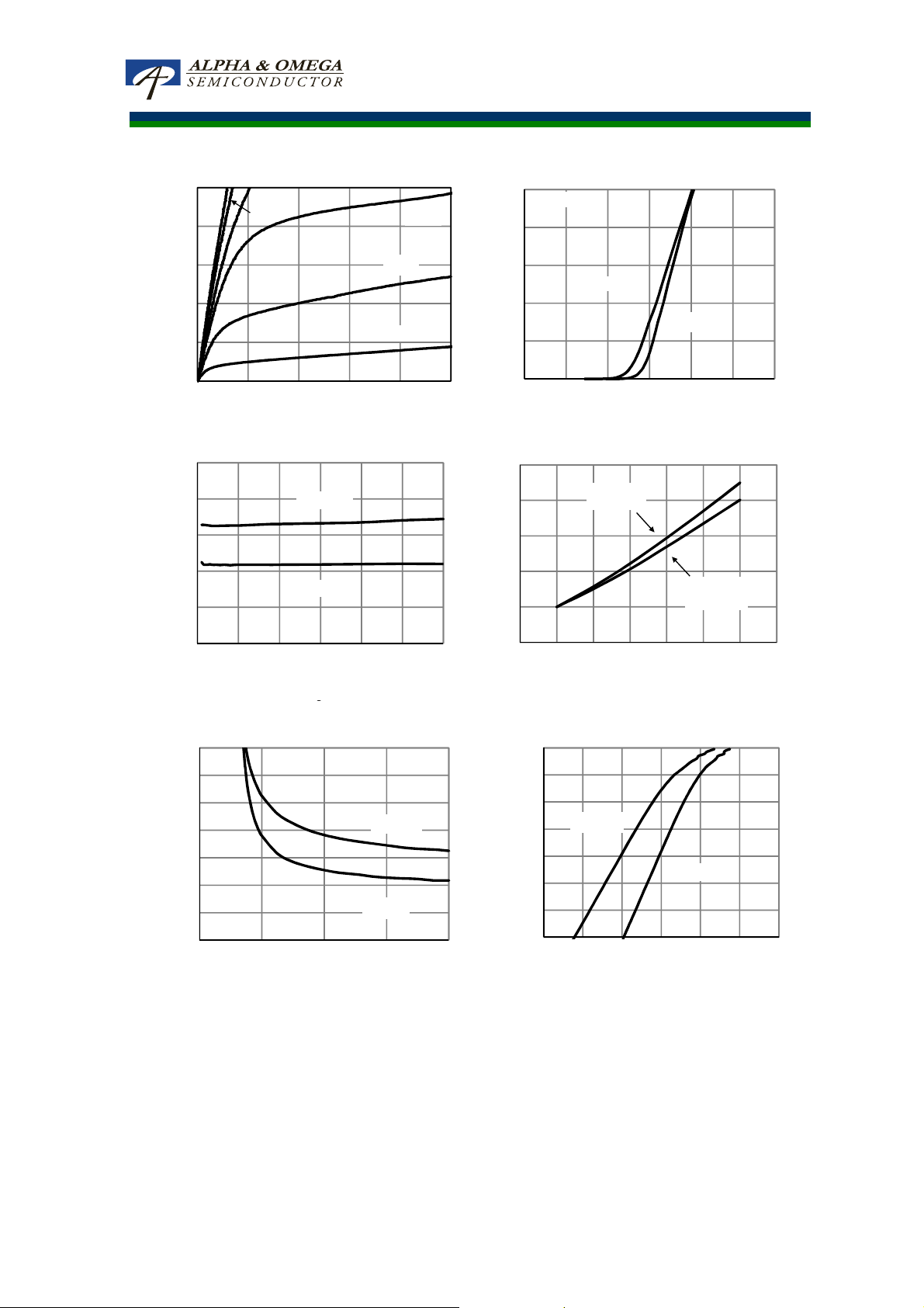
Q1-CHANNEL: TYPICAL ELECTRICAL AND THERMAL CHARACTERISTICS
10µs
Figure 10: Single Pulse Power Rating Junction
-to-
Figure 9: Maximum Forward Biased
Figure 10: Single Pulse Power Rating Junction
-to-
T
T
P
AON6970
10
VDS=15V
ID=20A
8
6
(Volts)
GS
4
V
2
0
0 5 10 15 20
Figure 7: Gate-Charge Characteristics
Qg(nC)
1000.0
100.0
R
DS(ON)
limited
10.0
(Amps)
1.0
D
I
0.1
T
=150°C
J(Max)
TC=25°C
DC
0.0
0.01 0.1 1 10 100
VDS(Volts)
Safe Operating Area (Note F)
100us
1ms
10ms
1600
1400
1200
C
iss
1000
800
600
Capacitance (pF)
400
C
200
rss
C
oss
0
0 5 10 15 20 25 30
Figure 8: Capacitance Characteristics
200
160
VDS(Volts)
T
=150°C
J(Max)
TC=25°C
120
80
Power (W)
40
0
0.0001 0.001 0.01 0.1 1 10
Pulse Width (s)
Case (Note F)
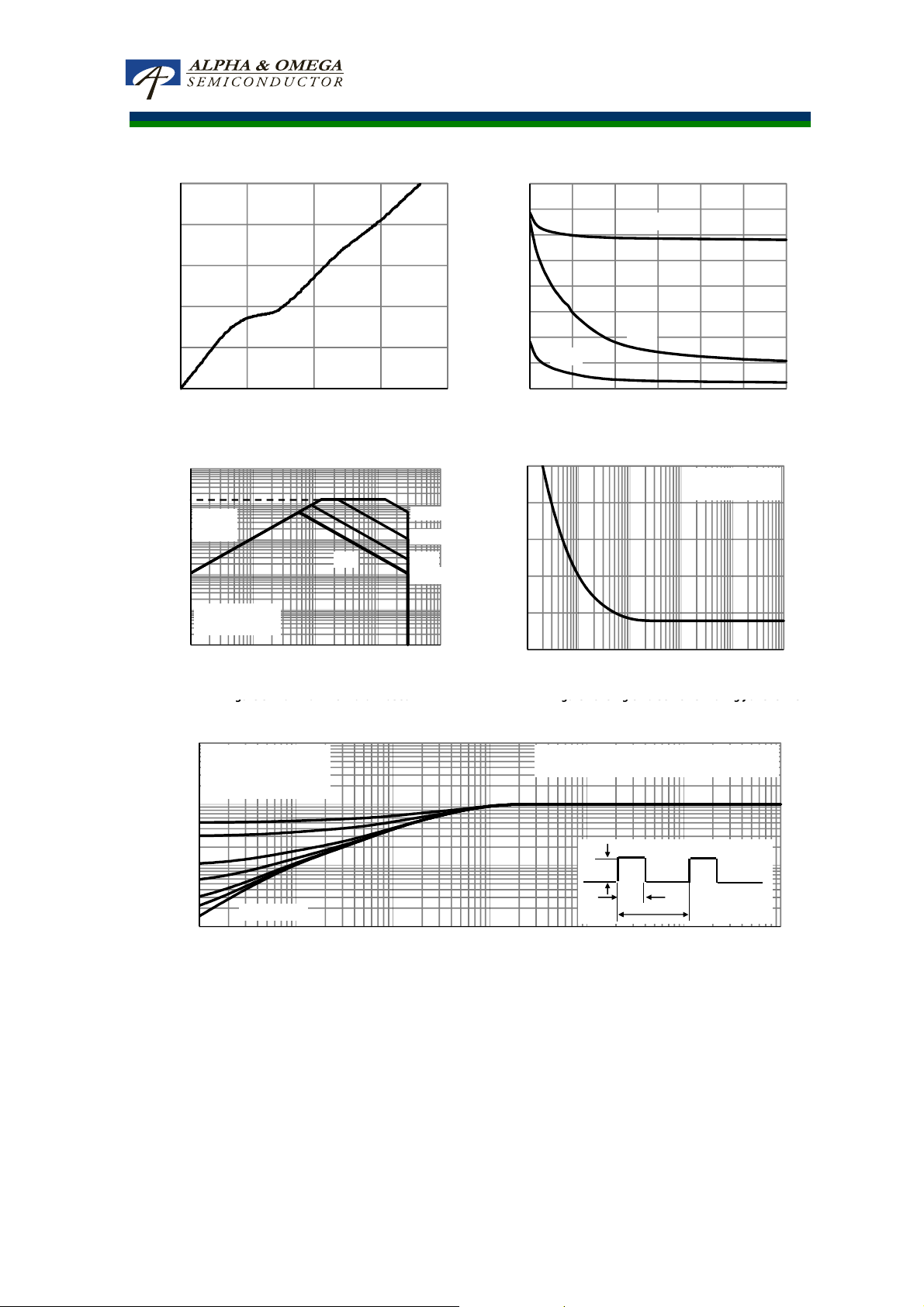
10
D=Ton/T
T
J,PK=TC+PDM.ZθJC.RθJC
R
=4°C/W
θJC
1
0.1
Normalized Transient
Thermal Resistance
θ
θJC
θ
θ
Z
In descending order
D=0.5, 0.3, 0.1, 0.05, 0.02, 0.01, single pulse
Single Pulse
0.01
0.00001 0.0001 0.001 0.01 0.1 1 10
Pulse Width (s)
Figure 11: Normalized Maximum Transient Thermal Impedance (Note F)
Rev0 : Sep 2012 www.aosmd.com Page 4 of 10
 Loading...