

Alpha & Omega AO3423L Schematic [ru]
General Description Product Summary
VDS-20V
Typical ESD protection
HBM Class 2
Symbol
V
Drain-Source Voltage
-20
V
Absolute Maximum Ratings T
=25°C unless otherwise noted
V
DS
A
Drain-Source Voltage
-20
V
A D
The AO3423 uses advanced trench technology to provide
excellent R
voltages as low as 2.5V. This device is suitable for use as
a load switch applications.
, low gate charge and operation with gate
DS(ON)
ID (at VGS=-10V) -2A
R
R
R
(at VGS= -10V) < 92mΩ
DS(ON)
(at VGS= -4.5V) < 118mΩ
DS(ON)
(at VGS= -2.5V) < 166mΩ
DS(ON)
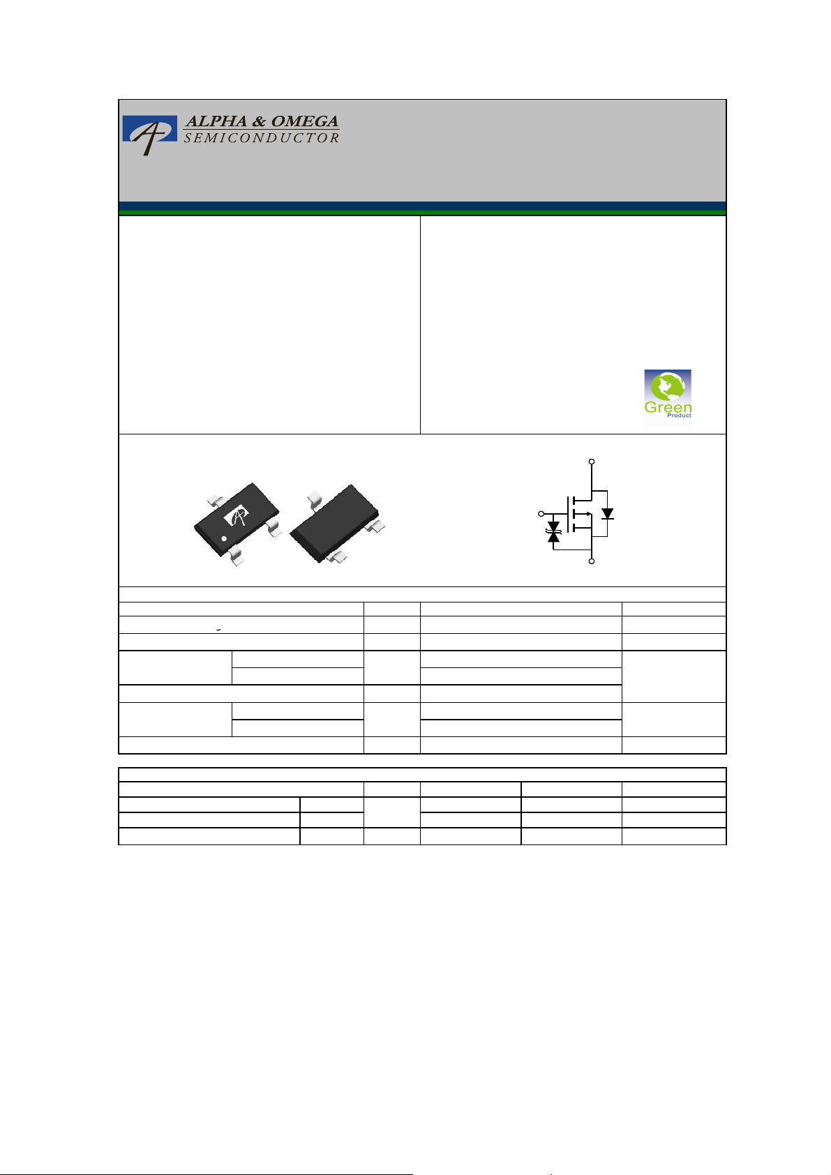
AO3423
20V P-Channel MOSFET
Top View Bottom View
D
SOT23
D
S
G
A
G
S
G
Maximum UnitsParameter
V
GS
Continuous Drain
Current
Pulsed Drain Current
TA=25°C
TA=70°C
C
TA=25°C
B
Power Dissipation
TA=70°C
Junction and Storage Temperature Range
I
D
I
DM
P
D
TJ, T
STG
-2
-2
-17
1.4
0.9
-55 to 150 °C
Thermal Characteristics
Parameter Typ Max
Maximum Junction-to-Ambient
Maximum Junction-to-Ambient
Maximum Junction-to-Lead
t ≤ 10s
Steady-State
Steady-State
Symbol
R
θJA
R
θJL
65
85
43
90
125
60
D
S
V±12Gate-Source Voltage
A
W
Units
°C/W
°C/W
°C/W
www.aosmd.com Page 1 of 5
tr5.5
ns
Turn-On Rise Time
VGS=-10V, V
=-10V, R
=5Ω,
Electrical Characteristics (TJ=25°C unless otherwise noted)
AO3423
Symbol Min Typ Max Units
Parameter Conditions
STATIC PARAMETERS
BV
I
DSS
I
GSS
V
GS(th)
I
D(ON)
R
DS(ON)
g
FS
V
SD
I
S
Drain-Source Breakdown Voltage
DSS
Zero Gate Voltage Drain Current
Gate-Body leakage current
Gate Threshold Voltage
On state drain current
Static Drain-Source On-Resistance
Forward Transconductance
Diode Forward Voltage
Maximum Body-Diode Continuous Current
ID=-250µA, VGS=0V
-20 V
VDS=-20V, VGS=0V -1
TJ=55°C -5
VDS=0V, VGS= ±12V
VDS=VGS, ID=-250µΑ
VGS=-4.5V, VDS=-5V
VGS=-10V, ID=-2A
-0.5 -0.85 -1.2 V
-17 A
±10 µA
76 92
TJ=125°C 99 119
VGS=-4.5V, ID=-2A
VGS=-2.5V, ID=-1A
VDS=-5V, ID=-2A
IS=-1A,VGS=0V
94 118 mΩ
128 166 mΩ
6.8 S
-0.76 -1 V
-1.5 A
µA
mΩ
DYNAMIC PARAMETERS
C
iss
C
oss
C
rss
R
g
Input Capacitance
Output Capacitance
Reverse Transfer Capacitance
Gate resistance
VGS=0V, VDS=-10V, f=1MHz
VGS=0V, VDS=0V, f=1MHz
250 325 400 pF
40 63 85 pF
22 37 52 pF
11.2 17 Ω
SWITCHING PARAMETERS
Q
g
Q
gs
Q
gd
t
D(on)
t
D(off)
t
f
t
rr
Q
rr
A. The value of R
value in any given application depends on the user's specific board design.
B. The power dissipation PDis based on T
C. Repetitive rating, pulse width limited by junction temperature T
initialTJ=25°C.
D. The R
E. The static characteristics in Figures 1 to 6 are obtained using <300µs pulses, duty cycle 0.5% max.
F. These curves are based on the junction-to-ambient thermal impedance which is measured with the device mounted on 1in2FR-4 board with
2oz. Copper, assuming a maximum junction temperature of T
Total Gate Charge
Gate Source Charge
Gate Drain Charge
Turn-On DelayTime
Turn-Off DelayTime
Turn-Off Fall Time
Body Diode Reverse Recovery Time
Body Diode Reverse Recovery Charge
is measured with the device mounted on 1in2FR-4 board with 2oz. Copper, in a still air environment with TA=25°C. The
θJA
=150°C, using ≤ 10s junction-to-ambient thermal resistance.
J(MAX)
is the sum of the thermal impedance from junction to lead R
θJA
J(MAX)
3.2
VGS=-4.5V, VDS=-10V, ID=-2A
0.6
0.9
11
DS
R
=3Ω
GEN
IF=-2A, dI/dt=100A/µs
IF=-2A, dI/dt=100A/µs
=150°C. Ratings are based on low frequency and duty cycles to keep
J(MAX)
and lead to ambient.
θJL
=150°C. The SOA curve provides a single pulse rating.
L
22
6.1
1.4 nC
8
4.5 nC
nC
nC
ns
ns
ns
ns
Rev 5: Nov 2011 www.aosmd.com Page 2 of 5
COMPONENTS IN LIFE SUPPORT DEVICES OR SYSTEMS ARE NOT AUTHORIZED. AOS DOES NOT ASSUME ANY LIABILITY ARISING
OUT OF SUCH APPLICATIONS OR USES OF ITS PRODUCTS. AOS RESERVES THE RIGHT TO IMPROVE PRODUCT DESIGN,
FUNCTIONS AND RELIABILITY WITHOUT NOTICE.
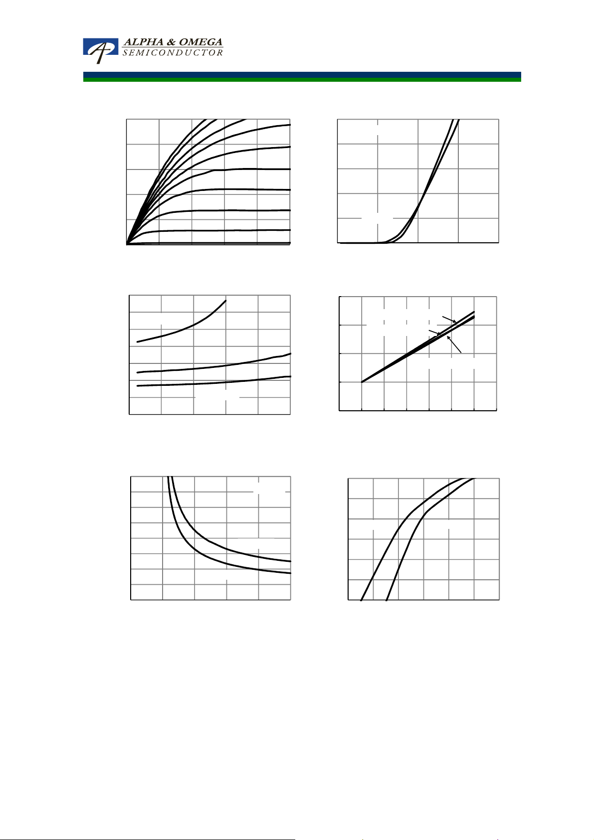
TYPICAL ELECTRICAL AND THERMAL CHARACTERISTICS
-
4V
Voltage (Note E)
25°C
125°C
(Note E)
AO3423
25
-6V
-8V
20
-5V
15
(A)
D
-I
10
5
0
VGS=-1.5V
0 1 2 3 4 5
Fig 1: On-Region Characteristics (Note E)
-VDS(Volts)
180
160
VGS=-2.5V
140
Ω
Ω)
Ω
Ω
120
(m
100
DS(ON)
R
VGS=-4.5V
80
60
VGS=-10V
40
0 2 4 6 8 10
Figure 3: On-Resistance vs. Drain Current and Gate
-ID(A)
-2.5V
-2V
-3.5V
-3V
10
VDS=-5V
8
6
(A)
D
-I
4
2
125°C
25°C
0
0 1 2 3 4
Figure 2: Transfer Characteristics (Note E)
-VGS(Volts)
1.6
ID=-2A, VGS=-4.5V
1.4
ID=-2A, VGS=-10V
1.2
ID=-1A, VGS=-2.5V
1.0
Normalized On-Resistance
0.8
0 25 50 75 100 125 150 175
Figure 4: On-Resistance vs. Junction Temperature
Temperature (°C)
200
180
160
140
Ω
Ω)
Ω
Ω
(m
120
DS(ON)
100
R
80
25°C
60
40
0 2 4 6 8 10
Figure 5: On-Resistance vs. Gate-Source Voltage
-VGS(Volts)
(Note E)
125°C
ID=-2A
1.0E+01
1.0E+00
1.0E-01
(A)
1.0E-02
S
-I
1.0E-03
1.0E-04
1.0E-05
0.0 0.2 0.4 0.6 0.8 1.0 1.2
Figure 6: Body-Diode Characteristics (Note E)
-VSD(Volts)
Rev 5: Nov 2011 www.aosmd.com Page 3 of 5
 Loading...