ALPHA AV850M1-00 Datasheet

Alpha Industries, Inc. [781] 935-5150 • Fax [617] 824-4579 • Email sales@alphaind.com • www.alphaind.com 1
Specifications subject to change without notice. 2/00A
18–50 GHz GaAs MMIC
Voltage Variable Attenuator
Features
■ Single Voltage Control
■ 40 dB Attenuation Range
■ Balanced 0.25 µm MESFET
Non-Reflective Design
■ 100% On-Wafer RF and DC Testing
■ 100% Visual Inspection to MIL-STD-883
MT 2010
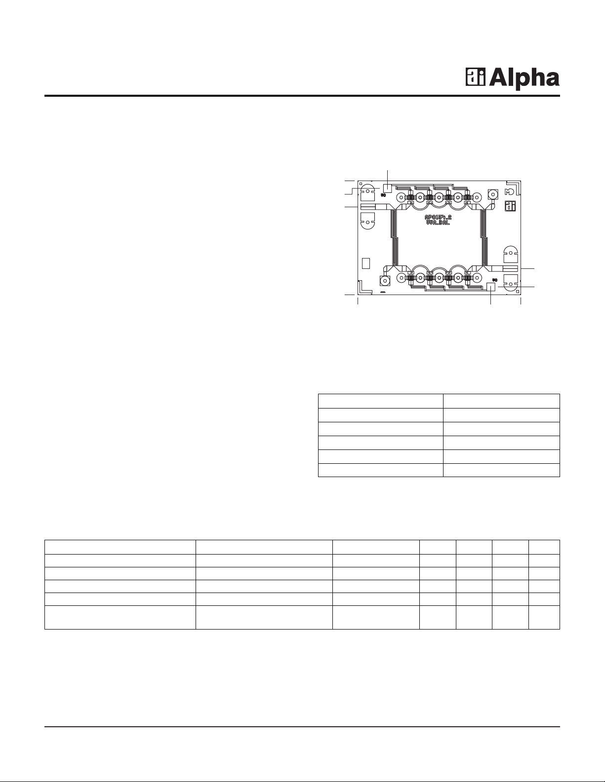
Chip Outline
AV850M1-00
Description
Alpha’s AV850M1-00 MMIC voltage variable attenuator is
a balanced configuration incorporating Lange couplers at
input and output. The attenuator has a typical insertion loss
of 2.5 dB over the 18–40 GHz band with a worst-case
insertion loss of 3.5 dB across the full 18–50 GHz band.
The attenuation range is 35 dB over the full 18–50 GHz
band while typical I/P and O/P return loss is better than
13 dB for all attenuation states. The chip uses Alpha’s
proven 0.25 µm MESFET technology and is based upon
MBE layers and electron beam lithography for the highest
uniformity and repeatability. The MMICs employ surface
passivation to ensure a rugged, reliable part with
through-substrate via holes and gold-based backside
metallization to facilitate a conductive epoxy die attach
process. All chips are screened for insertion loss, full
attenuation and I/P and O/P match over the 18–50 GHz
band for guaranteed performance.
Parameter Condition Symbol Min. Typ.
2
Max. Unit
Maximum Attenuation VC= 0 V ISO 35 45 dB
Minimum Attenuation VC= -5 V I
L
2.5 3.5 dB
Input Return Loss At Min. and Max. Attenuation RL
I
-20 -12.5 dB
Output Return Loss At Min. and Max. Attenuation RL
O
-20 -12.5 dB
Input Power at 1 dB Gain Compression P
1 dB
0 dBm
(For All Attenuation Levels)
1
Electrical Specifications at 25°C (Frequency = 18, 24, 31, 38, 43, 50 GHz)
0.000
0.000
1.634
0.095
0.320
2.000
1.080
1.400
0.365
1.305
Dimensions indicated in mm.
All DC (V) pads are 0.1 x 0.1 mm and RF In, Out pads are 0.07 mm wide.
Chip thickness = 0.1 mm.
Characteristic Value
Operating Temperature (TC) -55°C to +90°C
Storage Temperature (TST) -65°C to +150°C
Control Voltage (VC)-7 V
DC
Power In (PIN) 30 dBm
Junction Temperature (TJ) 175°C
Absolute Maximum Ratings
1. Not measured on a 100% basis.
2. Typical represents the median parameter value across the specified
frequency range for the median chip.

18–50 GHz GaAs MMIC Voltage Variable Attenuator AV850M1-00
2 Alpha Industries, Inc. [781] 935-5150 • Fax [617] 824-4579 • Email sales@alphaind.com • www.alphaind.com
Specifications subject to change without notice. 2/00A
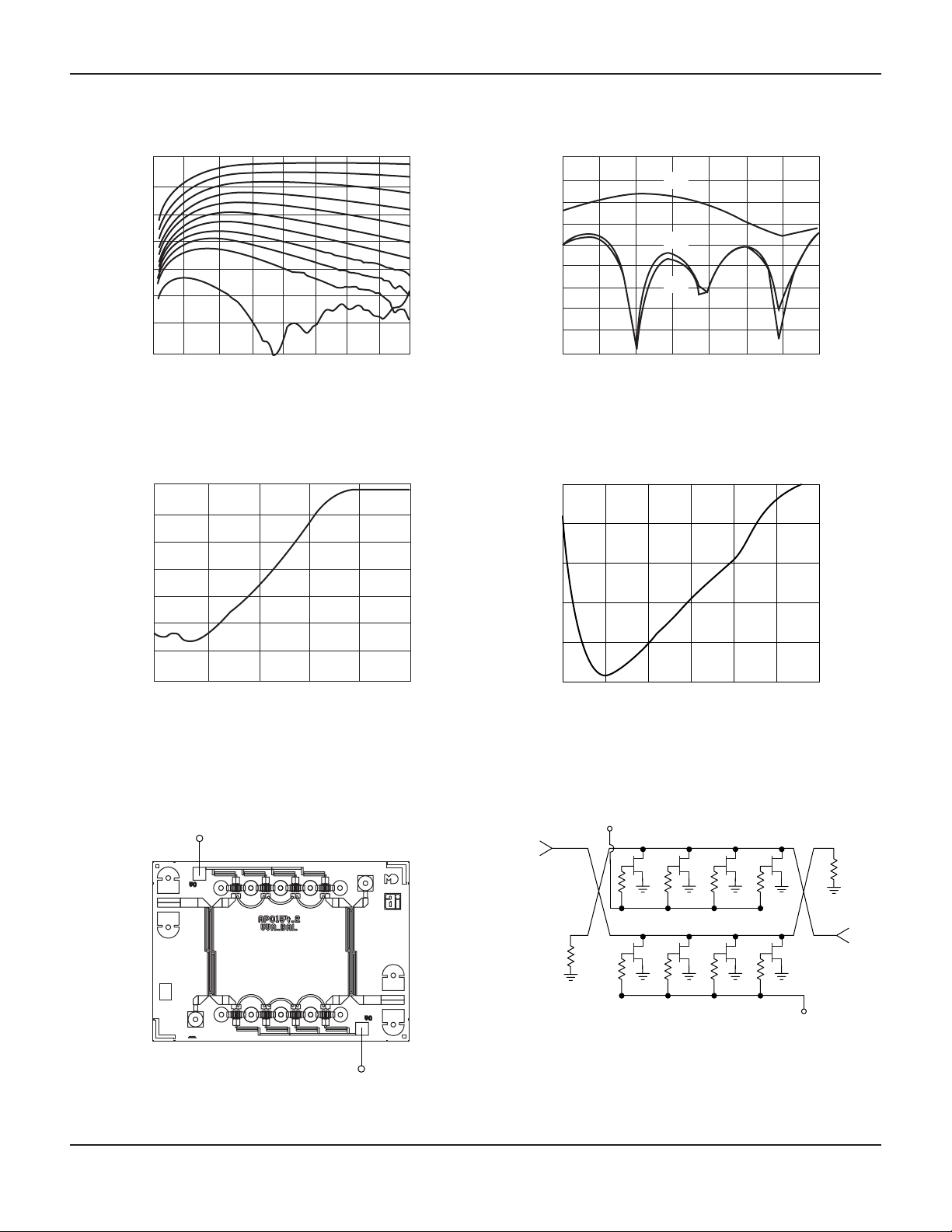
Attenuation vs. Frequency (By State)
Frequency (GHz)
-70
05
Max.
Min.
10 15 20 25 30 35 40
-60
-50
-40
-30
-20
-10
Attenuation (dB)
0
Attenuation vs. Control Voltage
Voltage (V)
-70
0 0.5 1.0 1.5 2.0 2.5
-60
-50
-40
-30
-20
-10
Attenuation (dB)
0
Insertion Loss vs. Frequency
Frequency (GHz)
-9
-7
-8
18 23 28 33 38 43 48 50
-6
-5
-4
-3
-2
-1
Insertion Loss (dB)
Return Loss (dB)
0
-45
-35
-40
-30
-25
-20
-15
-10
-5
0
S
21
S
22
S
11
15 20 25 301050
15
10
5
0
-5
Attenuation (dB)
Attenuation vs. 1.0 dB Compression Point
P
IN
at 1.0 dB Compression (dBm)
20
F = 30 GHz
Typical Performance Data
RF
V
C
V
C
RF
Bias Arrangement
RF IN
RF OUT
V
C
V
C
Circuit Schematic
Bias must be applied to both VC. Voltage range is V
Low
= 0 V to V
High
= -5 V.
V
Low
corresponds to high attenuation state.
 Loading...