ALPHA AL108-338 Datasheet

Alpha Industries, Inc. [978] 241-7000 • Fax [978] 241-7906 • Email sales@alphaind.com • www.alphaind.com 1
Specifications subject to change without notice. 1/02A
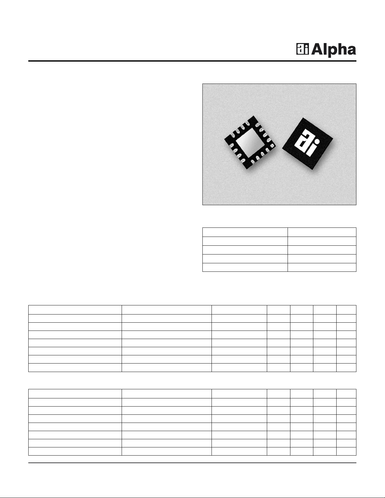
GaAs PHEMT Switchable Gain LNA
Features
■ For 3.2–3.8 GHz Fixed
Wireless Applications
■ Adjustable Gain
■ +7 dBm Output Power
■ +17 dBm Output IP3
■ 2.7 dB Noise Figure
■ Single +5 V Supply
■ Input and Output Matched to 50 Ω
AL108-338
Description
The AL108-338 is an LNA designed for use in
3.2–3.8 GHz WLAN applications. The leadless surface
mount package houses a GaAs PHEMT MMIC that yields
low noise, good 50 Ω match, high gain and powerful
P
1 dB
performance. Powered by a single 5 V supply, it
also offers a 10 dB gain adjustment range.
Parameter Condition Frequency Min. Typ. Max. Unit
Gain 19 21 dB
Output P
-1 dB
6 dBm
Output IP3 PIN= -30 dBm 18 19 dBm
Noise Figure 2.5 2.9 dB
Reverse Isolation 30 40 dB
Input VSWR 50 Ω System 1.5:1 2.0:1
Output VSWR 50 Ω System 1.5:1 2.0:1
Electrical Specifications at 25°C (3.2–3.8 GHz)
Control Voltage = 0 V, Bias Voltage = 5 V, ID= 85 mA
Parameter Condition Frequency Min. Typ. Max. Unit
Gain 810 dB
Output P
-1 dB
6 dBm
Output IP3 PIN= -30 dBm 20 23 dBm
Noise Figure 910dB
Reverse Isolation 30 40 dB
Input VSWR 50 Ω System 1.5:1 2.0:1
Output VSWR 50 Ω System 1.5:1 2.0:1
Control Voltage = 5 V, Bias Voltage = 5 V, ID= 85 mA
Preliminary
Characteristic Value
RF Input Power 20 dBm
Bias Voltage 6 V Max.
Storage Temperature -40 to +85°C
Operating Temperature -65 to +150°C
Absolute Maximum Ratings

GaAs PHEMT Switchable Gain LNA AL108-338
2 Alpha Industries, Inc. [978] 241-7000 • Fax [978] 241-7906 • Email sales@alphaind.com • www.alphaind.com
Specifications subject to change without notice. 1/02A
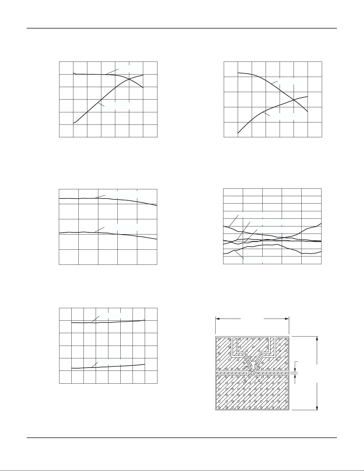
Gain and Output Power
(Low Gain mode)
-15
-10
-5
0
5
10
15
-25 -20 -15 -10 -5 0 5 10
PIN (dBm)
Gain (dB),P
OUT
(dBm)
P
OUT
(dBm)
Gain (Low)
Gain vs. Frequency
Frequency (GHz)
Gain (dB)
0
5
10
15
20
25
3.0 3.2 3.4 3.6 3.8 4.0
High Gain State
Low Gain State
Noise Figure vs. Frequency
Frequency (GHz)
NF (dB)
0
2
4
6
8
10
12
3.1 3.2 3.3 3.4 3.5 3.6 3.7 3.8 3.9
High Gain
Low Gain
VSWR vs. Frequency
Frequency (GHz)
VSWR
1.0
1.1
1.2
1.3
1.4
1.5
1.6
1.7
1.8
1.9
2.0
3.0 3.2 3.4 3.6 3.8 4.0
Input (High Gain)
Output (High Gain)
Input (Low Gain)
Output (Low Gain)
Gain and Output Power
(High Gain mode)
-25 -20 -15 -10 -5 0 5 10
PIN (dBm)
Gain (dB),P
OUT
(dBm)
0
5
10
15
20
25
P
OUT
(dBm)
Gain (High)
Typical Performance Data at 25°C
0.850
0.850
RF
Input
RF
Output
Voltage
Control
Bias
Voltage
0.018
Evaluation Board
Dimensions in inches.
 Loading...