ALPHA AFP02N8-213, AFP02N8-212 Datasheet

Alpha Industries, Inc. [781] 935-5150 • Fax [617] 824-4579 • Email sales@alphaind.com • www.alphaind.com 1
Specifications subject to change without notice. 6/99A
General Purpose Packaged PHEMT Chips
Features
■ Low Noise Figure, 1.55 dB @ 4 GHz
■ High Associated Gain, 13 dB @ 4 GHz
■ High MAG, > 15 dB @ 4 GHz
■ 0.7 µm Ti/Pd/Au Gates
■ Passivated Surface
■ Low Cost Metal Ceramic Package
■ Available with Two Lead Lengths
■ Available in Tape and Reel Packaging
Description
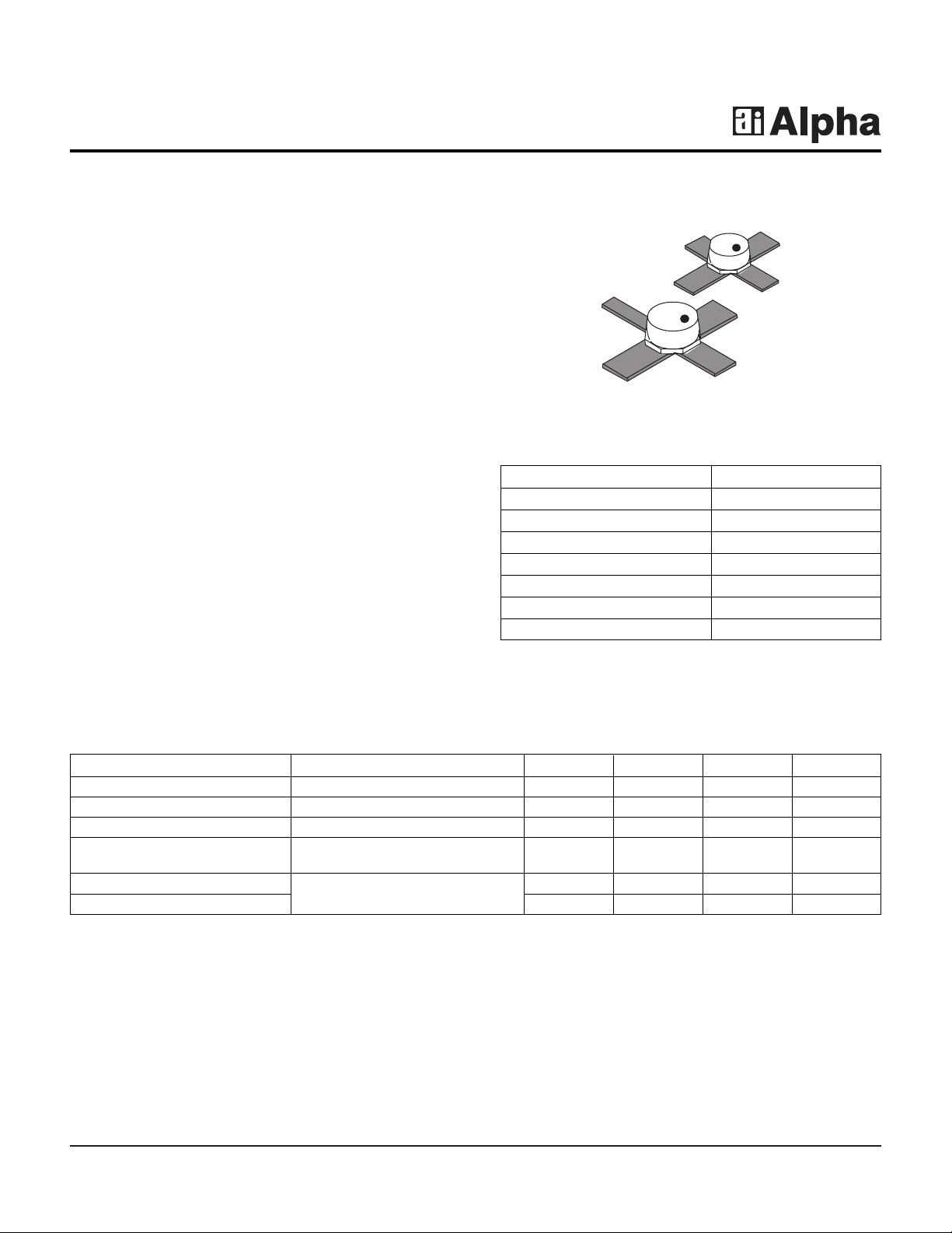
The AFP02N8-212, 213 are general purpose packaged
PHEMT chips that have excellent gain and noise
performance through X band, making them suitable for a
wide range of commercial applications. The devices
employ 0.7 µm Ti/Pd/Au gates and surf ace passiv ation to
ensure a rugged, reliable part. Available in metal cer amic
packages with a choice of two lead lengths. The
components are also available in tape and reel and are
ready for automatic insertion equipment.
AFP02N8-212, AFP02N8-213
Parameter Test Conditions Min. Typ. Max. Unit
Saturated Drain Current (I
DSS
)V
DS
= 2 V, VGS= 0 V 25.0 55.0 90.0 mA
Transconductance (gm) VDS= 2 V, IDS= 15 mA 30.0 45.0 mS
Pinch-off Voltage (VP) VDS= 2 V, IDS= 0.3 mA -0.4 -1.2 -2.0 V
Gate to Source IGS= -200 µA -6.0 8.0 V
Breakdown V oltage (V
bgs
)
Noise Figure (NF)
VDS= 2 V, IDS= 15 mA, F = 4 GHz
1.55 2.0 dB
Associated Gain (GA) 12.0 13.2 dB
Electrical Specifications at 25°C
Source
Gate
Source
Drain
Drain
Source Gate
Source
212
213
Characteristic Value
Drain to Source Voltage (VDS) 6 V
Gate to Source Voltage (VGS) -3 V
Drain Current (IDS) I
DSS
Gate Current (IGS) 10 µA
Total Power Dissipation (PT) 300 mW
Storage Temperature (TST) -65 to +150°C
Channel Temperature (TCH) 175°C
Absolute Maximum Ratings

2 Alpha Industries, Inc. [781] 935-5150 • Fax [617] 824-4579 • Email sales@alphaind.com • www.alphaind.com
Specifications subject to change without notice. 6/99A
General Purpose Packaged PHEMT Chips AFP02N8-212, AFP02N8-213
0
4
8
12
16
20
24
0
024681012141618
1
2
3
4
6
5
NF
MIN
(dB)
G
A
(dB)
Frequency (GHz)
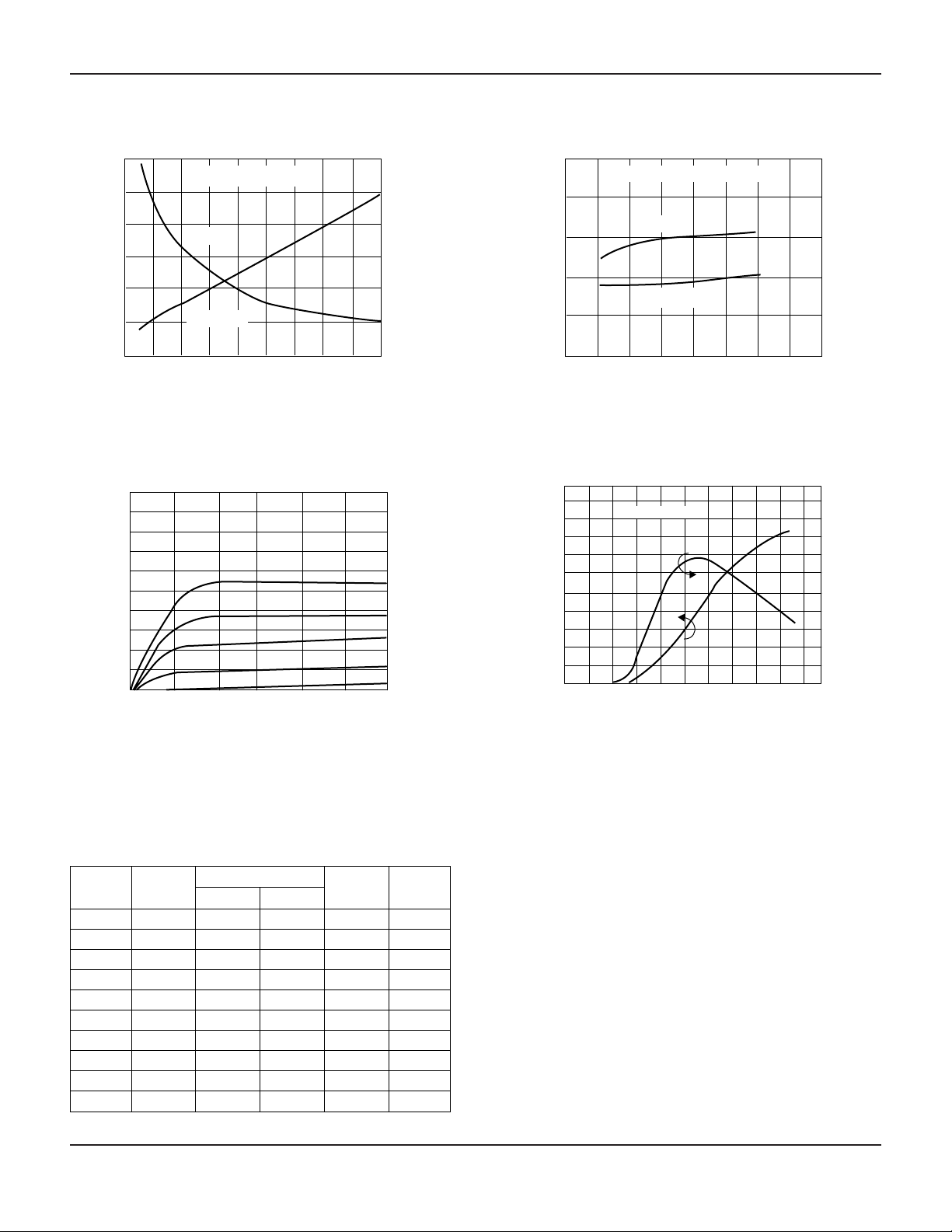
RF Minimum Noise Figure (NF
MIN
) and
Associated Gain (G
A
) vs. Frequency (GHz)
VDS = 2 V, IDS = 15 mA
GA (dB)
NF
MIN
(dB)
100
0 1.0 1.5 2.50.5 2.0 3.0
50
0
VDS (V)
l
DS
(mA)
DC Drain Current (IDS) vs. Drain Voltage (VDS)
as a Function of Gate to Source Voltage (V
GS
)
0 5 10 15 20 25 30 4035
IDS (mA)
NF
MIN
(dB)
G
A
(dB)
RF Minimum Noise Figure (NF
MIN
) and
Associated Gain (G
A
) vs. Drain Current (IDS)
F = 12 GHz, VDS = 2 V
0
2
4
6
8
10
0
2
4
6
10
8
NF
MIN
(dB)
GA (dB)
100
0
-2.0 -1.0 0
100
0
50
50
1.0
gm (mS)
VGS (V)
l
DS
(mA)
VDS = 2 V
DC Drain Current (IDS) and
Transconductance (gm) vs.
Gate to Source Voltage (V
GS
)
Typical Performance Data
Freq. NF
MIN
ΓΓ
opt
(GHz) (dB) Mag. Ang. RN/50 GA(dB)
1 0.75 0.84 25.40 0.12 23.50
2 1.10 0.72 50.20 0.23 18.00
4 1.55 0.54 99.00 0.23 13.20
6 2.00 0.43 145.40 0.15 10.20
8 2.50 0.39 -171.80 0.16 8.10
10 3.00 0.39 -133.60 0.32 6.51
12 3.50 0.43 -100.10 0.66 5.82
14 4.00 0.48 -71.10 1.16 5.20
16 4.50 0.55 -45.90 1.77 4.51
18 5.00 0.60 -23.30 2.38 4.10
Typical Noise Parameters
(V
DS
= 2 V, IDS= 15 mA)
 Loading...