ALPHA AFP02N8-000 Datasheet

Alpha Industries, Inc. [781] 935-5150 • Fax [617] 824-4579 • Email sales@alphaind.com • www.alphaind.com 1
Specifications subject to change without notice. 6/99A
General Purpose PHEMT Chip
Features
■ Low Noise Figure, 1.25 dB @ 4 GHz
■ High Associated Gain, 15.0 dB @ 4 GHz
■ High MAG, > 18 dB @ 4 GHz
■ 0.7 µm Ti/Pd/Au Gates
■ Passivated Surface
Description
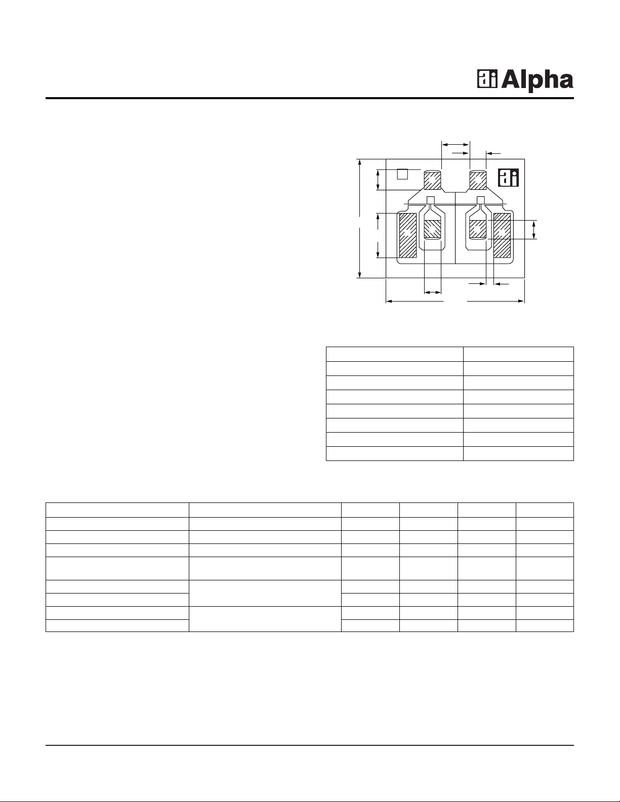
The AFP02N8-000 general purpose PHEMT chip has
excellent gain and noise performance through X band,
making it suitable for a wide range of commercial and military
applications.The device employs 0.7 µm Ti/Pd/Au gates and
surface passivation to ensure a rugged, reliable part.
AFP02N8-000
Parameter Test Conditions Min. Typ. Max. Unit
Saturated Drain Current (I
DSS
)V
DS
= 2 V, VGS= 0 V 25.0 45.0 90.0 mA
Transconductance (gm) VDS= 2 V, IDS= 15 mA 40.0 55.0 mS
Pinch-off Voltage (VP) VDS= 2 V, IDS= 0.3 mA -0.2 -0.6 -2.0 V
Gate to Source IGS= -200 µA -4.0 -6.0 V
Breakdown V oltage (V
bgs
)
Noise Figure (NF)
VDS= 2 V, IDS= 15 mA, F = 4 GHz
1.25 1.75 dB
Associated Gain (GA) 14.0 15.0 dB
Noise Figure (NF)
VDS= 2 V, IDS= 15 mA, F = 12 GHz
2.6 3.0 dB
Associated Gain (GA) 8.5 9.4 dB
Electrical Specifications at 25°C
78
50
50
50
400
50
20
125
350
D
SS
GG
D
Characteristic Value
Drain to Source Voltage (VDS) 6 V
Gate to Source Voltage (VGS) -3 V
Drain Current (IDS) I
DSS
Gate Current (IGS) 10 µA
Total Power Dissipation (PT) 300 mW
Storage Temperature (TST) -65 to +150°C
Channel Temperature (TCH) 175°C
Absolute Maximum Ratings

2 Alpha Industries, Inc. [781] 935-5150 • Fax [617] 824-4579 • Email sales@alphaind.com • www.alphaind.com
Specifications subject to change without notice. 6/99A
General Purpose PHEMT Chip AFP02N8-000
0
4
8
12
16
20
24
0
0 2 4 6 8 10 12 14 16 18 20
1
2
3
4
6
5
NF
MIN
(dB)
G
A
(dB)
Frequency (GHz)
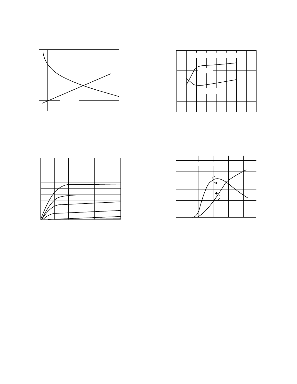
RF Minimum Noise Figure (NF
MIN
) and
Associated Gain (G
A
) vs. Frequency (GHz)
VDS = 2 V, IDS = 15 mA
GA (dB)
NF
MIN
(dB)
100
0 1.0 1.5 2.50.5 2.0 3.0
50
0
VDS (V)
l
DS
(mA)
DC Drain Current (IDS) vs. Drain Voltage (VDS)
as a Function of Gate to Source Voltage (V
GS
)
0 5 10 15 20 25 30 4035
IDS (mA)
NF
MIN
(dB)
G
A
(dB)
RF Minimum Noise Figure (NF
MIN
) and
Associated Gain (G
A
) vs. Drain Current (IDS)
F = 12 GHz, VDS = 2 V
0
2
4
6
8
12
0
1
2
3
4
6
105
NF
MIN
(dB)
GA (dB)
100
0
-2.0 -1.0 0
100
0
50
50
1.0
gm (mS)
VGS (V)
l
DS
(mA)
VDS = 2 V
DC Drain Current (IDS) and
Transconductance (gm) vs.
Gate to Source Voltage (V
GS
)
Typical Performance Data
 Loading...