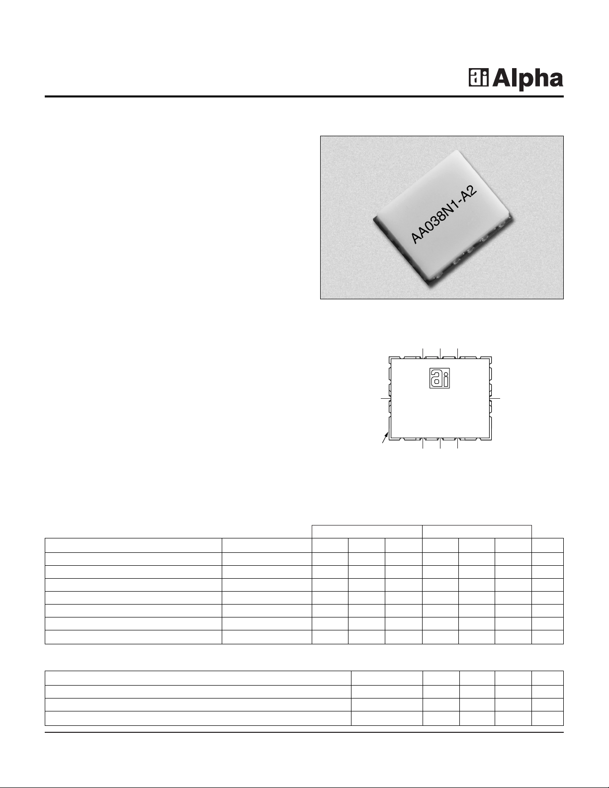
ALPHA AA038N1-A2 Datasheet

Low Band High Band
Alpha Industries, Inc. [781] 935-5150 • Fax [617] 824-4579 • Email sales@alphaind.com • www.alphaind.com 1
Specifications subject to change without notice. 7/00A
26–40 GHz Surface Mount
Low Noise Amplifier
Features
■ Surface Mount Package
■ 3.8 dB Noise Figure
■ 18 dB Gain
■ +5 dBm Output Power
■ Single Voltage Operation
■ 100% RF and DC Testing
AA038N1-A2
Patent Pending
Description
The AA038N1-A2 is a broadband millimeterwave low
noise amplifier in a rugged surface mount package which
is compatible with high-volume solder installation. The
amplifier is designed for use in millimeterwave
communication and sensor systems as the receiver frontend or as a gain stage when high gain and low noise figure
are required. The robust ceramic surface mount package
provides excellent electrical performance and a high
degree of environmental protection for long-term reliability.
A single supply voltage simplifies bias requirements. All
amplifiers are screened at the operating frequencies prior
to shipment for guaranteed performance. Amplifier is
targeted for high-volume millimeterwave applications such
as point-to-point and point-to-multipoint wireless
communications systems.
Parameter Symbol Min. Typ. Max. Min. Typ. Max. Unit
Bandwidth BW 26 36 36 40 GHz
Small Signal Gain G 16 20 14 18 dB
Noise Figure NF 3.5 4.0 3.8 4.2 dB
Input Return Loss RL
I
77dB
Output Return Loss RL
O
10 10 dB
Output Power at 1 dB Gain Compression P
1 dB
4 6 3 5 dBm
Temperature Coefficient of Gain dG/dT -0.024 -0.024 dB/C
Electrical Specifications at 25°C (VD1= VD2= 5.5 V)
Parameter Symbol Min. Typ. Max. Unit
Drain Current 1 I
D1
27 mA
Drain Current 2 I
D2
1mA
Total Drain Current ID1+ I
D2
28 36.5 mA
DC
RF
Pin Out
AA038N1-A2
YYWW
RF In RF Out
Orientation
Indicated by
Missing
Castellations
V
D1
N/CN/C
V
D2
N/CN/C

26–40 GHz Surface Mount Low Noise Amplifier AA038N1-A2
2 Alpha Industries, Inc. [781] 935-5150 • Fax [617] 824-4579 • Email sales@alphaind.com • www.alphaind.com
Specifications subject to change without notice. 7/00A
Characteristic Value
Operating Temperature (TC) -55°C to +90°C
Storage Temperature (TST) -65°C to +150°C
Bias Voltage (VD1)6 V
DC
Bias Voltage (VD2)6 V
DC
Power In (PIN) 13 dBm
Absolute Maximum Ratings
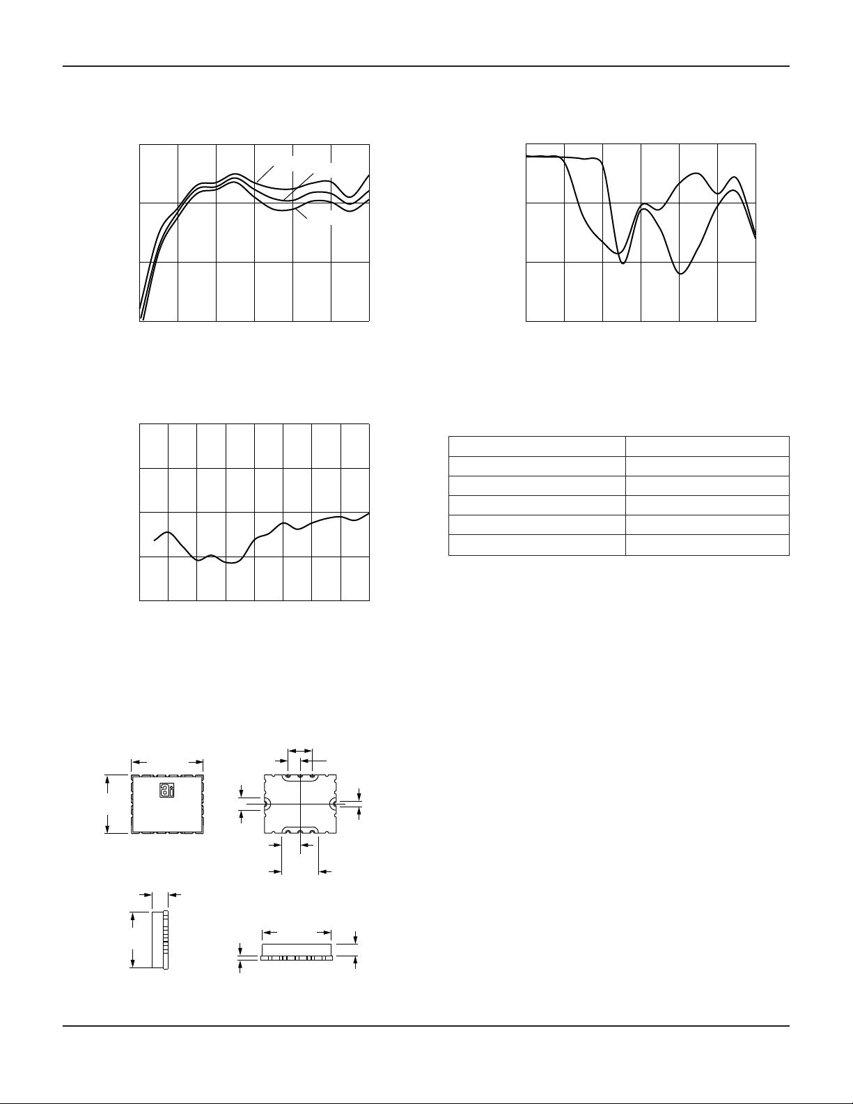
Frequency (GHz)
Gain vs. Frequency
Gain (dB)
0
10
20
30
16 20 24 28 32 36 40
-55˚C
+85˚C
+25˚C
Frequency (GHz)
Noise Figure vs. Frequency
NF (dB)
2
3
4
5
6
24 26 28 30 32 34 36 38 40
Frequency (GHz)
Return Loss vs. Frequency
Return Loss (dB)
S
11
S
22
-30
-20
-10
0
16 20 24 28 32 36 40
Typical Performance Data (VD1= VD2= 5.5 V)
Outline
0.241
(6.12 mm)
0.040
(1.02 mm)
0.016
(0.41 mm)
0.194
(4.93 mm)
0.056
(1.42 mm)
0.204
(5.18 mm)
0.251
(6.38 mm)
2X 0.044
(1.12 mm)
8X 0.020
(0.51 mm)
2X 0.129
(3.28 mm)
C
L
2X 0.064
(1.63 mm)
2X 0.043
(1.09 mm)
2X 0.085
(2.16 mm)
C
L
 Loading...