ALPHA AA038N1-99 Datasheet

Alpha Industries, Inc. [781] 935-5150 • Fax [617] 824-4579 • Email sales@alphaind.com • www.alphaind.com 1
Specifications subject to change without notice. 10/99A
26–41 GHz Low Noise Amplifier
Features
■ 3.8 dB Noise Figure
■ 18 dB Gain
■ +5 dBm Output Power
■ Rugged, Reliable Package
■ Single Voltage Operation
■ 100% RF and DC Testing
Block Diagram
AA038N1-99
Description
The AA038N1-99 is a broadband millimeterwave amplifier
in a rugged package.The amplifier is designed for use in
millimeterwave communication and sensor systems as the
receiver front-end or transmitter gain stage when high
gain, wide dynamic range, and low noise figure are
required. The robust ceramic and metal package provides
excellent electrical performance, excellent thermal
performance, and a high degree of environmental
protection for long-term reliability. A single supply voltage
simplifies bias requirements. All amplifiers are screened
at the operating frequencies prior to shipment for
guaranteed performance. Amplifier is targeted for
millimeterwave point-to-point and point-to-multipoint
wireless communications systems.
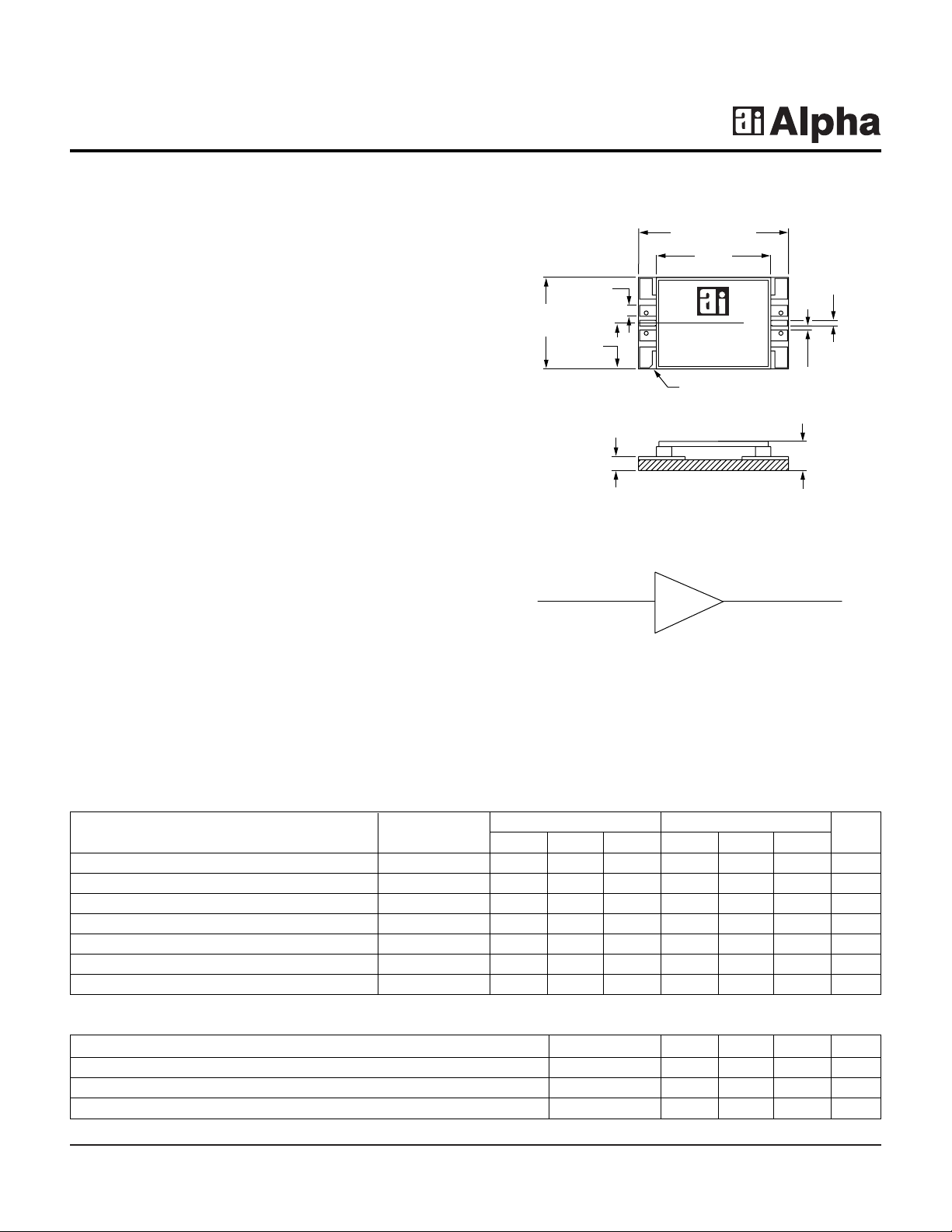
0.057
(1.45 mm)
0.011
(0.28 mm)
0.022
(0.56 mm)
0.090
(2.29 mm)
0.028
(0.71 mm)
0.180
(4.57 mm)
0.225
(5.72 mm)
0.295 (7.49 mm)
0.008
(0.20 mm)
PIN 1
INDICATOR
AA038N1-99
YYWW
LNA
Parameter Symbol Min. Typ. Max. Unit
Drain Current 1 I
D1
27 mA
Drain Current 2 I
D2
1mA
Total Drain Current ID1+ I
D2
28 36.5 mA
DC
Low Band High Band
Parameter Symbol Min. Typ. Max. Min. Typ. Max. Unit
Bandwidth BW 26 24–36 36 36 36–42 41 GHz
Small Signal Gain G 16 22 14 18 dB
Noise Figure NF 3.8 4.5 3.8 4.2 dB
Input Return Loss RL
I
11 9 dB
Output Return Loss RL
O
15 10 dB
Output Power at 1 dB Gain Compression P
1 dB
4 6 3 5 dBm
Temperature Coefficient of Gain dG/dT -0.024 -0.024 dB/C
RF
Electrical Specifications at 25°C (VD1= VD2= +5.5 V)

26–41 GHz Low Noise Amplifier AA038N1-99
2 Alpha Industries, Inc. [781] 935-5150 • Fax [617] 824-4579 • Email sales@alphaind.com • www.alphaind.com
Specifications subject to change without notice. 10/99A
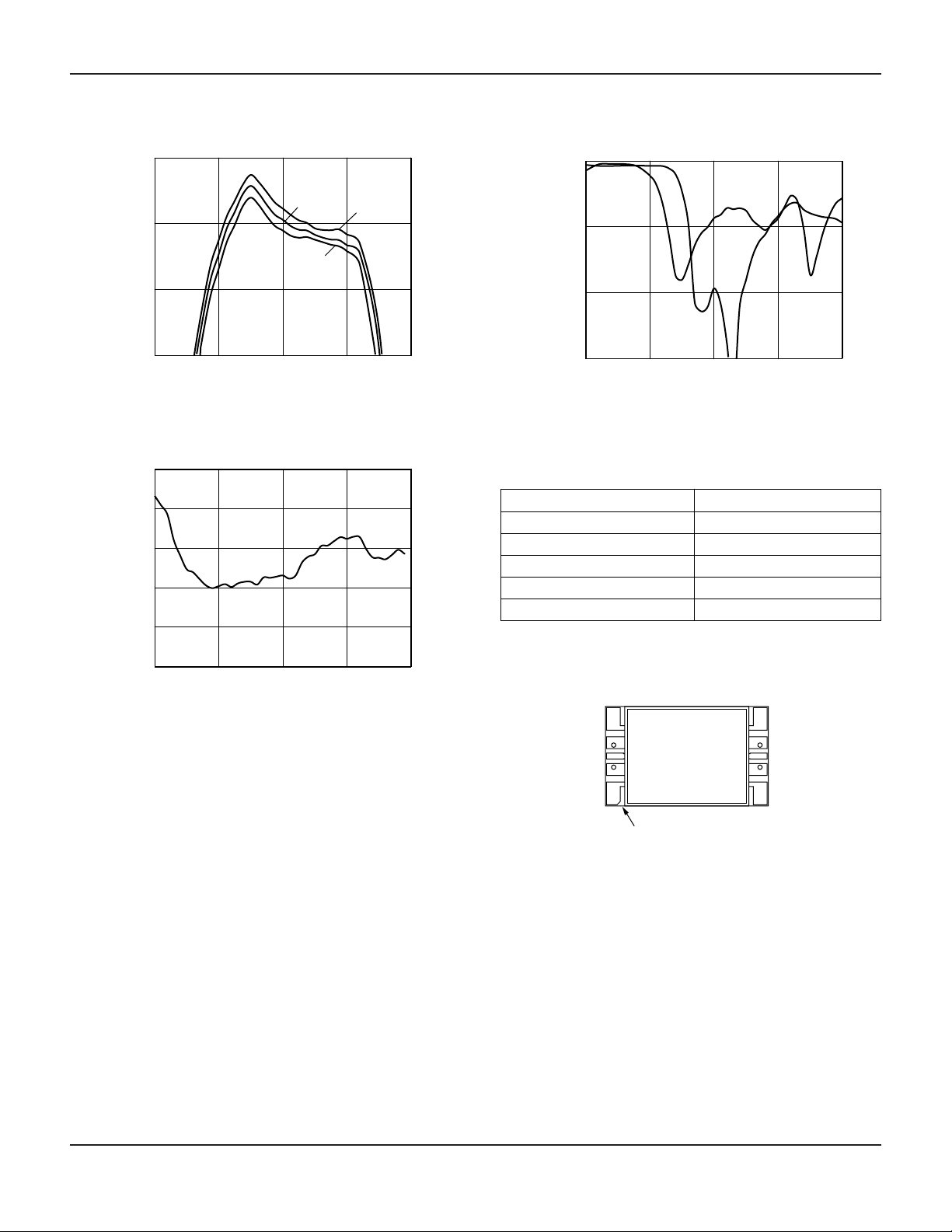
Frequency (GHz)
Gain vs. Frequency
Gain (dB)
0
10
20
30
10 20 30 40 50
-55˚C
90˚C
25˚C
Frequency (GHz)
Noise Figure vs. Frequency
2
1
3
4
5
6
20 25 30 35 40
NF (dB)
Frequency (GHz)
Return Loss vs. Frequency
-30
-20
-10
0
Return Loss (dB)
S
22
S
11
10 20 30 40 50
Typical Performance Data
Pin Out
RF In
PIN 1
INDICATOR
V
D2
N/C
V
D1
N/C
RF Out
Characteristic Value
Operating Temperature (TOP) -55°C to +90°C
Storage Temperature (TST) -65°C to +150°C
Bias Voltage (VD1)6 V
DC
Bias Voltage (VD2)6 V
DC
Power In (PIN) 13 dBm
Absolute Maximum Ratings
 Loading...