

Page 1

Parameter
Symbol
Minimum
Maximum
Units
Storage Temperature
Tst
-40
+85
C
Supply Voltage
Vcc 0 +3.6
V
Operating Relative Humidity
RH 0 85
%
Parameter
Symbol
Min
Typical
Max
Units
Supply Voltage
Vcc
3.15
3.45
V
ALLNET ALL4757
ALLNET ALL4757 Modul
Product Specification
10Gbps SFP+ Transceiver, 850nm MM 300m DDM
Feature:
SFP+ package with LC connector
850nm VCSEL Laser and PIN photo detector
Up to 300m transmission on 2000MHz-km MMF
Power dissipation < 1W
LVPECL compatible data input/output interface
Low EMI and excellent ESD protection
laser safety standard IEC-60825 compliant
Compatible with RoHS
Compatible with SFF8472
Application
Ethernet
Fiber Channel
Absolute Maximum Ratings
Operation Environment
ALLNET GmbH Computersysteme, Maistr.2, 82110 Germering
Page 2

Operating Case
Temperature
Commercial
Tc 0
+70
C
Power Dissipation
1 W
Data Rate
10.3125
Gbps
Parameter
Symbol
Min.
Typ.
Max.
Units
Transmitter Section
Center Wavelength
o
840
850
860
nm
RMS Spectral Width
- - 0.45
dB
Average Output Power
Po
-5 - -1
dBm
Extinction Ratio
Er
3.0 - -
dB
Dispersion Penalty
3.9
dB
Relative Intensity Noise
RIN12OMA
-128
dB/Hz
Total jitter
Tj
IEEE 802.3ae
Receiver Section
Center Wavelength
o
850 nm
Receiver Sensitivity
Rsen
-11.5
dBm
Stressed Sensitivity
Rsen
7.5
dBm
Receiver Overload
Rov
0
dBm
Return Loss
12
dB
LOS Assert
LOSA
-17
dBm
LOS Dessert
LOSD
-15
dBm
LOS Hysteresis
0.5 4
ALLNET ALL4757
ALLNET ALL4757 Modul
Optical Characteristics
(Ambient Operating Temperature 0C to +70C, Vcc =3.3 V)
ALLNET GmbH Computersysteme, Maistr.2, 82110 Germering
Page 3

Parameter
Symbol
Min.
Typ.
Max.
unit
Transmitter Section
Input Differential Impendence
Zin
90
100
110
Ohm
Data Input Swing Differential
Vin
180
700
mV
TX Disable
Disable
2.0 Vcc
V
Enable 0 0.8
V
TX Fault
Assert
2.0 Vcc
V
Deassert
0
0.8
V
Receiver Section
Output differential impendence
Zout
100
Ohm
Data output Swing Differential
Vout
300
800
mV
Rx_LOS
Assert
2.0 Vcc
V
Deassert
0
0.8
V
Parameter
Symbol
Min.
Typ.
Max.
unit
Input Differential Impendence
Zin
90
100
110
Ohm
Data Input Swing Differential
Vin
180
700
mV
Fiber Type
850nm OFL
BandWidth
62.5 um
160MHz-km
26
m
200MHz-km
33
m
50 um
400MHz-km
66
m
500MHz-km
82
m
2000MHz-km
300
m
ALLNET ALL4757
ALLNET ALL4757 Modul
Electrical Characteristics
(Ambient Operating Temperature 0C to +70C, Vcc =3.3 V)
Maximum Supported Distances
ALLNET GmbH Computersysteme, Maistr.2, 82110 Germering
Page 4
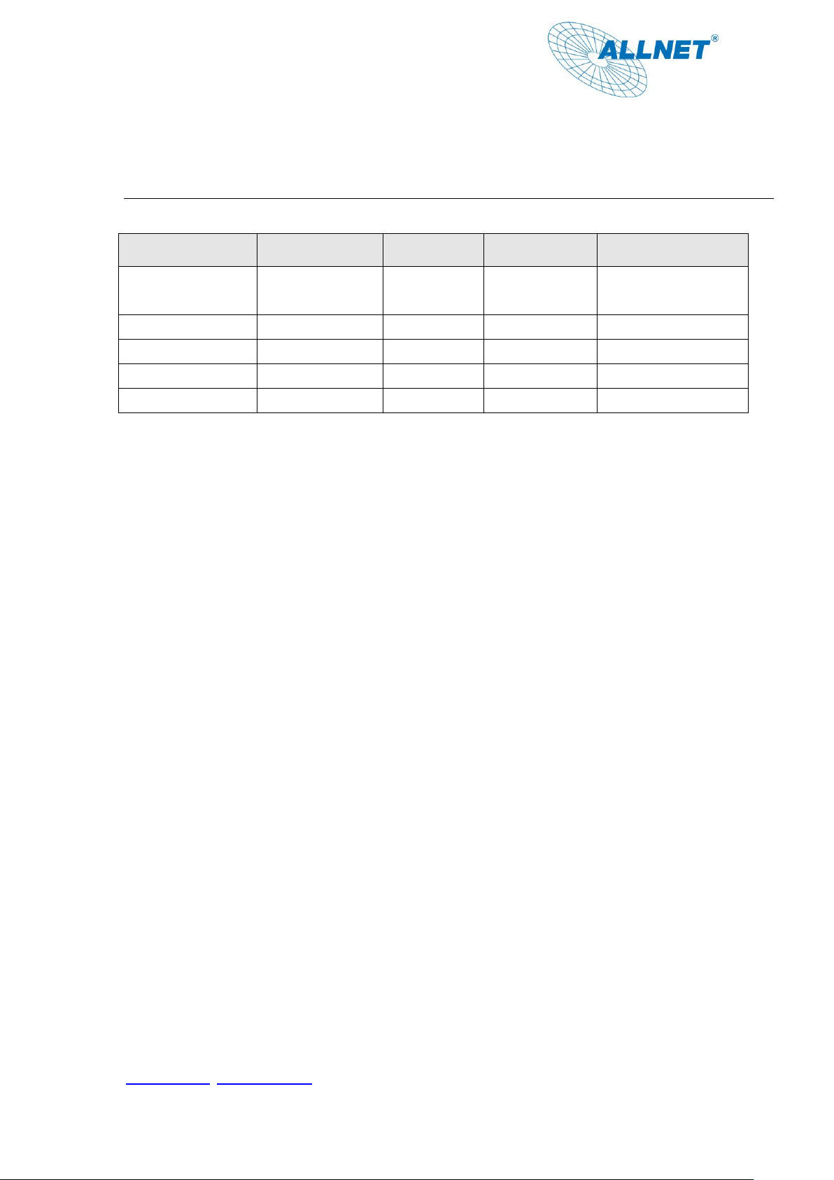
Parameter
Range
Accuracy
Unit
Calibration
Temperature
-5 ~ 75
±3
ºC
Internal
Voltage
0 ~ VCC
0.1
V
Internal
Bias Current
0 ~ 120
0.5
mA
Internal
Tx Power
0 ~ 5
±1
dB
Internal
Rx Power
-25 ~ -3
±1
dB
Internal
ALLNET ALL4757
ALLNET ALL4757 Modul
Diagnostics
ALLNET GmbH Computersysteme, Maistr.2, 82110 Germering
Page 5
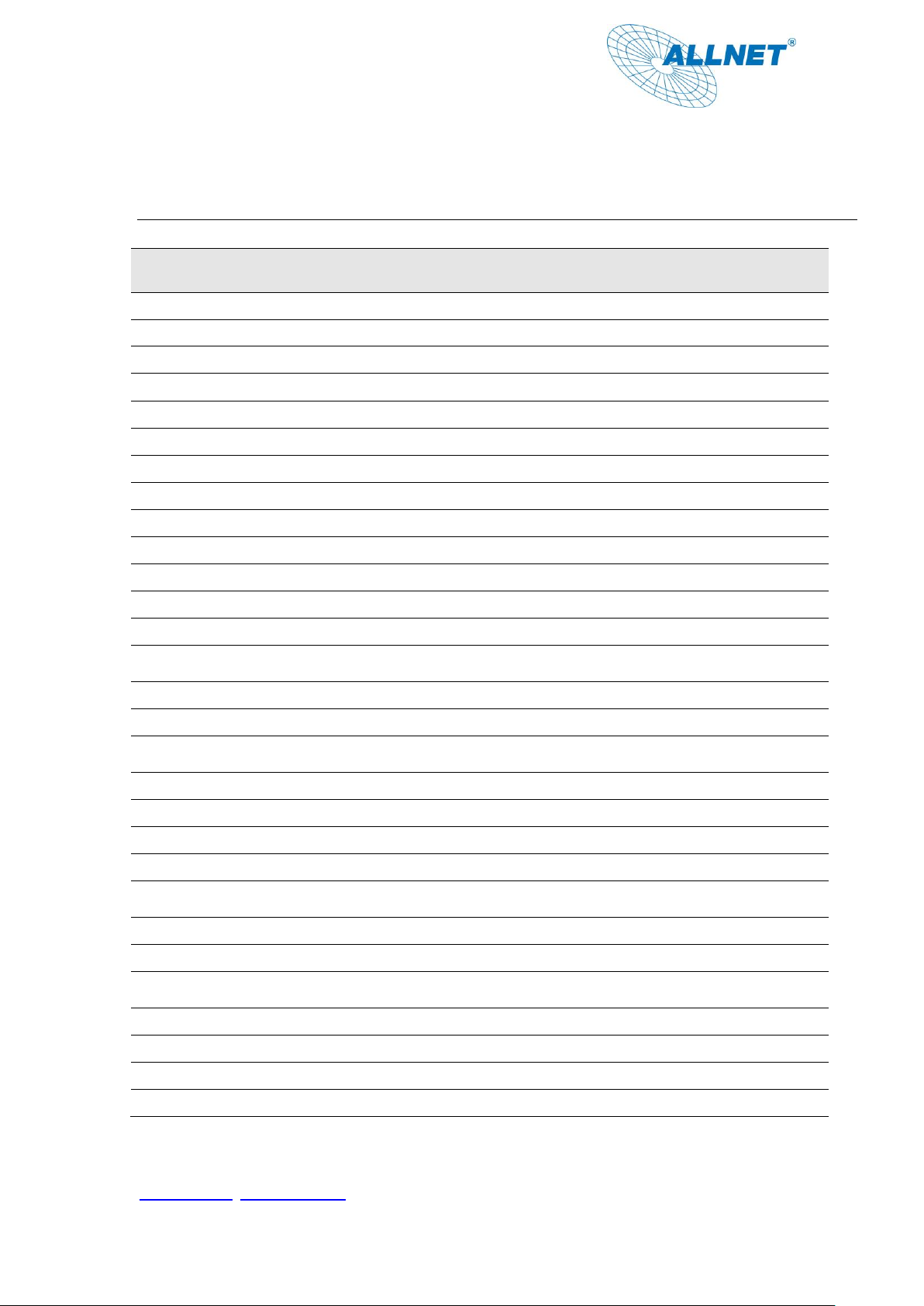
Addr
Field Size
(Bytes)
Name of Field
HEX
Description
0
1
Identifier
03
SFP
1
1
Ext. Identifier
04
MOD4
2
1
Connector
07
LC
3-10
8
Transceiver
10 00 00 00 00 00 00 00
Transmitter Code
11
1
Encoding
06
64B66B
12
1
BR, nominal
67
1000M bps
13
1
Reserved
00
14
1
Length (9um)-km
00
15
1
Length (9um)
00
16
1
Length (50um)
08
17
1
Length (62.5um)
02
18
1
Length (copper)
00
19
1
Reserved
00
20-35
16
Vendor name
57 49 4E 54 4F 50 20 20
20 20 20 20 20 20 20 20
WINTOP
36
1
Reserved
00
37-39
3
Vendor OUI
00 00 00
40-55
16
Vendor PN
xx xx xx xx xx xx xx xx
xx xx xx xx xx xx xx xx
ASC II
56-59
4
Vendor rev
31 2E 30 20
V1.0
60-61
2
Wavelength
03 52
850nm
62
1
Reserved
00
63
1
CC BASE
XX
Check sum of byte 0~62
64-65
2
Options
00 1A
LOS, TX_DISABLE,
TX_FAULT
66
1
BR, max
00
67
1
BR, min
00
68-83
16
Vendor SN
00 00 00 00 00 00 00 00
00 00 00 00 00 00 00 00
Unspecified
84-91
8
Vendor date code
XX XX XX 20
Year, Month, Day
92-94
3
Reserved
00
95
1
CC_EXT
XX
Check sum of byte 64~94
96-255
160
Vendor specific
ALLNET ALL4757
ALLNET ALL4757 Modul
EEPROM INFORMATION(A0):
ALLNET GmbH Computersysteme, Maistr.2, 82110 Germering
Page 6
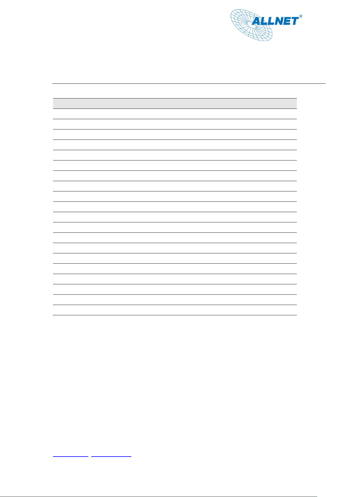
Pins
Name
Discription
NOTE
1
VeeT
Transmitter Ground
2
Tx Fault
Transmitter Fault Indication
1
3
Tx Disable
Transmitter Disable
2
4
MOD DEF2
Module Definition 2
3
5
MOD DEF1
Module Definition 1
3
6
MOD DEF0
Module Definition 0
3
7
RS0
Not Connected
8
LOS
Loss of Signal
4
9
RS1
Not Connected
10
VeeR
Receiver Ground
11
VeeR
Receiver Ground
12
RD-
Inv. Received Data Output
5
13
RD+
IReceived Data Output
5
14
VeeR
Receiver Ground
15
VccR
Receiver Power
16
VccT
Transmitter Power
17
VeeT
Transmitter Ground
18
TD+
Transmit Data Input
6
19
TD-
Inv. Transmit Data Input
6
20
VeeT
Transmitter Ground
ALLNET ALL4757
ALLNET ALL4757 Modul
Pin Description:
Notes:
1. TX Fault is an open collector output, which should be pulled up with a 4.7k~10kΩ resistor on the
host board to a voltage between 2.0V and Vcc+0.3V. Logic 0 indicates normal operation; logic 1
indicates a laser fault of some kind. In the low state, the output will be pulled to less than 0.8V.
2. TX Disable is an input that is used to shut down the transmitter optical output. It is pulled up within
the module with a 4.7k~10kΩ resistor. Its states are:
Low (0~0.8V): Transmitter on
(>0.8V, <2.0V): Undefined
High (2.0~3.465V): Transmitter Disabled
Open: Transmitter Disabled
3. MOD-DEF 0,1,2 are the module definition pins. They should be pulled up with a 4.7k~10kΩ
resistor on
the host board. The pull-up voltage shall be VccT or VccR.
MOD-DEF 0 is grounded by the module to indicate that the module is present
MOD-DEF 1 is the clock line of two wire serial interface for serial ID
ALLNET GmbH Computersysteme, Maistr.2, 82110 Germering
Page 7
ALLNET ALL4757
ALLNET ALL4757 Modul
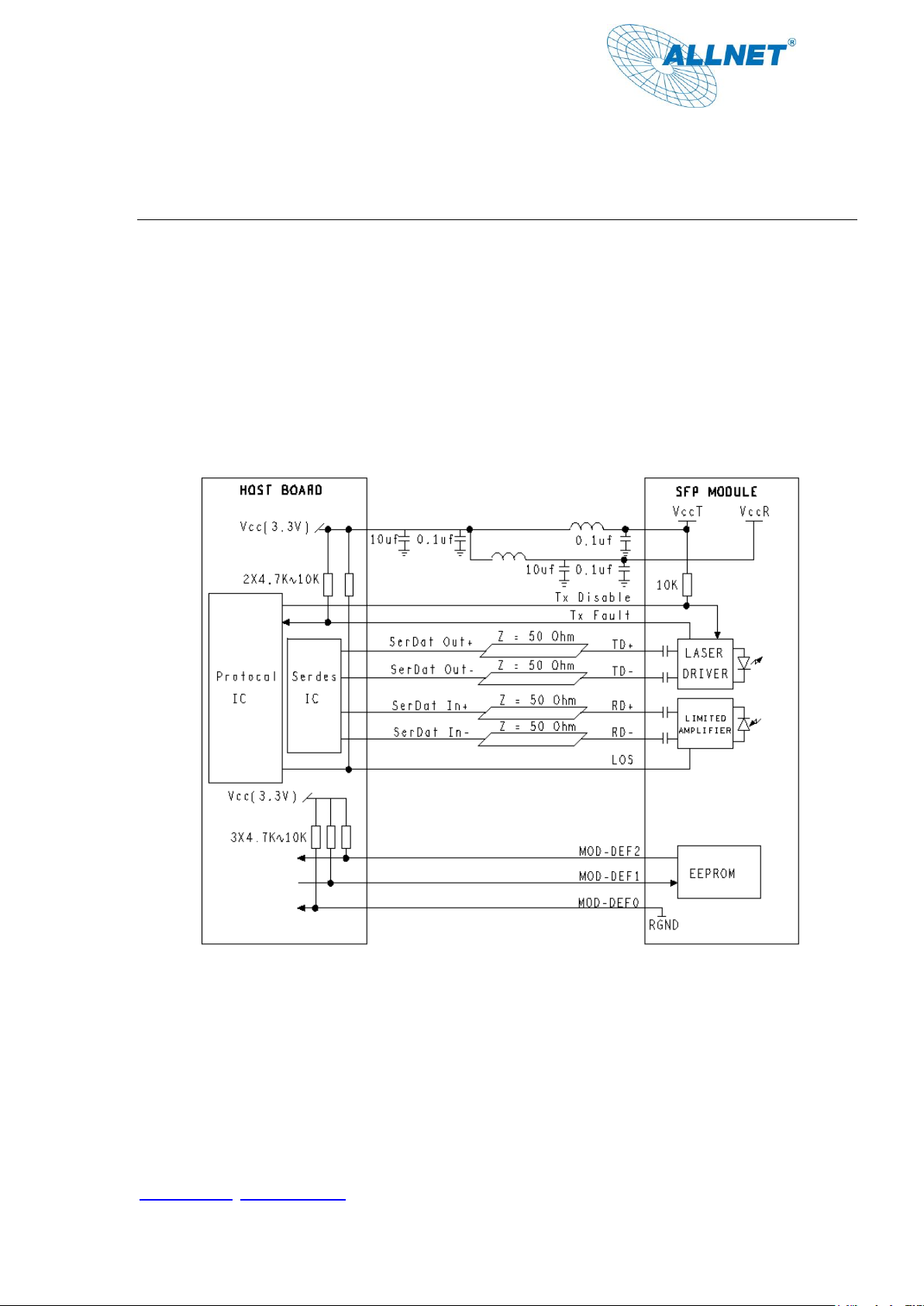
MOD-DEF 2 is the data line of two wire serial interface for serial ID
4. LOS is an open collector output, which should be pulled up with a 4.7k~10kΩ resistor on the host
board to a voltage between 2.0V and Vcc+0.3V. Logic 0 indicates normal operation; logic 1 indicates
loss of signal. In the low state, the output will be pulled to less than 0.8V.
5. These are the differential receiver output. They are internally AC-coupled 100Ω differential lines
which should be terminated with 100Ω (differential) at the user SERDES.
6. These are the differential transmitter inputs. They are AC-coupled, differential lines with 100Ω
differential termination inside the module.
Recommended Application Circuit
ALLNET GmbH Computersysteme, Maistr.2, 82110 Germering
Page 8
ALLNET ALL4757
ALLNET ALL4757 Modul
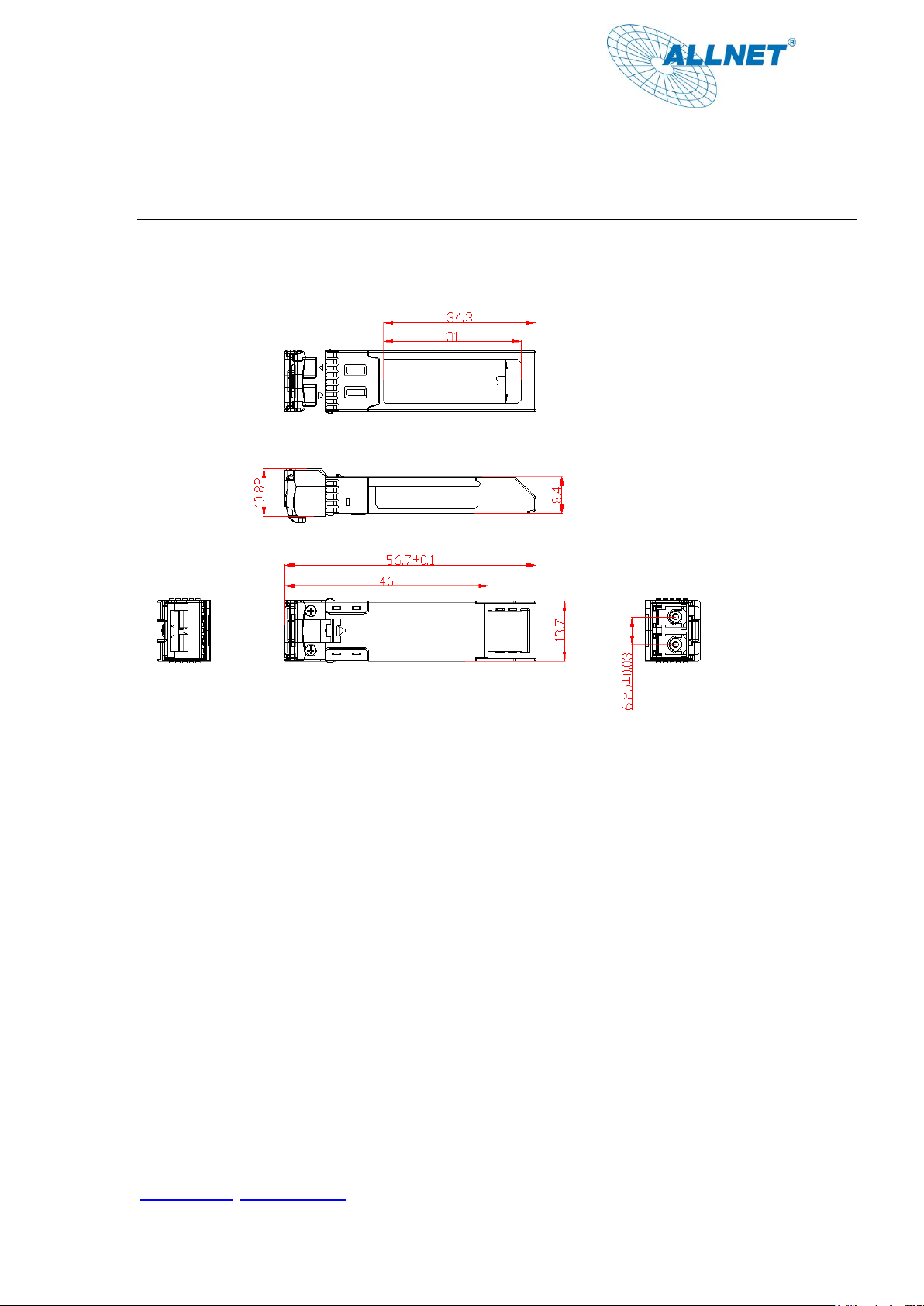
Outline drawing (mm):
ALLNET GmbH Computersysteme, Maistr.2, 82110 Germering
 Loading...