

Alliance Semiconductor Corporation AS4C256K16F0-30TI, AS4C256K16F0-30TC, AS4C256K16F0-30JI, AS4C256K16F0-30JC, AS4C256K16F0-25TI Datasheet
...
5V 256K X 16 CMOS DRAM (Fast Page Mode)
Features
• Organization: 262,144 words × 16 bits
• High speed
- 25/30/35/50 ns RAS
- 12/16/18/25 ns column address access time
- 7/10/10/10 ns CAS
• Low power consumption
- Active: 770 mW max (ASAS4C256K16FO-50)
- Standby: 5.5 mW max, CMOS I/O
•Fast page mode
• AS4C256K16FO-50 timings
AS4C256K16FO-60.
access time
access time
are also valid for
AS4C256K16FO
®
•Refresh
- 512 refresh cycles, 8 ms refresh interval
-RAS
-only or CAS-before-RAS refresh or self-refresh
- Self-refresh option is available for new generation
device only. Contact Alliance for more information.
• Read-modify-write
• TTL-compatible, three-state I/O
• JEDEC standard packages
- 400 mil, 40-pin SOJ
- 400 mil, 40/44-pin TSOP II
• Single 5V power supply/built-in V
• Latch-up current > 200 mA
generator
bb
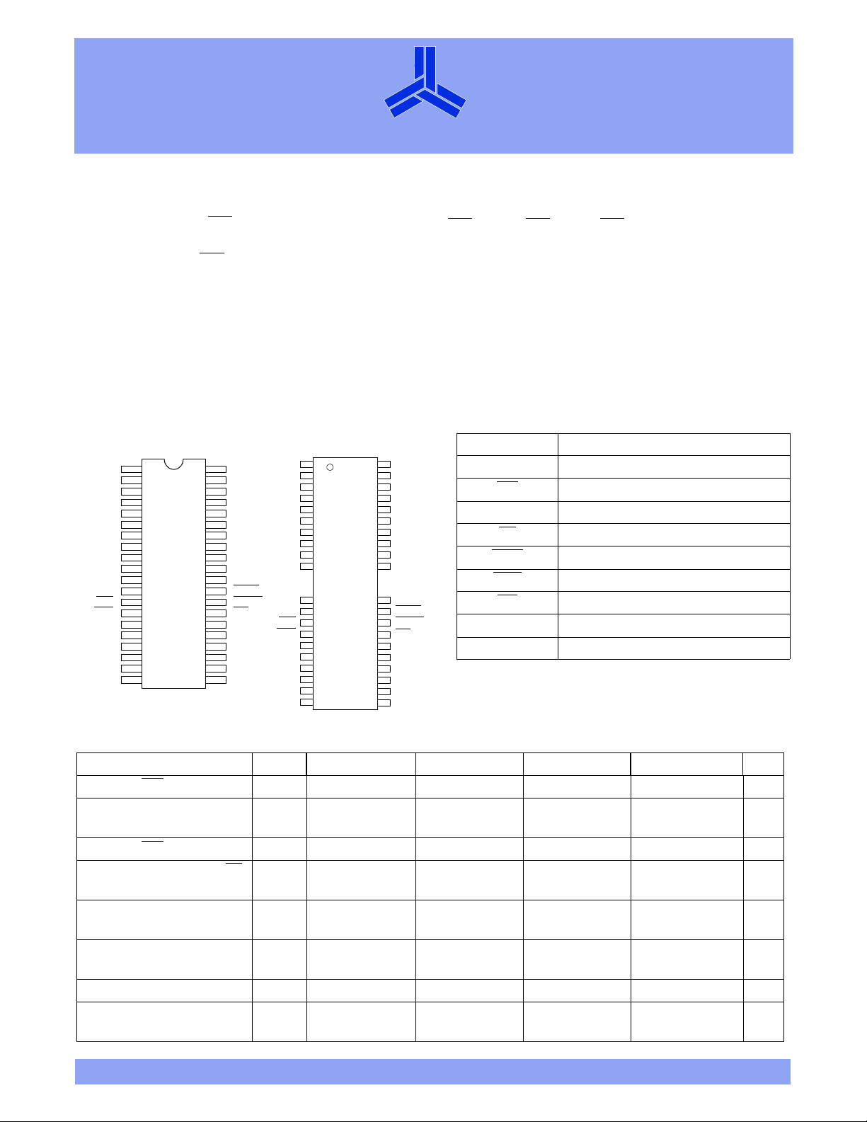
Pin arrangement
SOJ
40
V
I/O0
I/O1
I/O2
I/O3
V
I/O4
I/O5
I/O6
I/O7
NC
NC
WE
RAS
NC
A0
A1
A2
A3
V
10
11
12
13
14
15
16
17
18
19
20
1
2
3
4
5
6
7
8
9
ASC256K16FO
CC
CC
CC
39
38
37
36
35
34
33
32
31
30
29
28
27
26
25
24
23
22
21
GND
I/O15
I/O14
I/O13
I/O12
GND
I/O11
I/O10
I/O9
I/O8
NC
LCAS
UCAS
OE
A8
A7
A6
A5
A4
GND
Selection guide
Maximum RAS
Maximum column address
access time
Maximum CAS
Maximum output enable (OE
access time
Minimum read or write cycle
time
Minimum EDO page mode
cycle time
Maximum operating current I
Maximum CMOS standby
current
access time t
access time t
)
Pin designation
TSOP II
V
I/O0
I/O1
I/O2
I/O3
V
I/O4
I/O5
I/O6
I/O7
NC
NC
WE
RAS
NC
A0
A1
A2
A3
V
CC
CC
CC
1
2
3
4
5
6
7
8
9
10
13
14
15
16
17
18
19
20
21
22
ASC256K16FO
44
43
42
41
40
39
38
37
36
35
32
31
30
29
28
27
26
25
24
23
V
SS
I/O15
I/O14
I/O13
I/O12
V
SS
I/O11
I/O10
I/O9
I/O8
NC
LCAS
UCAS
OE
A8
A7
A6
A5
A4
V
SS
Symbol –25 –30 –35 –50 Unit
RAC
t
CAA
CAC
t
OEA
t
t
CC1
I
CC2
RC
PC
25 30 35 50 ns
12 16 18 25 ns
7101010ns
7101010ns
40 65 70 85 ns
12 12 14 25 ns
200 180 160 140 mA
2.0 2.0 2.0 2.0 mA
Pin(s) Description
A0 to A8 Address inputs
RAS
Row address strobe
I/O0 to I/O15 Input/output
OE
Output enable
UCAS Column address strobe, upper byte
LCAS
WE
V
CC
Column address strobe, lower byte
Read/write control
Power (+5V ± 10%)
GND Ground
4/11/01; V.0.9.1 Alliance Semiconductor P. 1 of 25
Copyright © Alliance Semiconductor. All rights reserved.
AS4C256K16FO
®
Functional description
The AS4C256K16FO is a high-performance 4 megabit CMOS Dynamic Random Access Memory (DRAM) device organized as
262,144 words × 16 bits. The AS4C256K16FO is fabricated with advanced CMOS technology and designed with innovative
design techniques resulting in high speed, extremely low power and wide operating margins at component and system levels.
The AS4C256K16FO features a high-speed page mode operation in which high speed read, write and read-write are performed
on any of the 512 × 16 bits defined by the column address. The asynchronous column address uses an extremely short row
address capture time to ease the system-level timing constraints associated with multiplexed addressing. Output is tri-stated by a
column address strobe (CAS
system design.
Refresh on the 512 address combinations of A0–A8 during an 8 ms period is accomplished by performing any of the following:
•RAS-only refresh cycles
• Hidden refresh cycles
•CAS-before-RAS refresh cycles
• Normal read or write cycles
• Self-refresh cycles.
*
The AS4C256K16FO is available in standard 40-pin plastic SOJ and 44-pin TSOP II packages compatible with widely available
automated testing and insertion equipment. System level features include single power supply of 5V ± 10% tolerance and direct
interface with TTL logic families.
) which acts as an output enable independent of RAS. Very fast CAS to output access time eases
Logic block diagram
V
CC
GND
A0
A1
RAS
UCAS
LCAS
WE
RAS clock
generator
clock
CAS
generator
WE clock
generator
A2
A3
A4
A5
A6
A7
A8
Recommended operating conditions
Parameter Symbol Min Typ Max Unit
Supply voltage
Input voltage
Column decoder
Refresh
controller
Addreess buffers
Row decoder
V
CC
Sense amp
512×512×16
array
(4,194,304)
4.5 5.0 5.5 V
Data
I/O
buffer
bias generator
I/O0 to I/O15
OE
Substrate
GND 0.0 0.0 0.0 V
V
IH
V
IL
2.4 – VCC + 1 V
–1.0 – 0.8 V
* Self-refresh option is available for new generation device only. Contact Alliance for more information.
4/11/01; V.0.9.1 Alliance Semiconductor P. 2 of 25
AS4C256K16FO
®
Absolute maximum ratings
Parameter Symbol Min Max Unit
Input voltage V
Output voltage V
Power supply voltage V
Operating temperature T
Storage temperature (plastic) T
Soldering temperature × time T
Power dissipation P
Short circuit output current I
IN
OUT
CC
OPR
STG
SOLDER
D
OUT
Latch-up current 200 – mA
Note: Stresses greater than those listed under Absolute Maximum Ratings may cause permanent damage to the device. This is a stress rating only and functional
operation of the device at these or any other conditions outside those indicated in the operational sections of this specification is not implied. Exposure to
absolute maximum rating conditions for extended periods may affect reliability.
–1.0 +7.0 V
–1.0 +7.0 V
–1.0 +7.0 V
0+70°C
–55 +150 °C
–260 × 10 °C × sec
–1W
–50mA
DC electrical characteristics (VCC = 5 ± 10%, GND = 0V, T
–25–30–35–50
Parameter Symbol Test conditions
Input leakage
current
Output leakage
current
Operating
power supply
current
TTL standby
power supply
current
Ave r age powe r
supply current,
RAS
refresh
mode
Fast page mode
average power
supply current
CMOS standby
power supply
current
-before-RAS
CAS
refresh power
supply current
Output voltage
Self refresh
current
I
I
I
I
I
I
I
V
V
I
I
IL
OL
CC1
CC2
CC3
CC4
CC5
CC6
OH
OL
CC7
0V ≤ VIN ≤ + 5.5V
pins not under test = 0V
D
disabled,
OUT
0V ≤ V
OUT
≤ + 5.5V
RAS, UCAS, LCAS, address
cycling; t
= min
RC
–1010–1010–1010–1010µA
–1010–1010–1010–1010µA
–200–180–160–140mA1,2
RAS = UCAS = LCAS = VIH – 2.0 – 2.0 – 2.0 – 2.0 mA
RAS cycling,
UCAS
= LCAS = VIH,
t
= min
RC
RAS = UCAS = LCAS = VIL,
address cycling: t
= min
SC
RAS = UCAS = LCAS =
V
– 0.2V
CC
RAS, UCAS, LCAS, cycling;
t
= min
RC
I
= – 5.0 mA 2.4 – 2.4 – 2.4 – 2.4 – V
OUT
I
= 4.2 mA – 0.4 – 0.4 – 0.4 – 0.4 V
OUT
–120–200–190–140mA1
–130–190–180– 70mA1,2
– 0.60 – 1.0 – 1.0 – 1.0 mA
–120–200–190–140mA1
RAS = UCAS = LCAS = VIL, WE
= OE
= A0 – A8 = VCC –0.2V,
DQ0 – DQ15 = V
– 0.2V, 0.2V
CC
– 2.0 – 2.0 – 2.0 – 2.0 mA
are open
= 0° C to +70° C)
a
Unit NoteMin Max Min Max Min Max Min Max
4/11/01; V.0.9.1 Alliance Semiconductor P. 3 of 25

AS4C256K16FO
®
AC parameters common to all waveforms (VCC = 5V ± 10%, GND = 0V, T
Standard
Symbol Parameter
t
t
t
t
t
RAD
t
RSH(R)
t
t
t
t
RAH
t
t
Random read or write cycle time 45 – 65 – 70 – 85 – ns
RC
RAS precharge time 15 – 25 – 25 – 25 – ns
t
RP
RAS pulse width 25 75K 30 75K 35 75K 50 75K ns
RAS
CAS pulse width 4 – 5 – 6 – 10 – ns
CAS
RAS to CAS delay time 10 17 15 20 16 24 15 35 ns 6
RCD
RAS to column address delay time8 13101411171525 ns 7
CAS to RAS hold time (read cycle) 7 – 10 – 10 – 10 – ns
RAS to CAS hold time 20 – 30 – 35 – 50 – ns
CSH
CAS to RAS precharge time 5–5–5–5–ns
CRP
Row address setup time 0–0–0–0–ns
ASR
Row address hold time 5–5–6–9–ns
t
Transition time (rise and fall) 1.5 50 1.5 50 1.5 50 3 50 ns 4,5
T
Refresh period –8–8–8–8ms3
REF
CAS to output in low Z 0–0–0–3–ns8
CLZ
–25 –30 –35 –50
Read cycle (VCC = 5V±10%, GND = 0V, T
Standard
Symbol Parameter
t
t
t
t
AR(R)
t
t
RCH
t
RRH
t
t
CPN
t
Access time from RAS – 25 – 30 – 35 – 50 ns 6
RAC
Access time from CAS –7 – 10 – 10–10ns6,13
CAC
Access time from address – 12 – 16 – 18 – 25 ns 7,13
AA
Column add hold from RAS 19 – 26 – 28 – 30 – ns
Read command setup time 0 – 0 – 0 – 0 – ns
RCS
Read command hold time to CAS 0–0–0–0–ns9
Read command hold time to RAS 0–0–0–0–ns9
Column address to RAS Lead time 12 – 16 – 18 – 25 – ns
RAL
CAS precharge time 4–3–4 – 5–ns
Output buffer turn-off time 0 6 0 8 0 8 0 8 ns 8,10
OFF
–25 –30 –35 –50
= 0° C to +70° C)
a
Unit NotesMin Max Min Max Min Max Min Max
= 0° C to + 70° C)
a
Unit NotesMin Max Min Max Min Max Min Max
4/11/01; V.0.9.1 Alliance Semiconductor P. 4 of 25
AS4C256K16FO
®
Write cycle (VCC = 5V ± 10%, GND = 0V, T
Standard
Symbol Parameter
t
Column address setup time 0–0–0–0– ns
ASC
Column address hold time 5–5–5–9– ns
t
CAH
Column address hold time to RAS 19 – 26 – 28 – 30 – ns
t
AW R
t
Write command setup time 0–0–0–0– ns 11
WCS
Write command hold time 5–5–5–9– ns 11
t
WCH
Write command hold time to RAS 19 – 26 – 28 – 30 – ns
t
WCR
t
Write command pulse width 5 – 5 – 5 – 9 – ns
WP
Write command to RAS lead time 7 – 10 – 11 – 12 – ns
t
RW L
t
Write command to CAS lead time 5 – 10 – 11 – 12 – ns
CWL
t
Data-in setup time 0–0–0–0– ns 12
DS
Data-in hold time 5–5–5–9– ns 12
t
DH
Data-in hold time to RAS 19 – 26 – 28 – 30 – ns
t
DHR
–25 –30 –35 –50
Read-modify-write cycle (VCC = 5V ± 10%, GND = 0V, T
Standard
Symbol Parameter
t
Read-write cycle time 100 – 100 – 105 – 120 – ns
RW C
RAS to WE delay time 34 – 50 – 54 – 60 – ns 11
t
RW D
CAS to WE delay time 17 – 26 – 28 – 30 – ns 11
t
CWD
t
Column address to WE delay time 21 – 32 – 35 – 40 – ns 11
AW D
t
RSH(W)
t
CAS(W)
CAS to RAS hold time (write) 7 – 10 – 10 – 12 – ns
CAS pulse width (write) 15 – 15 – 15 – 15 – ns
–25 –30 –35 –50
= 0° C to +70° C)
a
Unit NotesMin Max Min Max Min Max Min Max
= 0° C to +70° C)
a
Unit NotesMin Max Min Max Min Max Min Max
Fast page mode cycle (VCC = 5V ± 10%, GND = 0V, T
Standard
Symbol Parameter
t
Read or write cycle time 8 – 12 – 14 – 25 – ns 14
PC
Access time from CAS precharge – 14 – 19 – 21 – 23 ns 13
t
CAP
t
CAS precharge time 3–3–4–5– ns
CP
t
Fast page mode RMW cycle 56 – 56 – 58 – 60 – ns
PCM
Page mode CAS pulse width (RMW) 44 – 44 – 46 – 50 – ns
t
CRW
t
RAS pulse width 25 75K 30 75K 35 75K 50 75K ns
RASP
4/11/01; V.0.9.1 Alliance Semiconductor P. 5 of 25
–25 –30 –35 –50
= 0° C to +70° C)
a
Unit NotesMin Max Min Max Min Max Min Max

AS4C256K16FO
®
Refresh cycle (VCC = 5V ± 10%, GND = 0V, T
Standard
Symbol Parameter
t
CAS setup time (CAS-before-RAS)10–10–10–10– ns 3
CSR
t
CAS hold time (CAS-before-RAS)7–7–8–10–ns3
CHR
t
RAS precharge to CAS hold time 0 – 0 – 0 – 0 – ns
RPC
precharge time
CPT
CAS
(CAS
-before-RAS counter test)
t
–25 –30 –35 –50
8–8–8–8–ns
Output enable (VCC = 5V ± 10%, GND = 0V, T
Standard
Symbol Parameter
t
ROH
t
t
OED
t
t
OEH
RAS hold time referenced to OE 5–5–5–5–ns
OE access time – 8 – 10 – 10 – 10 ns
OEA
OE to data delay 5 – 5 – 5 – 8 – ns
Output buffer turnoff delay from OE – 6 –8–8–8 ns 8
OEZ
OE command hold time 5 – 8 – 8 – 8 – ns
–25 –30 –35 –50
Self refresh cycle (VCC = 5V ± 10%, GND = 0V, T
Standard
Symbol Parameter
t
t
t
RAS pulse width (CBR self refresh) 100K – 100K – 100K – 100K – ns
RASS
RAS precharge time (CBR self refresh) 85 – 85 – 85 – 85 – ns
RPS
CAS hold time (CBR self refresh) 30 – 30 – 30 – 30 – ns
CHS
–25 –30 –35 –50
= 0° C to +70° C)
a
Unit NotesMin Max Min Max Min Max Min Max
= 0° C to +70° C
a
Unit NotesMin Max Min Max Min Max Min Max
= 0° C to +70° C
a
Unit NotesMin Max Min Max Min Max Min Max
)
)
Notes
1I
, I
, I
CC1
and I
2I
CC1
3 An initial pause of 200 µs is required after power-up followed by any 8 RAS
refresh counter, a minimum of 8 CAS
periods of bias without clocks (greater than 8 ms).
4 AC characteristics assume t
V
.
CC
(min) and VIL (max) are reference levels for measuring timing of input signals. Transition times are measured between VIH and VIL.
5V
IH
6 Operation within the t
fied t
7 Operation within the t
8 Assumes three state test load (5 pF and a 380 Ω Thevenin equivalent).
9Either t
10 t
11 t
12 These parameters are referenced to CAS
13 Access time is determined by the longest of t
14 t
15 These parameters are sampled, but not 100% tested.
RCD
fied t
RAD
(max) defines the time at which the output achieves the open circuit condition; it is not referenced to output voltage levels.
OFF
, t
WCS
(min) and t
t
WS
≥ t
RW D
neither of the above conditions is satisfied, the condition of the data out at access time is indeterminate.
≥ t
ASC
, and I
CC3
CC4
depend on output loading. Specified values are obtained with the output open.
CC4
(max) limit, then access time is controlled exclusively by t
(max) limit, then access time is controlled exclusively by tAA.
or t
RCH
RRH
, t
WCH
RW D
(min), t
to achieve tPC (min) and t
CP
depend on cycle rate.
CC6
-before-RAS initialization cycles instead of 8 RAS cycles are required. 8 initialization cycles are required after extended
= 5 ns. All AC parameters are measured with a load equivalent to two TTL loads and 100 pF, V
T
(max) limit insures that t
RCD
(max) limit insures that t
RAD
must be satisfied for a read cycle.
, t
WH
CWD
CWD
≥ t
≥ t
and t
WH
CWD
are not restrictive operating parameters. They are included in the datasheet as electrical characteristics only. If t
AWD
(min), the cycle is an early write cycle and data out pins will remain open circuit, high impedance, throughout the cycle. If t
(min) and t
AW D
leading edge in early write cycles and to WE leading edge in read-write cycles.
(max) values.
CAP
cycles before proper device operation is achieved. In the case of an internal
(max) can be met. t
RAC
(max) can be met. t
RAC
≥ t
(min), the cycle is a read-write cycle and the data out will contain data read from the selected cell. If
AW D
or t
CAC
or t
CAA
CAP
CAC
.
(max) is specified as a reference point only. If t
RCD
.
(max) is specified as a reference point only. If t
RAD
(min) ≥ GND and VIH (max) ≤
IL
is greater than the speci-
RCD
is greater than the speci-
RAD
≥
WS
RW D
4/11/01; V.0.9.1 Alliance Semiconductor P. 6 of 25
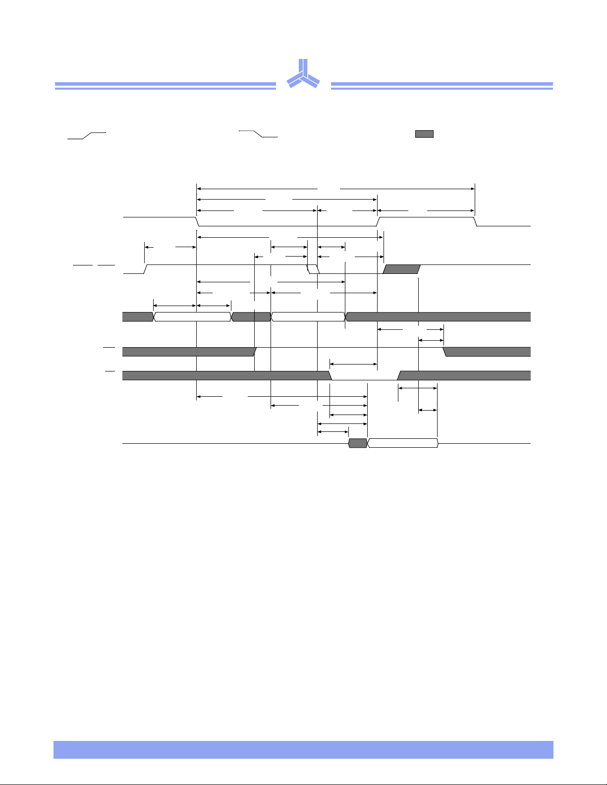
Key to switching waveforms
AS4C256K16FO
®
Rising input
Read cycle waveform
RAS
UCAS
, LCAS
t
ASR
Address
WE
OE
I/O
t
CRP
Row Address
t
RAD
t
RAC
t
t
RCD
RAH
t
ASC
t
AR
Falling input
t
RAS
t
CSH
t
RCS
Col Address
t
CLZ
Undefined/don’t care
t
RC
t
ROH
t
RRH
t
RP
t
RCH
t
OEZ
t
OFF
t
RSH
t
CAH
t
CAS
t
RAL
t
AA
t
t
OEA
CAC
Data Out
4/11/01; V.0.9.1 Alliance Semiconductor P. 7 of 25
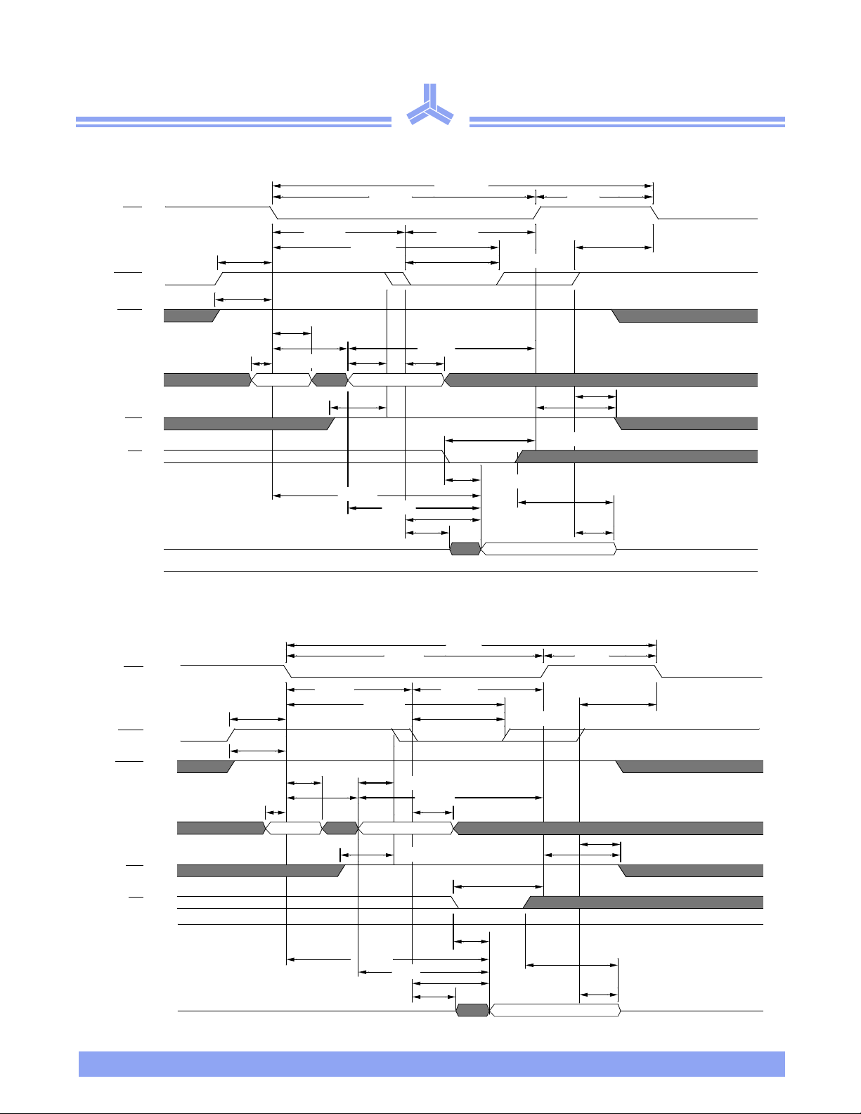
Upper byte read waveform
RAS
UCAS
LCAS
t
t
ASR
Address
WE
OE
Upper I/O
Lower I/O
t
RCD
t
CRP
t
CRP
t
RAH
RAD
t
ASC
Row Column
t
RCS
t
RAC
t
t
CLZ
CSH
AS4C256K16FO
®
t
t
RAL
RC
t
RSH
t
CAH
t
t
OEA
CAC
t
CAS
Data Out
t
ROH
t
RP
t
CRP
t
RCH
t
RRH
t
OEZ
t
OFF
t
RAS
t
AA
Lower byte read waveform
RAS
LCAS
UCAS
t
ASR
Address
WE
OE
Upper I/O
Lower I/O
t
RCD
t
CRP
t
CRP
t
RAH
t
RAD
Row Column
t
RAC
t
CSH
t
t
RAL
t
RSH
RC
t
CAH
t
t
OEA
CAC
t
CAS
t
ROH
t
RP
t
CRP
t
RCH
t
RRH
t
OEZ
t
OFF
t
RAS
t
ASC
t
RCS
t
AA
t
CLZ
Data Out
4/11/01; V.0.9.1 Alliance Semiconductor P. 8 of 25
 Loading...