

Alliance Semiconductor Corporation AS29LV800T-90SC, AS29LV800T-80TI, AS29LV800T-80TC, AS29LV800T-80SI, AS29LV800T-80SC Datasheet
...
March 2001
AS29LV800
®
3V 1M × 8/512K × 16 CMOS Flash EEPROM
Features
• Organization: 1M×8/512K×16
• Sector architecture
- One 16K; two 8K; one 32K; and fifteen 64K byte sectors
- One 8K; two 4K; one 16K; and fifteen 32K word sectors
- Boot code sector architecture—T (top) or B (bottom)
- Erase any combination of sectors or full chip
• Single 2.7-3.6V power supply for read/write operations
• Sector protection
• High speed 70/80/90/120 ns address access time
• Automated on-chip programming algorithm
- Automatically programs/verifies data at specified address
• Automated on-chip erase algorithm
- Automatically preprograms/erases chip or specified
sectors
• Hardware RESET pin
- Resets internal state machine to read mode
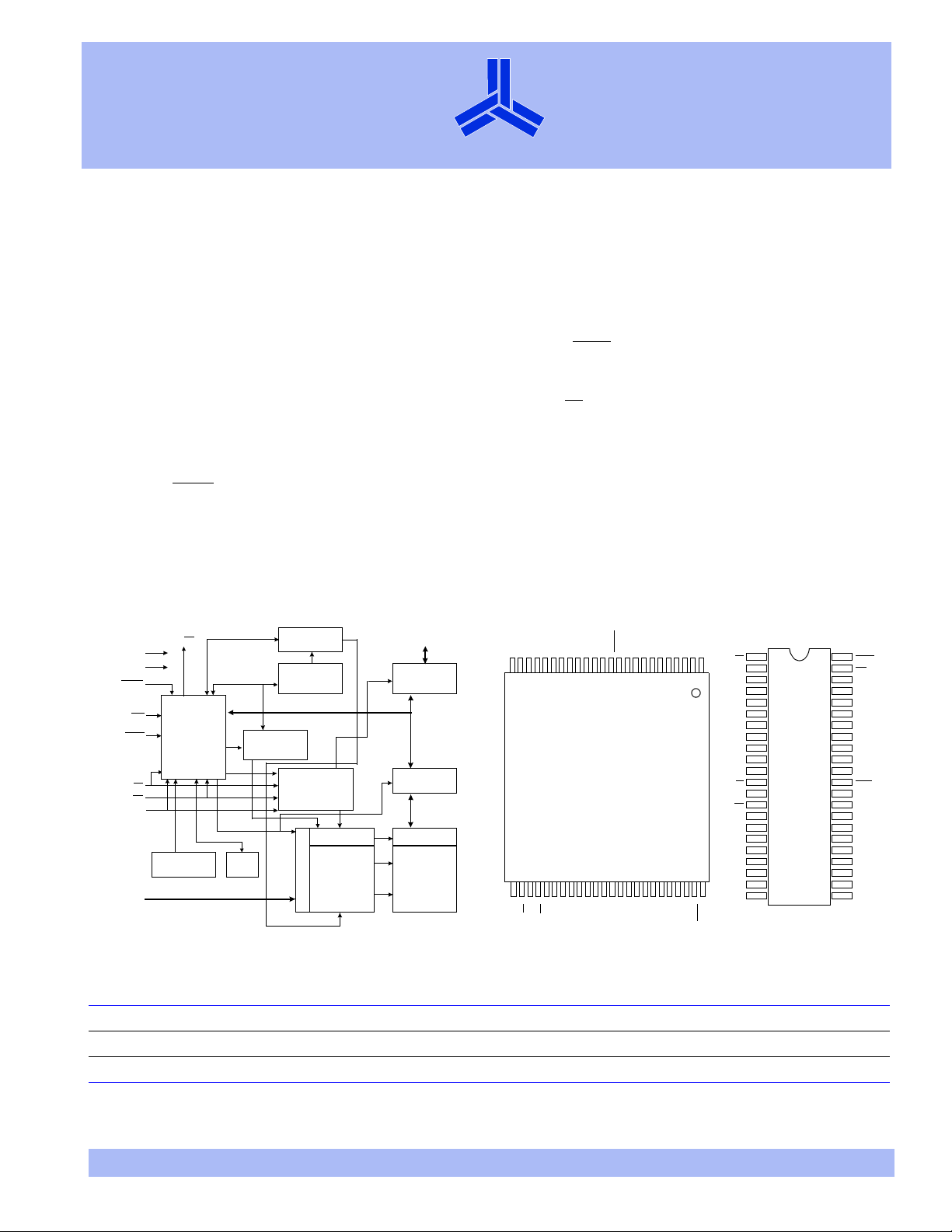
Logic block diagram
Sector protect/
V
RESET
BYTE
A-1
A0–A18
V
WE
OE
CC
SS
CE
RY/ BY
Program/erase
control
Command
register
VCC detector
Timer
erase voltage
Erase voltage
Program voltage
generator
Output enable
STB
switc hes
generator
Chip enable
Logic
Y decoder Y gating
X decoder
Address latch
STB
DQ0–DQ15
Input/output
buffers
Data latch
Cell matrix
• Low power consumption
- 200 nA typical automatic sleep mode current
- 200 nA typical standby current
- 10 mA typical read current
• JEDEC standard software, packages and pinouts
- 48-pin TSOP
- 44-pin SO; availability TBD
• Detection of program/erase cycle completion
- DQ7 DATA polling
- DQ6 toggle bit
- DQ2 toggle bit
-RY/BY
output
• Erase suspend/resume
- Supports reading data from or programming data to a
sector not being erased
•Low VCC write lock-out below 1.5V
• 10 year data retention at 150C
• 100,000 write/erase cycle endurance
Pin arrangement
DQ0
DQ8
DQ1
DQ9
DQ2
DQ10
DQ3
DQ11
A6
A5
A4
A3
A2
A1
A0
CE
V
SS
OE
44-pin SO
1RY/ B Y
2A18
3A17
4A7
5
6
7
8
9
10
11
12
13
AS29LV800
14
15
16
17
18
19
20
21
22
44
43
42
41
40
39
38
37
36
35
34
33
32
31
30
29
28
27
26
25
24
23
A1
22
23
24
27
26
25
A0CEVSSOE
A17
A7
A6A5A4A3A2
1718192021
3231302928
DQ0
DQ8
DQ1
DQ9
48-pin TSOP
RY/ B Y
RESET
A18
WE
NC
NC
NC
14
15
16
AS29LV800
35
34
33
DQ2
DQ10
DQ3
DQ11
VCCDQ4
DQ12
A10
A11
A12
A13
A14
NC
A8
A9
DQ5
DQ6
DQ13
A15
12345678910111213
48474645444342414039383736
A16
BYTE
V
DQ15/A-1
DQ7
DQ14
SS
RESET
WE
A8
A9
A10
A11
A12
A13
A14
A15
A16
BYTE
V
SS
DQ15/A-1
DQ7
DQ14
DQ6
DQ13
DQ5
DQ12
DQ4
V
CC
Selection guide
29LV800-70R
Maximum access time t
Maximum chip enable access time t
Maximum output enable access time t
AA
CE
OE
* Regulated voltage range of 3.0 to 3.6V
3/22/01; V.1.0 Alliance Semiconductor P. 1 of 25
70 80 90 120 ns
70 80 90 120 ns
30 30 35 50 ns
*
29LV800-80 29LV800-90 29LV800-120 Unit
Copyright © Alliance Semiconductor. All rights reserved.

March 2001
®
AS29LV800
Functional description
The AS29LV800 is an 8 megabit, 3.0 volt Flash memory organized as 1 Megabyte of 8 bits/512Kbytes of 16 bits each. For
flexible erase and program capability, the 8 megabits of data is divided into nineteen sectors: one 16K, two 8K, one 32K, and
fifteen 64k byte sectors; or one 8K, two 4K, one 16K, and fifteen 32K word sectors. The ×8 data appears on DQ0–DQ7; the
×16 data appears on DQ0–DQ15. The AS29LV800 is offered in JEDEC standard 48-pin TSOP and 44-pin SOP packages. This
device is designed to be programmed and erased in-system with a single 3.0V V
reprogrammed in standard EPROM programmers.
The AS29LV800 offers access times of 70/80/90/120 ns, allowing 0-wait state operation of high speed microprocessors. To
eliminate bus contention the device has separate chip enable (CE
mode (×16 output) is selected by BYTE
= high. Byte mode (×8 output) is selected by BYTE = low.
), write enable (WE), and output enable (OE) controls. Word
The AS29LV800 is fully compatible with the JEDEC single power supply Flash standard. Write commands are sent to the
command register using standard microprocessor write timings. An internal state-machine uses register contents to control the
erase and programming circuitry. Write cycles also internally latch addresses and data needed for the programming and erase
operations. Read data from the device occurs in the same manner as other Flash or EPROM devices. Use the program command
sequence to invoke the automated on-chip programming algorithm that automatically times the program pulse widths and
verifies proper cell margin. Use the erase command sequence to invoke the automated on-chip erase algorithm that
preprograms the sector (if it is not already programmed before executing the erase operation), times the erase pulse widths,
and verifies proper cell margin.
Boot sector architecture enables the system to boot from either the top (AS29LV800T) or the bottom (AS29LV800B) sector.
Sector erase architecture allows specified sectors of memory to be erased and reprogrammed without altering data in other
sectors. A sector typically erases and verifies within 1.0 seconds. Hardware sector protection disables both program and erase
operations in all, or any combination of, the nineteen sectors. The device provides true background erase with Erase Suspend,
which puts erase operations on hold to either read data from, or program data to, a sector that is not being erased. The chip
erase command will automatically erase all unprotected sectors.
A factory shipped AS29LV800 is fully erased (all bits = 1). The programming operation sets bits to 0. Data is programmed into
the array one byte at a time in any sequence and across sector boundaries. A sector must be erased to change bits from 0 to 1.
Erase returns all bytes in a sector to the erased state (all bits = 1). Each sector is erased individually with no effect on other
sectors.
The device features single 3.0V power supply operation for Read, Write, and Erase functions. Internally generated and
regulated voltages are provided for the Program and Erase operations. A low V
operations during power transtitions. The RY/BY
pin, DATA polling of DQ7, or toggle bit (DQ6) may be used to detect end of
program or erase operations. The device automatically resets to the read mode after program/erase operations are completed.
DQ2 indicates which sectors are being erased.
The AS29LV800 resists accidental erasure or spurious programming signals resulting from power transitions. Control register
architecture permits alteration of memory contents only after successful completion of specific command sequences. During
power up, the device is set to read mode with all program/erase commands disabled when V
voltage). The command registers are not affected by noise pulses of less than 5 ns on OE
commands, CE
When the device’s hardware RESET
state machine is reset to read mode. If the RESET
and WE must be logical zero and OE a logical 1.
pin is driven low, any program/erase operation in progress is terminated and the internal
pin is tied to the system reset circuitry and a system reset occurs during an
automated on-chip program/erase algorithm, data in address locations being operated on may become corrupted and requires
rewriting. Resetting the device enables the system’s microprocessor to read boot-up firmware from the Flash memory.
The AS29LV800 uses Fowler-Nordheim tunnelling to electrically erase all bits within a sector simultaneously. Bytes are
programmed one at a time using EPROM programming mechanism of hot electron injection.
supply. The device can also be
CC
detector automatically inhibits write
CC
is less than V
CC
(lockout
LKO
, CE, or WE. To initiate write
3/22/01; V.1.0 Alliance Semiconductor P. 2 of 25
March 2001
®
AS29LV800
Operating modes
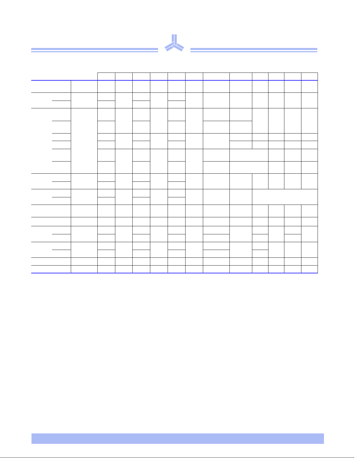
Mode CE OE WE A0 A1 A6 A9 RESET DQ
ID read MFR codeLLHLLLV
ID read device code L L H H L L V
ID
ID
Read L L H A0 A1 A6 A9 H D
Standby HXXXXXXHHigh Z
Output disable L HHXXXXHHigh Z
Write L H L A0 A1 A6 A9 H D
Enable sector protect L V
Sector unprotect L V
Temporary sector
unprotect
Verify sector protect
Verify sector unprotect
XXXXXXXV
†
LLHLHLVIDHCode
†
LLHLHHVIDHCode
ID
ID
Pulse/L L H L V
ID
Pulse/LL HHVIDHX
Hardware Reset XXXXXXXLHigh Z
L = Low (<VIL) = logic 0; H = High (>VIH) = logic 1; VID = 10.0 ± 1.0V; X = don’t care.
In ×16 mode, BYTE = V
†
Verification of sector protect/unprotect during A9 = V
. In ×8 mode, BYTE = VIL with DQ8-DQ14 in high Z and DQ15 = A-1.
IH
ID.
HCode
HCode
OUT
IN
HX
ID
X
Mode definitions
Item Description
ID MFR code,
device code
Read mode
Selected by A9 = V
When A0 is low (V
When A0 is high (V
Selected with CE
and t
after OE is low.
OE
Selected with CE
Standby
activated during an automated on-chip algorithm, the device completes the operation before entering
standby.
Output disable Part remains powered up; but outputs disabled with OE
Selected with CE
Write
register. Contents of command register serve as inputs to the internal state machine. Address latching occurs
on the falling edge of WE
whichever occurs first. Filters on WE
Enable
sector protect
Sector
unprotect
Ver if y se ct or
protect/
unprotect
Hardware protection circuitry implemented with external programming equipment causes the device to
disable program and erase operations for specified sectors. For in-system sector protection, refer to Sector
protect algorithm on page 14.
Disables sector protection for all sectors using external programming equipment. All sectors must be
protected prior to sector unprotection. For in-system sector unprotection, refer to Sector unprotect algorithm
on page 14.
Verifies write protection for sector. Sectors are protected from program/erase operations on commercial
programming equipment. Determine if sector protection exists in a system by writing the ID read command
sequence and reading location XXX02h, where address bits A12–18 select the defined sector addresses. A
logical 1 on DQ0 indicates a protected sector; a logical 0 indicates an unprotected sector.
(9.5V–10.5V), CE = OE = A1 = A6 = L, enabling outputs.
ID
) the output data = 52h, a unique Mfr. code for Alliance Semiconductor Flash products.
IL
IH
), D
represents the device code for the AS29LV800.
OUT
= OE = L, WE = H. Data is valid in t
= H. Part is powered down, and ICC reduced to <1.0 µA when CE = VCC ± 0.3V = RESET. If
= WE = L, OE = H. Accomplish all Flash erasure and programming through the command
or CE, whichever occurs later. Data latching occurs on the rising edge WE or CE,
prevent spurious noise events from appearing as write commands.
time after addresses are stable, tCE after CE is low
ACC
pulled high.
3/22/01; V.1.0 Alliance Semiconductor P. 3 of 25
March 2001
®
AS29LV800
Item Description
Te mp or ar y
sector
unprotect
RESET
Deep
power down
Automatic
sleep mode
Temporarily disables sector protection for in-system data changes to protected sectors. Apply +10V to RESET
to activate temporary sector unprotect mode. During temporary sector unprotect mode, program protected
sectors by selecting the appropriate sector address. All protected sectors revert to protected state on removal
of +10V from RESET
.
Resets the interal state machine to read mode. If device is programming or erasing when RESET = L, data
may be corrupted.
Hold RESET
low to enter deep power down mode (<1 µA). Recovery time to start of first read cycle is 50ns.
Enabled automatically when addresses remain stable for 300ns. Typical current draw is 1 µA. Existing data is
available to the system during this mode. If an address is changed, automatic sleep mode is disabled and new
data is returned within standard access times.
Flexible sector architecture
Bottom boot sector architecture (AS29LV800B) Top boot sector architecture (AS29LV800T)
Size
Sector
×8 ×16
(Kbytes) ×8 ×16
0 00000h–03FFFh 00000h–01FFFh 16 00000h–0FFFFh 00000h–07FFFh 64
1 04000h–05FFFh 02000h–02FFFh 8 10000h–1FFFFh 08000h–0FFFFh 64
2 06000h–07FFFh 03000h–03FFFh 8 20000h–2FFFFh 10000h–17FFFh 64
3 08000h–0FFFFh 04000h–07FFFh 32 30000h–3FFFFh 18000h–1FFFFh 64
4 10000h–1FFFFh 08000h–0FFFFh 64 40000h–4FFFFh 20000h–27FFFh 64
5 20000h–2FFFFh 10000h–17FFFh 64 50000h–5FFFFh 28000h–2FFFFh 64
6 30000h–3FFFFh 18000h–1FFFFh 64 60000h–6FFFFh 30000h–37FFFh 64
7 40000h–4FFFFh 20000h–27FFFh 64 70000h–7FFFFh 38000h–3FFFFh 64
8 50000h–5FFFFh 28000h–2FFFFh 64 80000h–8FFFFh 40000h–47FFFh 64
9 60000h–6FFFFh 30000h–37FFFh 64 90000h–9FFFFh 48000h–4FFFFh 64
10 70000h–7FFFFh 38000h–3FFFFh 64 A0000h–AFFFFh 50000h–57FFFh 64
11 80000h–8FFFFh 40000h–47FFFh 64 B0000h–BFFFFh 58000h–5FFFFh 64
12 90000h–9FFFFh 48000h–4FFFFh 64 C0000h–CFFFFh 60000h–67FFFh 64
13 A0000h–AFFFFh 50000h–57FFFh 64 D0000h–DFFFFh 68000h–6FFFFh 64
14 B0000h–BFFFFh 58000h–5FFFFh 64 E0000h–EFFFFh 70000h–77FFFh 64
15 C0000h–CFFFFh 60000h–67FFFh 64 F0000h–F7FFFh 78000h–7BFFFh 32
16 D0000h–DFFFFh 68000h–6FFFFh 64 F8000h–F9FFFh 7C000h–7CFFFh 8
17 E0000h–EFFFFh 70000h–77FFFh 64 FA000h–FBFFFh 7D000h–7DFFFh 8
18 F0000h–FFFFFh 78000h–7FFFFh 64 FC000h–FFFFFh 7E000h–7FFFFh 16
In word mode, there are one 8K word, two 4K word, one 16K word, and fifteen 32K word sectors. Address range is A18–A-1 if BYTE = VIL; address range is
A18–A0 if BYTE
= VIH.
Size
(Kbytes)
3/22/01; V.1.0 Alliance Semiconductor P. 4 of 25

March 2001
®
AS29LV800
ID Sector address table
Bottom boot sector address
(AS29LV800B)
Sector
0 000000X 00 0 0XXX
1 0000010 000 1 XXX
2 0000011 001 0 XXX
3 00001XX 0 0 1 1XXX
4 0001XXX 0100XXX
5 0010XXX 0101XXX
6 0011XXX 0110XXX
7 0100XXX 0111XXX
8 0101XXX 1000XXX
9 0110XXX 1001XXX
10 0111XXX 10 1 0XXX
11 1000XXX 10 1 1XXX
12 1001XXX 11 0 0XXX
13 1010XXX 11 0 1XXX
14 1011XXX 11 1 0XXX
15 1100XXX 11 1 1 0 XX
16 1101XXX 1111100
17 1110XXX 1111101
18 1111XXX 11 1 1 1 1X
A18 A17 A16 A15 A14 A13 A12 A18 A17 A16 A15 A14 A13 A12
Top boot sector address
(AS29LV800T)
READ codes
Mode A18–A12 A6 A1 A0 Code
MFR code (Alliance Semiconductor) X L L L 52h
×8 T boot X L L H DAh
Device code
Sector protection Sector address L H L
Key: L =Low (<VIL); H = High (>VIH); X =Don’t care
3/22/01; V.1.0 Alliance Semiconductor P. 5 of 25
×8 B boot X L L H 5Bh
×16 T boot X L L H 22DAh
×16 B boot X L L H 225Bh
01h protected
00h unprotected
March 2001
®
Command format
Required bus
Command sequence
Reset/Read 1 XXXh F0h
Reset/Read
Autoselect
ID Read
Program
Unlock bypass
Unlock bypass program 2 XXX A0h
Unlock bypass reset 2 XXX 90h XXX 00h
Chip Erase
Sector Erase
Sector Erase Suspend 1 XXXh B0h
Sector Erase Resume 1 XXXh 30h
×16
×8 AAAh 555h AAAh
×16
×8 AAAh 555h AAAh
×16 555h
×8 AAAh 555h AAAh 52h
×16 555h
×8 AAAh 555h AAAh
×16
×8 AAAh 555h AAAh
×16
×8 AAA 555 AAA
×16
×8 AAAh 555h AAAh AAAh 555h AAAh
×16
×8 AAAh 555h AAAh AAAh 555h
write cycles
3
3
4
3
6
6
1 Bus operations defined in "Mode definitions," on page 3.
2 Reading from and programming to non-erasing sectors allowed in Erase Suspend mode.
3 Address bits A11-A18 = X = Don’t Care for all address commands except where Program Address and Sector Address are required.
4 Data bits DQ15-DQ8 are don’t care for unlock and command cycles.
5 The Unlock Bypass command must be initiated before the Unlock Bypass Program command.
6 The Unlock Bypass Reset command returns the device to reading array data when it is in the unlock bypass mode.
1st bus cycle 2nd bus cycle 3rd bus cycle 4th bus cycle 5th bus cycle 6th bus cycle
Address Data Address Data Address Data Address Data Address Data Address Data
Read
Read Data
Address
555h
555h
555h
555
555h
555h
AAh
AAh
AAh
AAh
AAh
AAh
AAh
AAh
2AAh
2AAh
2AAh
2AAh
2AAh
2AA
Program
address
2AAh
2AAh
55h
55h
55h
55h
55h
55h
Program
data
55h
55h
555h
555h
555h
555h
555h
555
555h
555h
F0h Read Address
01h
90h
90h
90h
A0h Program Address Program Data
20h
80h
80h
Device code
02h
Device code
00h
MFR code
XXX02h
Sector protection
XXX04h
Sector protection
555h
555h
Read
Data
22DAh (T)
225Bh (B)
DAh (T) 5Bh
(B)
0052h
0001h = protected
0000h = unprotected
0001h=protected
0000h=unprotected
AAh
AAh
2AAh
2AAh
AS29LV800
555h
55h
Sector
55h
Address
10h
30h
3/22/01; V.1.0 Alliance Semiconductor P. 6 of 25

March 2001
Command definitions
Item Description
Initiate read or reset operations by writing the Read/Reset command sequence into the command
register. This allows the microprocessor to retrieve data from the memory. Device remains in read
Reset/Read
mode until command register contents are altered.
Device automatically powers up in read/reset state. This feature allows only reads, therefore
ensuring no spurious memory content alterations during power up.
AS29LV800 provides manufacturer and device codes in two ways. External PROM programmers
typically access the device codes by driving +10V on A9. AS29LV800 also contains an ID Read
command to read the device code with only +3V, since multiplexing +10V on address lines is
generally undesirable.
AS29LV800
®
ID Read
Hardware Reset
Byte/word
Programming
Initiate device ID read by writing the ID Read command sequence into the command register.
Follow with a read sequence from address XXX00h to return MFR code. Follow ID Read command
sequence with a read sequence from address XXX01h to return device code.
To verify write protect status on sectors, read address XXX02h. Sector addresses A18–A12 produce
a 1 on DQ0 for protected sector and a 0 for unprotected sector.
Exit from ID read mode with Read/Reset command sequence.
Holding RESET
handled in the operation is corrupted. The internal state machine resets 20 µs after RESET
low. RY/BY
of 50 ns for the device to permit read operations.
Programming the AS29LV800 is a four bus cycle operation performed on a byte-by-byte or wordby-word basis. Two unlock write cycles precede the Program Setup command and program data
write cycle. Upon execution of the program command, no additional CPU controls or timings are
necessary. Addresses are latched on the falling edge of CE
on the rising edge of CE
algorithm provides adequate internally-generated programming pulses and verifies the
programmed cell margin.
Check programming status by sampling data on the RY/BY
or toggle bit (DQ6) at the program address location. The programming operation is complete if
DQ7 returns equivalent data, if DQ6 = no toggle, or if RY/BY
The AS29LV800 ignores commands written during programming. A hardware reset occurring
during programming may corrupt the data at the programmed location.
low for 500 ns resets the device, terminating any operation in progress; data
is driven
remains low until internal state machine resets. After RESET is set high, there is a delay
or WE, whichever is last; data is latched
or WE, whichever is first. The AS29LV800’s automated on-chip program
pin, or either the DATA polling (DQ7)
pin = high.
AS29LV800 allows programming in any sequence, across any sector boundary. Changing data from
0 to 1 requires an erase operation. Attempting to program data 0 to 1 results in either DQ5 = 1
(exceeded programming time limits); reading this data after a read/reset operation returns a 0.
When programming time limit is exceeded, DQ5 reads high, and DQ6 continues to toggle. In this
state, a Reset command returns the device to read mode.
3/22/01; V.1.0 Alliance Semiconductor P. 7 of 25

March 2001
Item Description
The unlock bypass feature increases the speed at which the system programs bytes or words to the
device because it bypasses the first two unlock cycles of the standard program command sequence.
To initiate the unlock bypass command sequence, two unlock cycles must be written, then
followed by a third cycle which has the unlock bypass command, 20h.
The device then begins the unlock bypass mode. In order to program in this mode, a two cycle
Unlock Bypass
Command Sequence
unlock bypass program sequence is required. The first cycle has the unlock bypass program
command, A0h. It is followed by a second cycle which has the program address and data. To
program additional data, the same sequence must be followed.
The unlock bypass mode has two valid commands, the Unlock Bypass Program command and the
Unlock Bypass Reset command. The only way the system can exit the unlock bypass mode is by
issuing the unlock bypass reset command sequence. This sequence involves two cycles. The first
cycle contains the data, 90h. The second cycle contains the data 00h. Addresses are don’t care for
both cycles. The device then returns to reading array data.
Chip erase requires six bus cycles: two unlock write cycles; a setup command, two additional
unlock write cycles; and finally the Chip Erase command.
AS29LV800
®
Chip Erase
Sector Erase
Chip erase does not require logical 0s to be written prior to erasure. When the automated on-chip
erase algorithm is invoked with the Chip Erase command sequence, AS29LV800 automatically
programs and verifies the entire memory array for an all-zero pattern prior to erase. The 29LV800
returns to read mode upon completion of chip erase unless DQ5 is set high as a result of exceeding
time limit.
Sector erase requires six bus cycles: two unlock write cycles, a setup command, two additional
unlock write cycles, and finally the Sector Erase command. Identify the sector to be erased by
addressing any location in the sector. The address is latched on the falling edge of WE
command, 30h is latched on the rising edge of WE
erase time-out.
To erase multiple sectors, write the Sector Erase command to each of the addresses of sectors to
erase after following the six bus cycle operation above. Timing between writes of additional sectors
must be less than the erase time-out period, or the AS29LV800 ignores the command and erasure
begins. During the time-out period any falling edge of WE
(other than Sector Erase or Erase Suspend) during time-out period resets the AS29LV800 to read
mode, and the device ignores the sector erase command string. Erase such ignored sectors by
restarting the Sector Erase command on the ignored sectors.
The entire array need not be written with 0s prior to erasure. AS29LV800 writes 0s to the entire
sector prior to electrical erase; writing of 0s affects only selected sectors, leaving non-selected
sectors unaffected. AS29LV800 requires no CPU control or timing signals during sector erase
operations.
Automatic sector erase begins after sector erase time-out from the last rising edge of WE
sector erase command stream and ends when the DATA
address must be performed on addresses that fall within the sectors being erased. AS29LV800
returns to read mode after sector erase unless DQ5 is set high by exceeding the time limit.
. The sector erase operation begins after a sector
resets the time-out. Any command
polling (DQ7) is logical 1. DATA polling
; the
from the
3/22/01; V.1.0 Alliance Semiconductor P. 8 of 25
 Loading...