

Alliance Semiconductor P2781, P2782, P2784 Service Manual

July 2005 P2781/82/84
rev 1.5
General Purpose EMI Reduction IC
Features
Provides up to 15dB of EMI suppression
FCC approved method of EMI attenuation
Generates a 1X, 2X, and 4X low EMI spread
spectrum clock of the input frequency
Input frequency range from 3 to 78MHz
External loop filter for spread % adjustment
Spreading ranges from ±0.25% to ±5.0%
Ultra low cycle-to-cycle jitter
Zero-cycle slip
3.3V operating voltage range
10 mA output drives
TTL or CMOS compatible outputs
Ultra-low power CMOS design
P278XA is available in 8 pin SOIC and TSSOP
Packages
Available for industrial and automotive
temperature ranges.
Product Description
The P278xA is a versatile spread spectrum frequency
modulator designed specifically for digital camera and
other digital video and imaging applications. The P278xA
reduces electromagnetic interference (EMI) at the clock
source, which provides system wide reduction of EMI of
all clock dependent signals. The P278xA allows
significant system cost savings by reducing the number of
circuit board layers and shielding that are traditionally
required to pass EMI regulations.
The P278xA uses the most efficient and optimized
modulation profile approved by the FCC. The P278xA
modulates the output of a single PLL in order to “spread”
the bandwidth of a synthesized clock and, more
importantly, decreases the peak amplitudes of its
harmonics. This results in significantly lower system EMI
compared to the typical narrow band signal produced by
oscillators and most frequency generators. Lowering EMI
by increasing a signal’s bandwidth is called spread
spectrum clock generation.
Applications
The P278xA is targeted towards MFP, xDSL, fax modem,
set-top box, USB controller, DSC, and embedded systems.
Block Diagram
XIN /CLKIN
XOUT
Crystal
Oscillator
Frequency
Divider
Feedback
Divider
FS0
Phase
Detector
FS1
LF
VCO
VDD
PLL
Output
Divider
ModOUT
VSS
Alliance Semiconductor
2575, Augustine Drive • Santa Clara, CA • Tel: 408.855.4900 • Fax: 408.855.4999 • www.alsc.com
Notice: The information in this document is subject to change without notice.
July 2005
P2781/82/84
rev 1.5
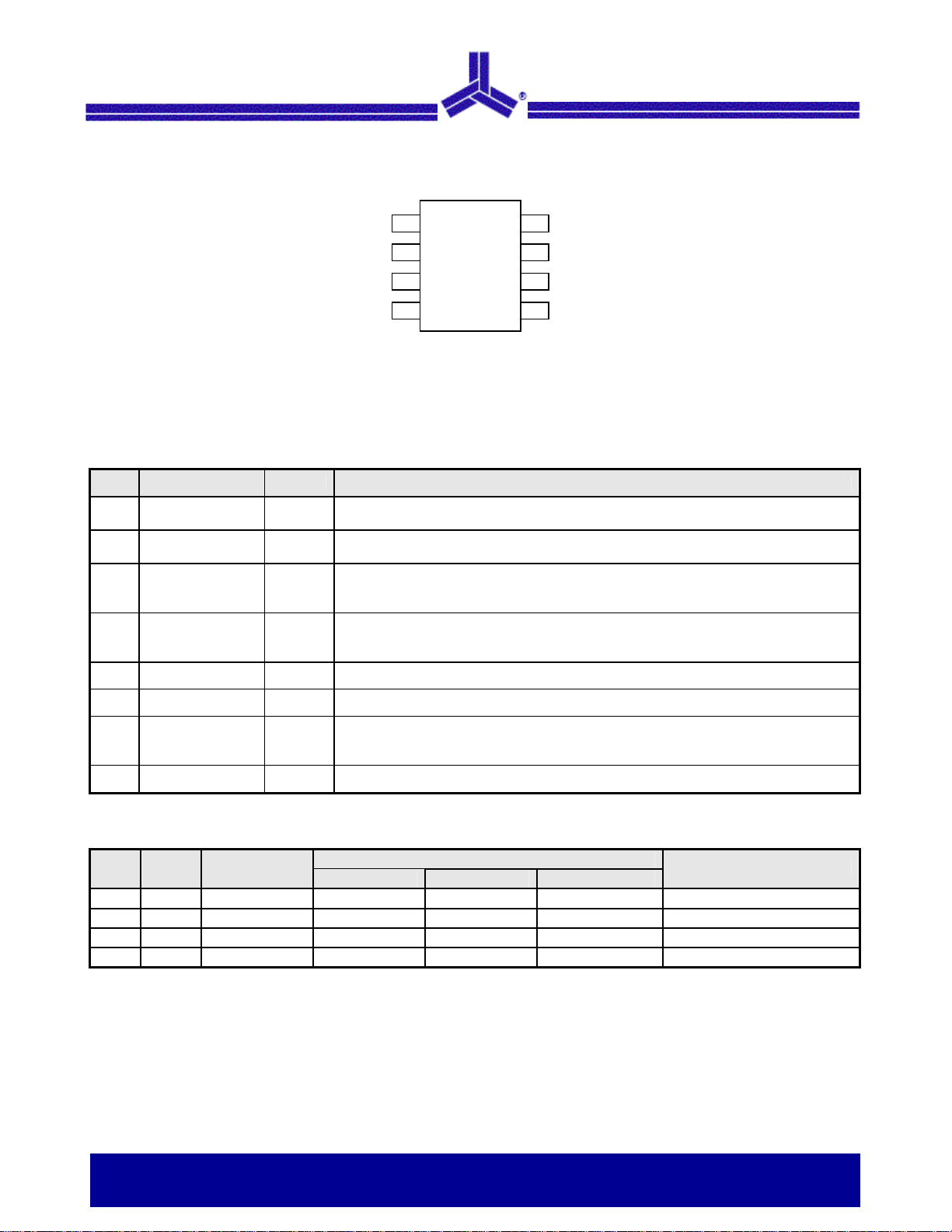
Pin Configuration
Pin Description (P278XA)
Pin# Pin Name Type Description
1 XIN/CLKIN I
2 XOUT O
3 FS1 I
4 LF I
5 VSS I Ground Connection. Connect to system ground.
XIN / CLKIN
XOUT
FS1
Connect to crystal or clock input. This pin has dual functions. It can be connected
either to an external crystal or an external reference clock.
Crystal connection. If using an external reference, this pin must be left
unconnected.
Digital logic input used to select input frequency range
(see the Input Frequency Selection Table). This pin has an internal pull-up
resistor.
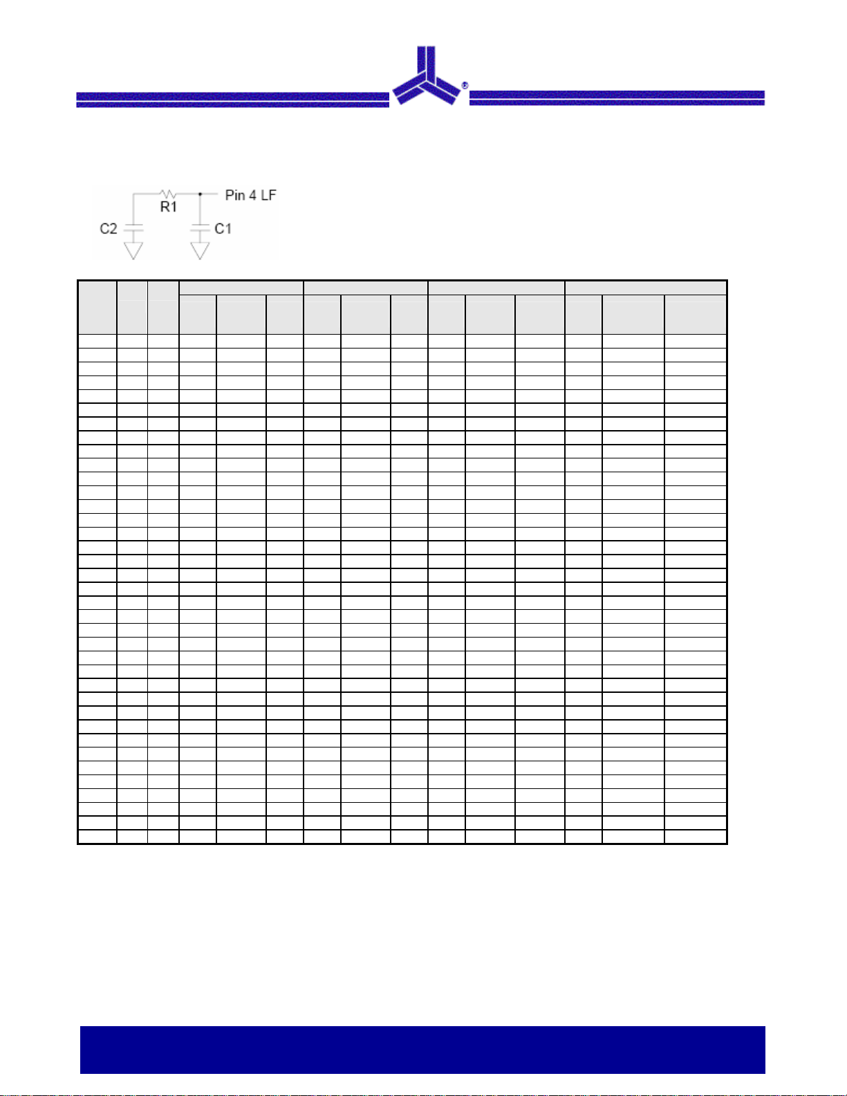
External Loop Filter for the PLL. By changing the value of the CRC circuit, the
percentage spread can be adjusted accordingly. See the Loop Filter Selection
Table for detail value.
1
2
P278XA-08S
P278XA-08T
3
4
LF
Standard pin Configuration offered in both
8 pin SOIC and TSSOP Packages
8
7
6
5
VDD
FS0
ModOUT
VSS
6 ModOUT O Spread Spectrum Clock Output.
Digital logic input used to select input frequency range
7 FS0 I
8 VDD P Connect to +3.3 V
(see the Input Frequency Selection Table). This pin has an internal pull-up
resistor.
Input Frequency Selection Table
FS1 FS0 Input (MHz)
0 0 3 to 9 3 to 9 6 to 18 12 to 36 Fin / 128
0 1 10 to 19 10 to 19 20 to 38 40 to 76 Fin / 256
1 0 20 to 38 20 to 38 40 to 76 80 to 152 Fin / 512
1 1 39 to 78 39 to 78 78 to 156 156 to 312 Fin / 1024
Output Frequency Scaling (MHz)
P2781A P2782A P2784A
Modulation Rate (KHz)
General Purpose EMI Reduction IC 2 of 11
Notice: The information in this document is subject to change without notice.
July 2005
P2781/82/84
rev 1.5
Loop Filter Selection Table VDD 3.3V
Contact Alliance for loop values that are not listed in the table and for component
selection values for industrial and automotive temperatures.
Input
FS1 FS0
MHz
3 0 0 270 330,000 220 270 330,000 300 270 100,000 390 560 100,000 510
4 0 0 270 100,000 270 270 100,000 390 270 100,000 560 560 100,000 680
5 0 0 270 100,000 390 270 100,000 560 270 100,000 750 560 100,000 910
6 0 0 270 100,000 510 270 100,000 750 270 10,000 1,000 680 6,800 1,200
7 0 0 270 100,000 620 270 100,000 1,000 270 5,600 1,200 330 3,300 1,200
8 0 0 270 100,000 820 270 100,000 1,200 270 12,000 2,200 680 6,800 2,200
9 0 0 270 100,000 1,000 270 100,000 1,500 270 5,600 2,200 270 2,700 2,200
10 0 1 270 100,000 330 270 100,000 510 270 100,000 750 560 100,000 910
11 0 1 270 100,000 390 270 100,000 560 270 100,000 866(1%) 560 100,000 1,100
12 0 1 270 100,000 510 270 100,000 750 270 10,000 1,000 680 6,800 1,200
13 0 1 270 100,000 560 270 100,000 820 270 12,000 1,200 470 4,700 1,200
14 0 1 270 100,000 620 270 100,000 1,000 270 5,600 1,200 330 3,300 1,200
15 0 1 270 100,000 750 270 100,000 1,100 270 3,900 1,200 330 3,300 1,500
16 0 1 270 100,000 820 270 100,000 1,200 270 12,000 2,200 680 6,800 2,200
17 0 1 270 100,000 910 270 100,000 1,300 270 10,000 2,200 390 3,900 2,200
18 0 1 270 100,000 1,000 270 100,000 1,500 270 5,600 2,200 270 2,700 2,200
19 0 1 270 100,000 1,200 270 100,000 1,600 270 3,300 2,200 270 2,700 2,700
20 0 0 270 100,000 330 270 100,000 560 270 100,000 750 560 100,000 910
21-22 1 0 270 100,000 390 270 100,000 620 270 100,000 866 (1%) 560 100,000 1,100
23-24 1 0 270 100,000 510 270 100,000 750 270 10,000 1,000 680 6,800 1,200
25-26 1 0 270 100,000 560 270 100,000 820 270 12,000 1,200 470 4,700 1,200
27-28 1 0 270 100,000 620 270 100,000 1,000 270 6,800 1,200 330 3,300 1,200
29-30 1 0 270 100,000 750 270 100,000 1,100 270 3,900 1,200 330 3,300 1,500
31-32 1 0 270 100,000 820 270 100,000 1,200 270 12,000 2,200 680 6,800 2,200
33-34 1 0 270 100,000 910 270 100,000 1,300 270 10,000 2,200 390 3,900 2,200
35-36 1 0 270 100,000 1,000 270 100,000 1,500 270 5,600 2,200 270 2,700 2,200
37-38 1 0 270 100,000 1,200 270 100,000 1,600 270 3,300 2,200 270 2,700 2,700
39-42 1 1 270 100,000 330 270 100,000 560 270 100,000 750 560 100,000 910
43-46 1 1 270 100,000 390 270 100,000 620 270 100,000 866 (1%) 560 100,000 1,100
47-50 1 1 270 100,000 510 270 100,000 750 270 10,000 1,000 680 6,800 1,200
51-54 1 1 270 100,000 560 270 100,000 820 270 12,000 1,200 470 4,700 1,200
55-58 1 1 270 100,000 620 270 100,000 1,000 270 6,800 1,200 330 3,300 1,200
59-62 1 1 270 100,000 750 270 100,000 1,100 270 3,900 1,200 330 3,300 1,500
63-66 1 1 270 100,000 820 270 100,000 1,200 270 12,000 2,200 680 6,800 2,200
67-70 1 1 270 100,000 910 270 100,000 1,300 270 8,200 2,200 390 3,900 2,200
71-74 1 1 270 100,000 1,000 270 100,000 1,600 270 5,600 2,200 270 2,700 2,200
75-78 1 1 270 100,000 1,200 270 100,000 1,800 270 3,300 2,200 270 2,700 2,700
1 The BW value is representative of typical conditions
BW = ±0.50%1 BW = ±0.75%1 BW = ±1.00%1 BW = ±1.25%1
C1
(pF)
C2
(pF)
R1
(ohm)
C1
(pF)
C2
(pF)
R1
(ohm)
C1
(pF)
C2
(pF)
R1
(ohm)
C1
(pF)
C2
(pF)
R1
(ohm)
General Purpose EMI Reduction IC 3 of 11
Notice: The information in this document is subject to change without notice.
July 2005
P2781/82/84
rev 1.5
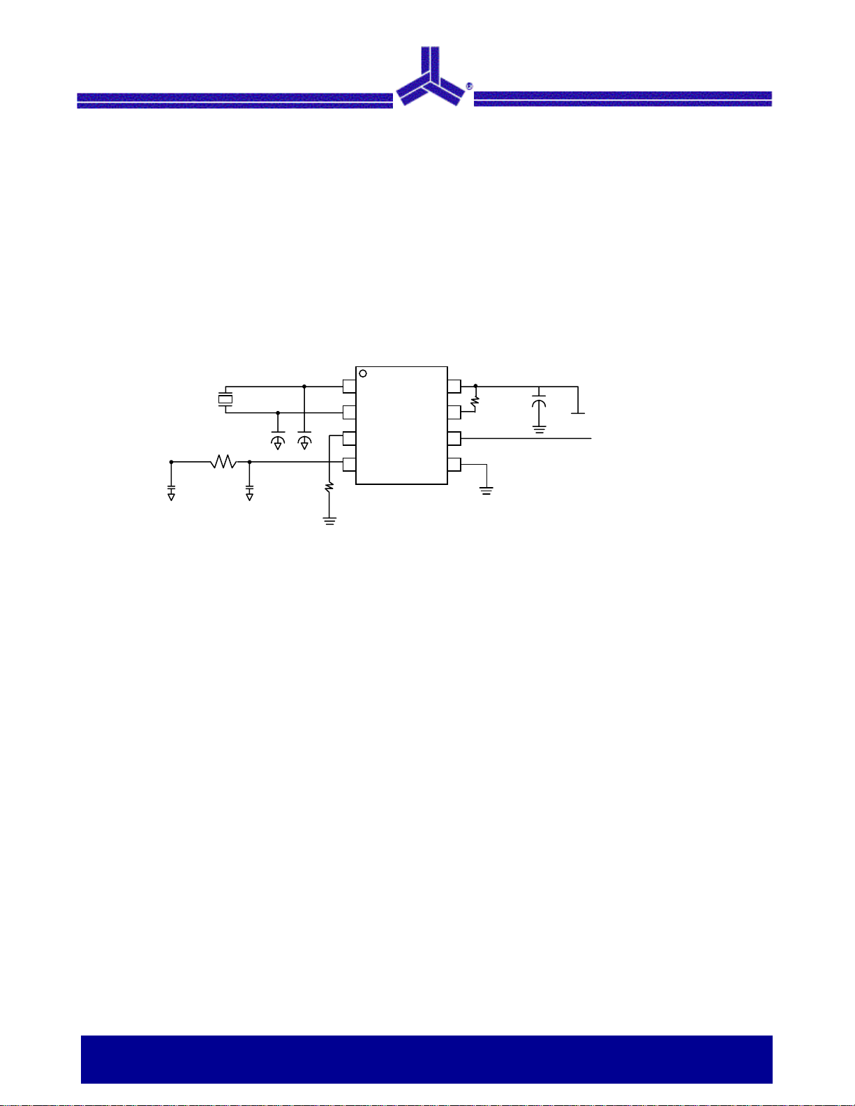
Spread Spectrum Selection
The P278xA performs Zero Cycle Slip when set at low percentage spreading. This allows no occurrence of system timing
error. The optimal setting should minimize system EMI to the fullest without affecting system performance. The spreading is
described as a percentage deviation of the center frequency.
(Note: the center frequency is the frequency of the external reference input on CLKIN, Pin 1.)
The P2781A is designed for PC peripheral, networking, notebook PC, and LCD monitor applications. It is optimized for
operation between 3 to 78MHz range. In the following application schematic example, the P2781A spread percentage
selection is determined by the external LF value specified in the Loop Filter Selection Table. The Input Frequency Selection
Table specifies the input frequency range. The external LF allows the user to fine tune the spread percentage to optimize the
EMI reduction benefits of the spread spectrum.
C2 C1
Note: Both logic input pins FS1 and FS0 have to be connected to either VDD or VSS. Do not leave them floating.
16 MHz
R1
0 Ohm
XIN/CLKIN
1
XOUT
2
FS1
3
4
ModOUT
P2781A
VDD
FS0
VSSLF
8
2.2 K
7
6
5
0.1µF
+3.3V
Modulated 16MHz Clock
To target Chip
General Purpose EMI Reduction IC 4 of 11
Notice: The information in this document is subject to change without notice.
 Loading...