

Alliance Semiconductor P2681A Service Manual
查询P2681A供应商
October 2003 P2681A
rev D
General Purpose EMI Reduction IC
Features
FCC approved method of EMI attenuation
Provides up to 15 dB of EMI suppression
Generates a 1 X or ½ X low EMI spread
spectrum clock of the input frequency
Output frequency from 6MHz to 20MHz
Digital spread selections
Spreading ranges from +/-0.4% to +/-5.0%
Ultra low cycle-to-cycle jitter
Zero-cycle slip
3.3V and 5.0V operating voltage range
10 mA output drives
TTL or CMOS compatible outputs
Ultra-low power CMOS design
Available in 8 pin SOIC and TSSOP
Product Description
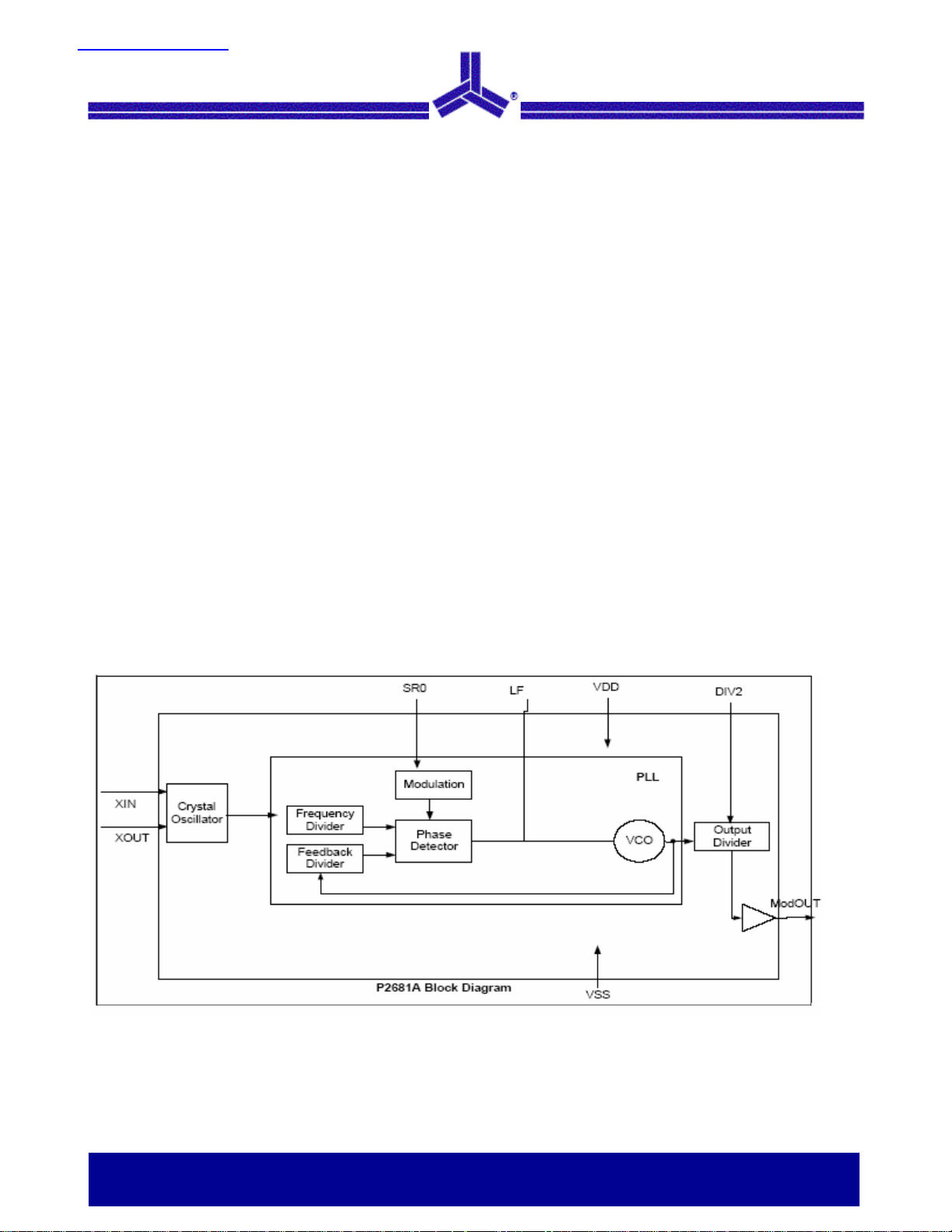
The P2681A is a versatile spread spectrum
frequency modulator designed specifically for digital
camera and other digital video and imaging
applications. The P2681A reduces electromagnetic
interference (EMI) at the clock source, which
provides system wide reduction of EMI of all clock
dependent signals. The P2681A allows significant
Block Diagram
system cost savings by reducing the number of circuit
board layers and shielding that are traditionally
required to pass EMI regulations.
The P2681A uses the most efficient and optimized
modulation profile approved by the FCC.
The P2681A modulates the output of a single PLL in
order to “spread” the bandwidth of a synthesized
clock and, more importantly, decreases the peak
amplitudes of its harmonics. This results in
significantly lower system EMI compared to the
typical narrow band signal produced by oscillators
and most frequency generators. Lowering EMI by
increasing a signal’s bandwidth is called “spread
spectrum clock generation”.
Applications
The P2681A is targeted towards MFP, xDSL, fax
modem, set-top box, USB controller, DSC, and
embedded systems.
2575, Augustine Drive • Santa Clara, CA • Tel: 408.855.4900 • Fax: 408.855.4999 • www.alsc.com
Notice: The information in this document is subject to change without notice.
Alliance Semiconductor

October 2003 P2681A
rev D
Pin Configuration
Pin Description
Pin# Pin Name Type Description
1 XIN/CLKIN I Connect to crystal or clock input.
2 XOUT I Crystal output
Digital logic input used to select normal output mode or divide-by-2 output
3 DIV2 I
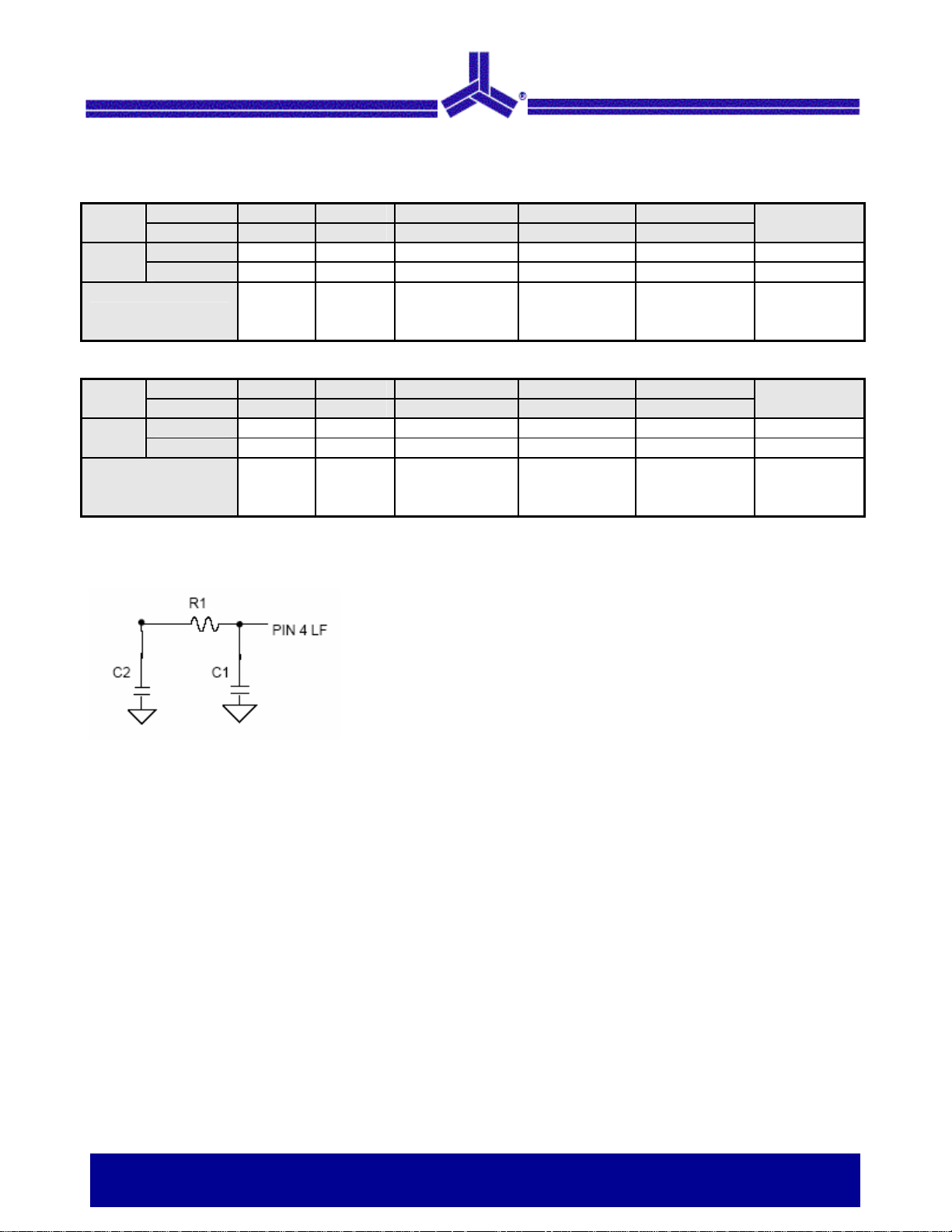
4 LF I
5 VSS I Ground Connection. Connect to system ground.
6 ModOUT O Spread Spectrum Clock Output.
7 SR0 I
8 VDD P Connect to +3.3V or 5.0V
mode. When this pin is Low, the frequency of the output clock is the same
as the input clock frequency. When it is tied High, the output frequency is
half the input clock frequency. This pin has an internal pull-low resistor.
External Loop Filter for the PLL. By changing the value of the CRC circuit,
the % spread can be adjusted accordingly. See Table 1.2 for detail value.
Digital logic input used to select Spreading Range between large or small
for a given LF value (see Table 1.1 and 1.2). When SR0=0, the spreading %
is smaller than SR0=1. This pin has an internal pull-up resistor.
Notice: The information in this document is subject to change without notice.
General Purpose EMI Reduction IC 2 of 10
October 2003 P2681A
rev D
Table 1 - Modulation Output and Spreading Selection VDD @ 3.3V
DIV=0
SR0
Loop filter value*
DIV=0
SR0
Loop filter value*
*For additional spread % selection please refer to Loop Filter Selection Table
Table 2 - Loop Filter Selection Table VDD @ 3.3V
Xin 6 MHz 8 MHz 10 MHz 12 MHz 16 MHz
ModOut 6 MHz 8 MHz 10 MHz 12 MHz 16 MHz
0
1
Xin 6 MHz 8 MHz 10 MHz 12 MHz 16 MHz
ModOut 3 MHz 4 MHz 5 MHz 6 MHz 8 MHz
0
1
TBD TBD +/-0.75% +/-0.75% +/-0.75% ModOut/256
TBD TBD +/-1.30% +/-1.30% +/-1.30% ModOut/256
C1=1,000 pF
TBD TBD
TBD TBD +/-0.75% +/-0.75% +/-0.75% ModOut/128
TBD TBD +/-1.30% +/-1.30% +/-1.30% ModOut/128
TBD TBD
C2=10,000 pF
R1=1K
C1=1,000 pF
C2=10,000 pF
R1=1K
C1=1,000 pF
C2=10,000 pF
R1=1.5K
C1=1,000 pF
C2=10,000 pF
R1=1.5K
C1=390 pF
C2=3,900 pF
R1=2.2K
C1=390 pF
C2=3,900 pF
R1=2.2K
Modulation
Rate
Modulation
Rate
Please contact Alliance Semiconductor for more information
General Purpose EMI Reduction IC 3 of 10
Notice: The information in this document is subject to change without notice.
 Loading...