

Alliance Semiconductor ASMP5P23S09A, ASMP5P23S05A Service Manual
Alliance Semiconductor
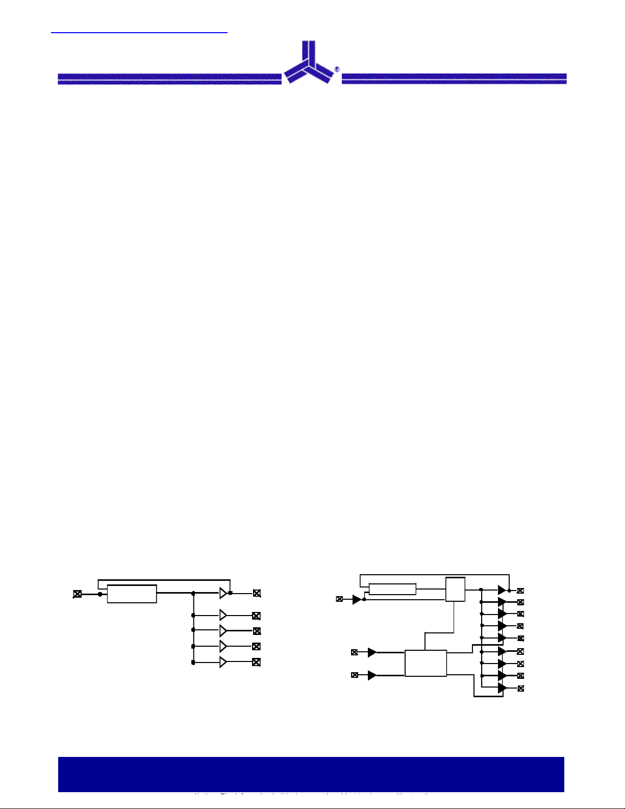
PLL
CLKOUT
CLK1
CLK2
CLK3
CLK4
REF
CLKA2
CLKA3
CLKA4
S1
MUX
查询ASM5I23S09A-1-16-SR供应商
ASMP5P23S09A
August 2004 ASMP5P23S05A
rev 2.0
3.3V ‘SpreadTrak’ Zero Delay Buffer
General Features
10 MHz to 133- MHz operating range, compatible
with CPU and PCI bus frequencies.
Zero input - output propagation delay.
Multiple low-skew outputs.
Output-output skew less than 250 ps.
Device-device skew less than 700 ps.
One input drives 9 outputs, grouped as 4 + 4
+ 1 (ASM5P23S09A).
One input drives 5 outputs (ASM5P23S05A).
Less than 200 ps cycle-to-cycle jitter is compatible
with Pentium®based systems.
Test Mode to bypass PLL (ASM5P23S09A only,
refer Select Input Decoding Table).
Available in 16-pin, 150-mil SOIC, 4.4 mm
TSSOP, and 150-mil SSOP packages
(ASM5P23S09A) or in 8-pin, 150-mil SOIC
package (ASM5P23S05A).
3.3V operation, advanced 0.35µ CMOS
technology.
‘SpreadTrak’.
133- MHz frequencies, and has higher drive than the -1
devices. All parts have on-chip PLLs that lock to an input
clock on the REF pin. The PLL feedback is on-chip and is
obtained from the CLKOUT pad.
The ASM5P23S09A has two banks of four outputs each,
which can be controlled by the Select inputs as shown in
the Select Input Decoding Table. If all the output clocks are
not required, Bank B can be three-stated. The select input
also allows the input clock to be directly applied to the
outputs for chip and system testing purposes.
Multiple ASM5P23S09A and ASM5P23S05A devices can
accept the same input clock and distribute it. In this case
the skew between the outputs of the two devices is
guaranteed to be less than 700ps.
All outputs have less than 200 ps of cycle-to-cycle jitter.
The input and output propagation delay is guaranteed to be
less than 250 ps, and the output to output skew is
guaranteed to be less than 250ps.
Functional Description
ASM5P23S09A is a versatile, 3.3V zero-delay buffer
designed to distribute high-speed clocks with Spread
Spectrum capability. It is available in a 16-pin package. The
ASM5P23S05A is the eight-pin version of the
ASM5P23S09A. It accepts one reference input and drives
out five low-skew clocks.
The -1H version of the ASM5P23SXXA operates at up to
Block Diagram
ASM5P23S05A
The ASM5P23S09A and the ASM5P23S05A are available
in two different configurations, as shown in the ordering
information table. The ASM5P23SXXA-1 is the base part.
The ASM5P23SXXA-1H is the high drive version of the -1
and its rise and fall times are much faster than -1 part.
REF
PLL
S2
Select Input
Decoding
ASM5P23S09A
CLKOUT
CLKA1
CLKB1
CLKB2
CLKB3
CLKB4
2575, Augustine Drive Santa Clara, CA Tel: 408.855.4900 Fax: 408.855.4999 www.alsc.com
ASMP5P23S09A
August 2004 ASMP5P23S05A
rev 2.0
Select Input Decoding for ASM5P23S09A
S2 S1 Clock A1 - A4 Clock B1 - B4 CLKOUT 1Output Source PLL
Shut-Down
0 0 Three-state Three-state Driven PLL N
0 1 Driven Three-state Driven PLL N
1 0 Driven Driven Driven Reference Y
1 1 Driven Driven Driven PLL N
Notes:
1. This output is driven and has an internal feedback for the PLL. The load on this output can be adjusted to
change the skew between the reference and the output.
Zero Delay and Skew Control
All outputs should be uniformly loaded to achieve
Zero Delay between input and output. Since the
CLKOUT pin is the internal feedback to the PLL, its
relative loading can adjust the input-output delay.
For applications requiring zero input-output delay, all
outputs, including CLKOUT, must be equally loaded.
Even if CLKOUT is not used, it must have a
capacitive load equal to that on other outputs, for
obtaining zero-input-output delay.
SpreadTrak
Many systems being designed now utilize a technology
called Spread Spectrum Frequency Timing Generation.
ASM5P23S09A and ASM5P23S05A are designed so as
not to filter off the Spread Spectrum feature of the
Reference input, assuming it exists. When a zero delay
buffer is not designed to pass the Spread Spectrum feature
through, the result is a significant amount of tracking skew
which may cause problems in the systems requiring
synchronization.
3.3V ‘SpreadTrak” Zero Delay Buffer 2 of 16
ASM5P23S09A
CLKOUT
REF
CLKA1
CLKA2
CLKA3
CLKA4
CLKB1
CLKB2
CLKB3
CLKB4
DD
GNDS2CLKOUT
S1
GND
DD
August 2003 ASM5P23S05A
rev 2.0
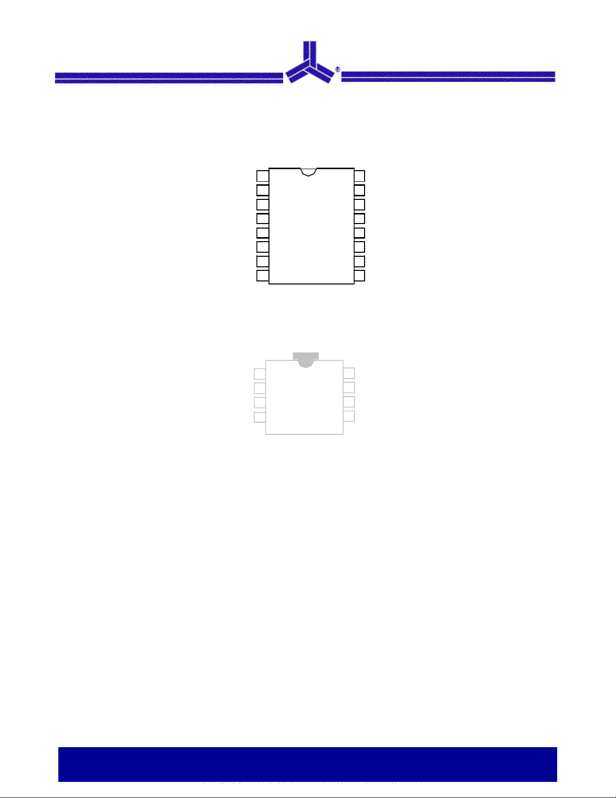
Pin Configuration
V
REF
CLK2
CLK1
GND
1
2
3
4
ASM5P23S09A
5
6
7
8
1
2
ASM5P23S05A
3
4
16
15
14
13
V
12
11
10
9
8
7
CLK4
6
V
DD
CLK3
5
3.3V ‘SpreadTrak’ Zero Delay Buffer 3 of 16
ASM5P23S09A
August 2003 ASM5P23S05A
rev 2.0
Pin Description for ASM5P23S09A
Pin # Pin Name Description
DD
DD
2
Input reference frequency, 5V tolerant input
3
Buffered clock output, bank A
3
Buffered clock output, bank A
3.3V supply
3
Buffered clock output, bank B
3
Buffered clock output, bank B
4
4
Select input, bit 2
Select input, bit 1
3
Buffered clock output, bank B
3
Buffered clock output, bank B
3.3V supply
3
Buffered clock output, bank A
3
Buffered clock output, bank A
1 REF
2 CLKA1
3 CLKA2
4 V
5 GND Ground
6 CLKB1
7 CLKB2
8 S2
9 S1
10 CLKB3
11 CLKB4
12 GND Ground
13 V
14 CLKA3
15 CLKA4
16 CLKOUT3Buffered output, internal feedback on this pin
Pin Description for ASM5P23S05A
Pin # Pin Name Description
1 REF
2 CLK2
3 CLK1
2
Input reference frequency, 5V-tolerant input
3
Buffered clock output
3
Buffered clock output
4 GND Ground
DD
3
Buffered clock output
3.3V supply
3
Buffered clock output
5 CLK3
6 V
7 CLK4
8 CLKOUT 3Buffered clock output, internal feedback on this pin
Notes:
2. Weak pull-down.
3. Weak pull-down on all outputs.
4. Weak pull-up on these inputs.
3.3V ‘SpreadTrak’ Zero Delay Buffer 4 of 16

ASM5P23S09A
August 2003 ASM5P23S05A
rev 2.0
Absolute Maximum Ratings
Parameter Min Max Unit
Supply Voltage to Ground Potential -0.5 +7.0 V
DC Input Voltage (Except REF) -0.5 VDD + 0.5 V
DC Input Voltage (REF) -0.5 7 V
Storage Temperature -65 +150 °C
Max. Soldering Temperature (10 sec) 260 °C
Junction Temperature 150 °C
Static Discharge Voltage
(per MIL-STD-883, Method 3015)
Note: These are stress ratings only and functional usage is not implied. Exposure to absolute maximum
ratings for prolonged periods can affect device reliability.
2000 V
Operating Conditions for ASM5P23S05A and ASM5P23S09A - Commercial Temperature Devices
Parameter Description Min Max Unit
V
DD
T
A
C
C
C
IN
Supply Voltage 3.0 3.6 V
Operating Temperature (Ambient Temperature) 0 70 °C
Load Capacitance, below 100 MHz 30 pF
L
Load Capacitance, from 100 MHz to 133 MHz 10 pF
L
Input Capacitance 7 pF
3.3V ‘SpreadTrak’ Zero Delay Buffer 5 of 16

ASM5P23S09A
/2 on the CLKOUT pins of the device
August 2003 ASM5P23S05A
rev 2.0
Electrical Characteristics for ASM5P23S05A and ASM5P23S09A - Commercial Temperature Devices
Parameter Description Test Conditions Min Max Unit
V
IL
V
IH
I
IL
I
IH
V
OL
V
OH
I
DD
Input LOW Voltage
Input HIGH Voltage
Input LOW Current VIN= 0V 50.0 µA
Input HIGH Current VIN= V
Output LOW Voltage
Output HIGH Voltage
Supply Current Unloaded outputs at 66.67 MHz,
Notes:
5. REF input has a threshold voltage of VDD/2
6. Parameter is guaranteed by design and characterization. Not 100% tested in production
7. S1 / S2 inputs are CMOS, TTL compatible inputs –
The input must toggle somewhere between 0.8 and 2.0. We guarantee the limits of 0.8 and 2.0, but can't guarantee anything tighter than
that. As Vdd moves higher the toggle point will move higher, but will always stay below 2.0V. As Vdd moves lower, the toggle point will
move lower, but always stay higher than 0.8V. What the 2.0V MIN Vih specification means is that you put 2.0V or a higher voltage into the
device, and you will have a logic HIGH. If you put 0.8V or a lower voltage into the device, you will have a logic LOW ( Vil spec = 0.8V max).
It will toggle someplace in between 0.8V and 2.0V, but we don't guarantee exactly where, and the exact point will change depending upon
conditions. Characterization shows we toggle at 1.1V and 1.5V (showing a little hysteresis), everything is perfect. We meet spec, plus have
~ 300mV noise immunity on the low end and ~500mV noise immunity on the high side. Under nominal conditions, with no hysteresis, most
devices will toggle at about 1.5V for both high and low.
Switching Characteristics for ASM5P23S05A-1 and ASM5P23S09A-1 - Commercial Temperature Devices
5
5
DD
6
IOL= 8mA (-1)
2.0 V
0.8 V
100.0 µA
0.4 V
IOH= 12mA (-1H)
6
IOL= -8mA (-1)
2.4 V
IOH= -12mA (-1H)
TBD mA
SEL inputs at V
DD
7
Parameter Description Test Conditions Min Typ Max Unit
1/t
t
LOCK
t
3
t
4
t
5
t
6
t
7
t
J
Output Frequency
1
30-pF load
10-pF load
Duty Cycle 6= (t2 / t1) * 100 Measured at 1.4V, F
Output Rise Time
Output Fall Time
Output-to-output skew
Delay, REF Rising Edge to
CLKOUT Rising Edge
Device-to-Device Skew
Cycle-to-cycle jitter
PLL Lock Time
6
6
6
Measured between 0.8V and 2.0V 2.50 ns
Measured between 2.0V and 0.8V 2.50 ns
All outputs equally loaded 250 ps
Measured at VDD/2 0 ±350 ps
6
6
6
6
Measured at V
Measured at 66.67 MHz, loaded outputs 200 ps
Stable power supply, valid clock presented on
10
10
= 66.67 MHz 40.0 50.0 60.0 %
OUT
DD
100
133.3 3
0 700 ps
1.0 ms
REF pin
Notes:
7. All parameters specified with loaded outputs.
3.3V ‘SpreadTrak’ Zero Delay Buffer 6 of 16
MHz
 Loading...