

Alliance Semiconductor ASM690A, ASM692A, ASM802L, ASM802M, ASM805L Service Manual
查询ASM690A供应商
October 2003
ASM690A / 692A
ASM802L / 802M
ASM805L
rev 1.0
µP Power Supply Supervisor With Battery Backup Switch
General Description
The AS690A / AS692A / AS802L / AS802M / AS805L offers
complete single chip solutions for power supply monitoring and
control battery functions in microprocessor systems. Each
device implements four functions: Reset control, watchdog
monitoring, battery-backup switching and power-failure
monitoring. In addition to microprocessor reset under power-up
and power-down conditions, these devices provide battery-
backup switching to maintain control in power loss and brown-
out situations. Additional monitoring capabilities can provide an
early warning of unregulated power supply loss before the
voltage regulator drops out. The important features of these
four functions are:
• 1.6 second watchdog timer to keep microprocessor
responsive
• 4.40V or 4.65V V
threshold for microprocessor reset at
CC
power-up and power-down
• SPDT (Single-pole, Double-throw) PMOS switch connects
backup power to RAM if V
CC
fails
• 1.25V threshold detector for power loss or general purpose
voltage monitoring
These features are pin-compatible with the industry standard
power-supply supervisors. Short-circuit and thermal protection
have also been added. The AS690A / AS802L / AS805L
generate a reset pulse when the supply voltage drops below
4.65V and the AS692A / AS802M generate a reset below
4.40V. The ASM802L / ASM802M have power-fail accuracy to
± 2%. The ASM805L is the same as the ASM690A except that
RESET is provided instead of RESET
.
Features
• Two precision supply-voltage monitor options
•4.65V (AS690A / AS802L / AS805L)
•4.40V (AS692A / AS802M )
• Battery-backup power switch on-chip
• Watchdog timer: 1.6 second timeout
• Power failure / low battery detection
• Short circuit protection and thermal limiting
• Small 8-pin SO package
• No external components
• Specified over full temperature range
Applications
• Embedded control systems
• Portable/Battery operated systems
• Intelligent instruments
• Wireless instruments
• Wireless communication systems
• PDAs and hand-held equipments
• µP / µC power supply monitoring
• Safety system
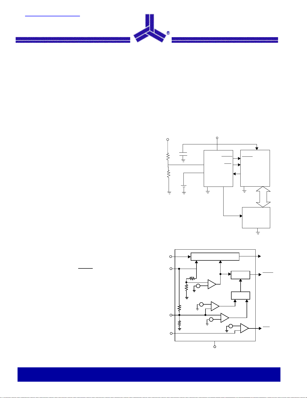
Typical Operating Circuit
Unregulated DC
R
R
0.1 µF
1
2
+
3.6 V
_
Lithium
Battery
PFI
V
BATT
GND
ASM690A
Regulated +5V
V
CC
RESET
PFO
WDI
V
OUT
Block Diagram
8
V
V
BATT
BATT
V
V
WDI
WDI
PFI
PFI
8
2
2
CC
CC
6
6
4
4
ASM690A, ASM692A, ASM802L, ASM802M, (ASM805L)
Battery-Switchover Circuit
Battery-Switchover Circuit
+
+
|+
|+
-
-
1.25V
1.25V
3.5V
3.5V
+
+
|+
|+
-
-
-
-
|+
|+
+
+
0.8V
0.8V
3
GND
Reset
Reset
Generator
Generator
Watchdog
Watchdog
Timer
Timer
1.25V
1.25V
|+
|+
RESET
NMI
I/O LINE
GND
V
CC
GND
-
-
+
+
V
CC
CMOS
RAM
1
1
7
7
5
5
BUS
V
V
OUT
OUT
RESET
RESET
(RESET)
(RESET)
PFO
PFO
Alliance Semiconductor
2575 Augustine Drive . Santa Clara, CA 95054 . Tel: 408.855.4900 . Fax: 408.855.4999 . www.alsc.com
Notice: The information in this document is subject to change without notice
ASM690A / 692A
ASM802L / 802M
October 2003
rev 1.0
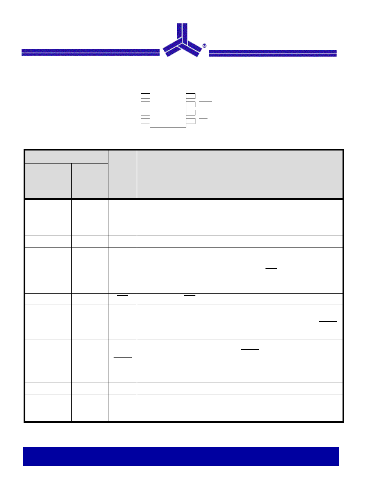
Pin Configuration
Pin Description
Pin Number
ASM690A /
ASM692A
ASM802L /
ASM802M
11
ASM805L
Plastic/CerDip/SO
V
OUT
V
CC
GND
PFI
Name Function
Voltage supply for RAM. When VCC is above the reset threshold, V
V
OUT
V
output will be connected to the backup supply at V
higher) through the MOS switch to provide continuous power to the CMOS RAM.
ASM690A
1
ASM692A
2
ASM802L
3
ASM802M
4
(ASM805L)
through a P-Channel MOS device. If VCC falls below the reset threshold, this
CC
V
8
BATT
7
RESET (RESET)
6
WDI
PFO
5
ASM805L
OUT
(or VCC, whichever is
BATT
connects to
22
3 3 GND Ground
44PFI
55PFO
66WDI
7 - RESET
- 7 RESET Active-HIGH reset output. The inverse of RESET
88
V
CC
V
BATT
+5V power supply input.
Power failure monitor input. PFI is connected to the internal power fail comparator
which is referenced to 1.25V. The power fail output (PFO
remains HIGH if PFI is above 1.25V. If this feature is unused, the PFI pin should be
connected to GND or V
Power-fail output. PFO is active LOW whenever the PFI pin is less than 1.25V.
Watchdog input. The WDI input monitors microprocessor activity. An internal timer
is reset with each transition of the WDI input. If the WDI is held HIGH or LOW for
longer than the watchdog timeout period, typically 1.6 seconds, RESET (or RESET
is asserted for the reset pulse width time, t
Active-LOW reset output. When triggered by VCC falling below the reset threshold
or by watchdog timer timeout, RESET (or RESET
width t
(4.65V in ASM690A / ASM802L and 4.4V in the ASM692A / ASM802L) and
remains low for 200ms after V
Auxiliary power or backup-battery input. V
function is not used. The input has about 40mV of hysteresis to prevent rapid toggling between V
, typically 200ms. It will remain low if VCC is below the reset threshold
RS
and V
CC
OUT
.
, of 140ms, minimum.
RS
rises above the reset threshold.
CC
should be connected to GND if the
BATT
.
BATT
) is active LOW but
)
) pulses low for the reset pulse
.
µP Power Supply Supervisor With Battery Backup Switch
Notice: The information in this document is subject to change without notice
2 of 13

ASM690A / 692A
ASM802L / 802M
October 2003
rev 1.0
Detailed Description
It is important to initialize a microprocessor to a known state
in response to specific events that could create code
execution errors and “lock-up”. The reset output of these
supervisory circuits send a reset pulse to the microprocessor
in response to power-up, power-down/power-loss or a
watchdog time-out.
RESET/RESET
Power-up reset occurs when a rising V
threshold, V
output is asserted in the appropriate logic state for the
duration of t
200ms and is LOW for the ASM690A, ASM692A, ASM802
and HIGH for the ASM805L. Figure 1 shows the reset pin
timing.
Timing
reaches the reset
CC
, forcing a reset condition in which the reset
RT
. The reset pulse width, tRS, is typically around
RS
ASM805L
Application Information
Microprocessor Interface
The ASM690 has logic-LOW RESET output while the
ASM805 has an inverted logic-HIGH RESET output.
Microprocessors with bidirectional reset pins can pose a
problem when the supervisory circuit and the microprocessor
output pins attempt to go to opposite logic states. The
problem can be resolved by placing a 4.7kΩ resistor between
the RESET output and the microprocessor reset pin. This is
shown in Figure 2. Since the series resistor limits drive
capabilities, the reset signal to other devices should be
buffered.
Power-loss or “brown-out” reset occurs when V
the reset threshold resulting in a reset assertion for the
duration of t
V
is between VRT and 1.1V, the lowest VCC for which these
CC
devices can provide a guaranteed logic-low output. To ensure
logic inputs connected to the ASM690A / ASM692A/ASM802
RESET pin are in a known state when V
100kΩ pull-down resistor at RESET is needed: the logic-high
ASM805L will need a pull-up resistor to V
Watchdog Timer
A Watchdog time-out reset occurs when a logic “1” or logic
“0” is continuously applied to the WDI pin for more than 1.6
seconds. After the duration of the reset interval, the watchdog
timer starts a new 1.6 second timing interval; the
microprocessor must service the watchdog input by changing
states or by floating the WDI pin before this interval is
finished. If the WDI pin is held either HIGH or LOW, a reset
pulse will be triggered every 1.8 seconds (the 1.6 second
timing interval plus the reset pulse width t
RS. The reset signal remains asserted as long as
CC
CC
RS
dips below
CC
is under 1.1V, a
.
).
Figure 1: RESET/RESET Timing
V
CC
Power Supply
RESET
ASM690A
GND
Bi-directional I/O pin
4.7K
BUF
V
CC
Ω
RESET
GND
Buffered
RESET
Figure 2: Interfacing with bi-directional
microprocessor reset inputs
µP Power Supply Supervisor With Battery Backup Switch
Notice: The information in this document is subject to change without notice
3 of 13
ASM690A / 692A
ASM802L / 802M
October 2003
rev 1.0
Watchdog Input
As discussed in the Reset section, the Watchdog input is
used to monitor microprocessor activity. It can be used to
insure that the microprocessor is in a continually responsive
state by requiring that the WDI pin be toggled every second.
If the WDI pin is not toggled within the 1.6 second window
(minimum t
the microprocessor to the initial start-up state. Pulses as
short as 50ns can be applied to the WDI pin. If this feature is
not used, the WDI pin should be open circuited or the logic
placed into a high-impedance state to allow the pin to float.
Backup-Battery Switchover
A power loss can be made less severe if the system RAM
contents are preserved. This is achieved in the ASM690/692/
802/805 by switching from the failed V
power source connected at V
reset threshold voltage (V
V
. The V
BATT
2Ω PMOS switch but a brown-out or loss of VCC will cause a
switchover to V
Although both conditions (VCC < VRT and VCC <V
occur for the switchover to V
switched back to V
the voltage at V
device diode (D1 in Figure 3) will be forward biased if V
exceeds VCC by more than a diode drop when VCC is
switched to V
V
be no greater than VRT +0.6V.
BATT
+ tRS), a reset pulse will be asserted to return
WD
to an alternate
CC
when VCC is less than the
BATT
< VRT), and VCC is less than
CC
pin is normally connected to VCC through a
OUT
by means of a 20Ω PMOS switch.
BATT
BATT
to occur, V
BATT
when VCC exceeds VRT irrespective of
CC
. It should be noted that an internal
BATT
. Because of this it is recommended that
OUT
OUT
will be
) must
BATT
ASM805L
V
BATT
D2
SW2
SW1
ASM690A
ASM692A
ASM802L
ASM802M
Figure 3: Internal device configuration of battery
switch-over function
Table 1. Pin Connections in Battery Backup Mode
Pin Connection
V
OUT
V
BATT
PFI Disabled
PFO Logic-LOW
RESET
Connected to V
switch
Connected to V
Logic-LOW (except on ASM805 where it is
HIGH)
D1
ASM805L
D3
V
OUT
through internal PMOS
BATT
OUT
V
SW3
CC
SW4
Condition SW1/SW2 SW3/SW4
V
> Reset Threshold
CC
V
< Reset Threshold
CC
V
> V
CC
BATT
< Reset Threshold
V
CC
V
< V
CC
BATT
ASM690A/802A/805L Reset Threshold = 4.65V
ASM692A /ASM802M Reset Threshold = 4.4V
open closed
open closed
closed open
µP Power Supply Supervisor With Battery Backup Switch
Notice: The information in this document is subject to change without notice
WDI Watchdog timer disabled
During the backup power mode, the internal circuitry of the
supervisory circuit draws power from the battery supply.
While V
and the current drawn by the device is typically 35µA. When
V
CC
switchover comparator, the PFI comparator and WDI
comparator will shut off, reducing the quiescent current drawn
by the IC to less than 1µA.
is still alive, the comparator circuits remain alive
CC
drops more than 1.1V below V
BATT
, the internal
4 of 13
 Loading...