

Alliance Semiconductor ASM5P2309A, ASM5P2305A Service Manual
查询ASM5I2305A-1-08-SR供应商
ASM5P2309A
September 2005 ASM5P2305A
rev 1.6
3.3V Zero Delay Buffer
General Features
15MHz to 133MHz operating range, compatible
with CPU and PCI bus frequencies.
Zero input - output propagation delay.
Multiple low-skew outputs.
Output-output skew less than 250pS.
Device-device skew less than 700pS.
One input drives 9 outputs, grouped as
4 + 4 + 1(ASM5P2309A).
One input drives 5 outputs (ASM5P2305A).
Less than 200 pS cycle-to-cycle jitter is compatible
with Pentium
®
based systems.
Test Mode to bypass PLL (ASM5P2309A only,
Refer Select Input Decoding Table).
Available in 16pin 150-mil SOIC, 4.4 mm TSSOP
(ASM5P2309A), and in 8pin 150-mil SOIC
package (ASM5P2305A).
3.3V operation, advanced 0.35µ CMOS
technology.
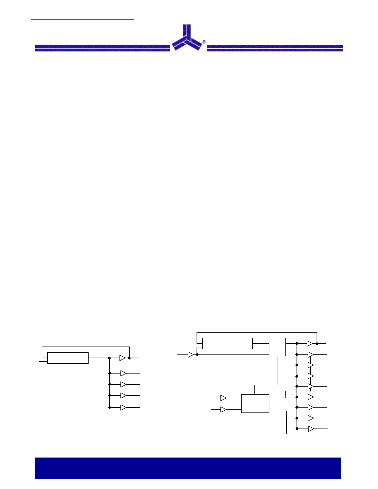
Functional Description
ASM5P2309A is a versatile, 3.3V zero-delay buffer
designed to distribute high-speed clocks. It accepts one
reference input and drives out nine low-skew clocks. It is
available in a 16-pin package. The ASM5P2305A is the
eight-pin version of the ASM5P2309A. It accepts one
reference input and drives out five low-skew clocks.
The -1H version of the ASM5P23XXA operates at up to
Block Diagram
133MHz frequencies, and has higher drive than the -1
devices. All parts have on-chip PLLs that lock to an input
clock on the REF pin. The PLL feedback is on-chip and is
obtained from the CLKOUT pad.
The ASM5P2309A has two banks of four outputs each,
which can be controlled by the Select inputs as shown in
the Select Input Decoding Table. The select input also
allows the input clock to be directly applied to the outputs
for chip and system testing purposes.
Multiple ASM5P2309A and ASM5P2305A devices can
accept the same input clock and distribute it. In this case
the skew between the outputs of the two devices is
guaranteed to be less than 700pS.
All outputs have less than 200pS of cycle-to-cycle jitter.
The input and output propagation delay is guaranteed to be
less than 350pS, and the output to output skew is
guaranteed to be less than 250pS.
The ASM5P2309A and the ASM5P2305A are available in
two different configurations, as shown in the ordering
information table. The ASM5P2305A-1/ ASM5P2309A-1 is
the base part. The ASM5P2305A-1H/ ASM5P2309A-1H is
the high drive version of the -1 and its rise and fall times
are much faster than -1 part.
REF
PLL
ASM5P2305A
CLKOUT
CLK1
CLK2
CLK3
CLK4
REF
S2
S1
PLL
ASM5P2309A
MUX
Select Input
Decoding
CLKOUT
CLKA1
CLKA2
CLKA3
CLKA4
CLKB1
CLKB2
CLKB3
CLKB4
Alliance Semiconductor
2575 Augustine Drive • Santa Clara, CA • Tel: 408.855.4900 • Fax: 408.855.4999 • www.alsc.com
Notice: The information in this document is subject to change without notice.
ASM5P2309A
September 2005
ASM5P2305A
rev 1.6
Select Input Decoding for ASM5P2309A
S2 S1 Clock A1 - A4 Clock B1 - B4 CLKOUT1 Output Source
0 0 Three-state Three-state Driven PLL N
0 1 Driven Three-state Driven PLL N
1 0 Driven Driven Driven Reference Y
1 1 Driven Driven Driven PLL N
Notes:
1. This output is driven and has an internal feedback for the PLL. The load on this output can be adjusted to change the skew between the reference and the
output.
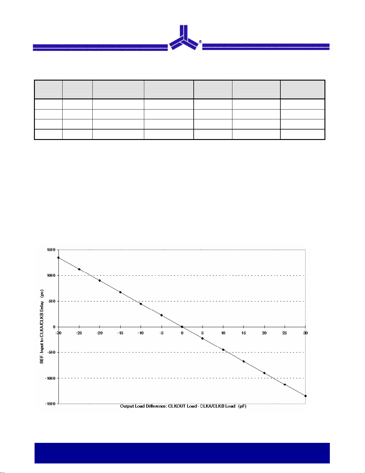
Zero Delay and Skew Control
All outputs should be uniformly loaded to achieve Zero
Delay between input and output. Since the CLKOUT pin is
the internal feedback to the PLL, its relative loading can
adjust the input-output delay.
For applications requiring zero input-output delay, all
outputs, including CLKOUT, must be equally loaded. Even
if CLKOUT is not used, it must have a capacitive load equal
to that on other outputs, for obtaining zero-input-output
delay.
PLL
Shut-Down
Notice: The information in this document is subject to change without notice.
3.3V Zero Delay Buffer 2 of 20

ASM5P2309A
September 2005
ASM5P2305A
rev 1.6
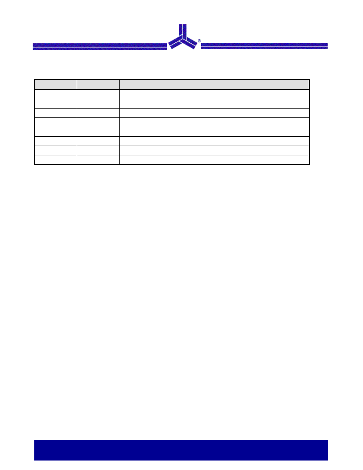
Pin Configuration
REF
CLKA1
CLKA2
V
DD
GND
CLKB1
CLKB2
S2
1
2
3
4
ASM5P2309A
5
6
7
8
REF
1
2
CLK2
CLK1
GND
ASM5P2305A
3
4
Pin Description for ASM5P2309A
Pin # Pin Name Description
1 REF2 Input reference frequency, 5V tolerant input
2 CLKA13 Buffered clock output, bank A
3 CLKA23 Buffered clock output, bank A
4 VDD 3.3V supply
5 GND Ground
6 CLKB13 Buffered clock output, bank B
7 CLKB23 Buffered clock output, bank B
8 S24 Select input, bit 2
9 S14 Select input, bit 1
10 CLKB33 Buffered clock output, bank B
11 CLKB43 Buffered clock output, bank B
12 GND Ground
13 VDD 3.3V supply
14 CLKA33 Buffered clock output, bank A
15 CLKA43 Buffered clock output, bank A
16 CLKOUT3 Buffered output, internal feedback on this pin
8
7
6
5
CLKOUT
16
15
CLKA4
14
CLKA3
13
V
DD
12
GND
CLKB4
11
CLKB3
10
S1
9
CLKOUT
CLK4
V
DD
CLK3
3.3V Zero Delay Buffer 3 of 20
Notice: The information in this document is subject to change without notice.
ASM5P2309A
September 2005
ASM5P2305A
rev 1.6
Pin Description for ASM5P2305A
Pin # Pin Name Description
1 REF2 Input reference frequency, 5V-tolerant input
2 CLK2
3 CLK13 Buffered clock output
4 GND Ground
5 CLK3
6 VDD 3.3V supply
7 CLK43 Buffered clock output
8 CLKOUT
Notes:
2. Weak pull-down.
3. Weak pull-down on all outputs.
4. Weak pull-up on these inputs.
3
Buffered clock output
3
Buffered clock output
3
Buffered clock output, internal feedback on this pin
3.3V Zero Delay Buffer 4 of 20
Notice: The information in this document is subject to change without notice.

ASM5P2309A
September 2005
ASM5P2305A
rev 1.6
Absolute Maximum Ratings
Parameter Min Max Unit
Supply Voltage to Ground Potential -0.5 +7.0 V
DC Input Voltage (Except REF) -0.5 VDD + 0.5 V
DC Input Voltage (REF) -0.5 7 V
Storage Temperature -65 +150 °C
Max. Soldering Temperature (10 sec) 260 °C
Junction Temperature 150 °C
Static Discharge Voltage
(As per JEDEC STD22- A114-B)
Note: These are stress ratings only and functional usage is not implied. Exposure to absolute maximum ratings for prolonged periods can
affect device reliability.
Operating Conditions for ASM5P2305A and ASM5P2309A - Commercial Temperature Devices
Parameter Description Min Max Unit
VDD Supply Voltage 3.0 3.6 V
TA Operating Temperature (Ambient Temperature) 0 70 °C
CL Load Capacitance, below 100MHz 30 pF
CL Load Capacitance, from 100MHz to 133MHz 10 pF
CIN Input Capacitance 7 pF
2000
V
3.3V Zero Delay Buffer 5 of 20
Notice: The information in this document is subject to change without notice.
ASM5P2309A
September 2005
ASM5P2305A
rev 1.6
Electrical Characteristics for ASM5P2305A and ASM5P2309A - Commercial Temperature Devices
Parameter Description Test Conditions Min Typ Max Unit
VIL Input LOW Voltage 5 0.8 V
VIH Input HIGH Voltage 5 2.0 V
IIL Input LOW Current VIN = 0V 50 µA
IIH Input HIGH Current VIN = VDD 100 µA
VOL
VOH
IDD
Output LOW Voltage
Output HIGH Voltage
Supply Current
6
6
Zo Output Impedance 23 Ω
Switching Characteristics for ASM5P2305A-1 and ASM5P2309A-1 -- Commercial Temperature Devices7
= 8mA (-1)
I
OL
= 12mA (-1H)
I
OH
= -8mA (-1)
I
OL
= -12mA (-1H)
I
OH
Unloaded outputs at 66.67MHz,
SEL inputs at V
DD
0.4 V
2.4 V
34 mA
Parameter Description Test Conditions Min Typ Max Unit
1/t1 Output Frequency
Duty Cycle6 = (t2 / t1) * 100 Measured at 1.4V, F
30pF load
10pF load
= 66.67MHz 40 50 60 %
OUT
t3 Output Rise Time6 Measured between 0.8V and 2.0V 2.50 nS
t4 Output Fall Time 6 Measured between 2.0V and 0.8V 2.50 nS
t5 Output-to-output skew
t6
Delay, REF Rising Edge to
CLKOUT Rising Edge
t7 Device-to-Device Skew
tJ Cycle-to-cycle jitter
t
PLL Lock Time 6
LOCK
Notes:
5. REF input has a threshold voltage of V
6. Parameter is guaranteed by design and characterization. Not 100% tested in production
7. All parameters specified with loaded outputs.
6
All outputs equally loaded 250 pS
Measured at V
6
Measured at V
6
of the device
6
Measured at 66.67MHz, loaded outputs 200 pS
/2 0 ±350 pS
DD
/2 on the CLKOUT pins
DD
Stable power supply, valid clock
presented on REF pin
/2
DD
15
15
100
133
MHz
0 700 pS
1.0 mS
3.3V Zero Delay Buffer 6 of 20
Notice: The information in this document is subject to change without notice.
 Loading...