

Alliance Semiconductor ASM5I9773A Service Manual

查询ASM5I9773A供应商
June 2005 ASM5I9773A
rev 0.3
2.5V or 3.3V, 200-MHz, 12-Output Zero Delay Buffer
Features
Output frequency range: 8.33MHz to 200MHz
Input frequency range: 6.25MHz to 125MHz
2.5V or 3.3V operation
Split 2.5V / 3.3V outputs
±2%( max ) Output duty cycle variation
12 Clock outputs: drive up to 24 clock lines
One feedback output
Three reference clock inputs: LVPECL or LVCMOS
300pS ( max ) output-output skew
The ASM5I9773A features one LVPECL and two LVCMOS
reference clock inputs and provides 12 outputs partitioned
in three banks of four outputs each. Each bank divides the
VCO output per SEL(A:C) settings (see Table 2. Function
Table (Configuration Controls)). These dividers allow
output-to-input ratios of 8:1, 6:1, 5:1, 4:1, 3:1, 8:3, 5:2, 2:1,
5:3, 3:2, 4:3, 5:4, 1:1, and 5:6. Each LVCMOS-compatible
output can drive 50Ω series- or parallel-terminated
transmission lines. For series-terminated transmission
lines, each output can drive one or two traces, giving the
device an effective fanout of 1:24.
Phase-locked loop (PLL) bypass mode
‘SpreadTrak’
Output enable/disable
Pin-compatible with CY29773, MPC9773 and
MPC973
Industrial temperature range: –40°C to +85°C
52pin 1.0mm TQFP package
RoHS Compliance
Functional Description
The ASM5I9773A is a low-voltage high-performance
200-MHz PLL-based zero delay buffer designed for high
speed clock distribution applications.
The PLL is ensured stable, given that the VCO is
configured to run between 200 MHz to 500 MHz. This
allows a wide range of output frequencies, from 8 MHz to
200 MHz. For normal operation, the external feedback
input FB_IN is connected to the feedback output FB_OUT.
The internal VCO is running at multiples of the input
reference clock set by the feedback divider (see Table 1.
Frequency Table).
When PLL_EN is LOW, PLL is bypassed and the reference
clock directly feeds the output dividers. This mode is fully
static and the minimum input clock frequency specification
does not apply.
Alliance Semiconductor
2575, Augustine Drive • Santa Clara, CA • Tel: 408.855.4900 • Fax: 408.855.4999 • www.alsc.com
Notice: The information in this document is subject to change without notice.
K
K
K
K
June 2005
ASM5I9773A
rev 0. 3
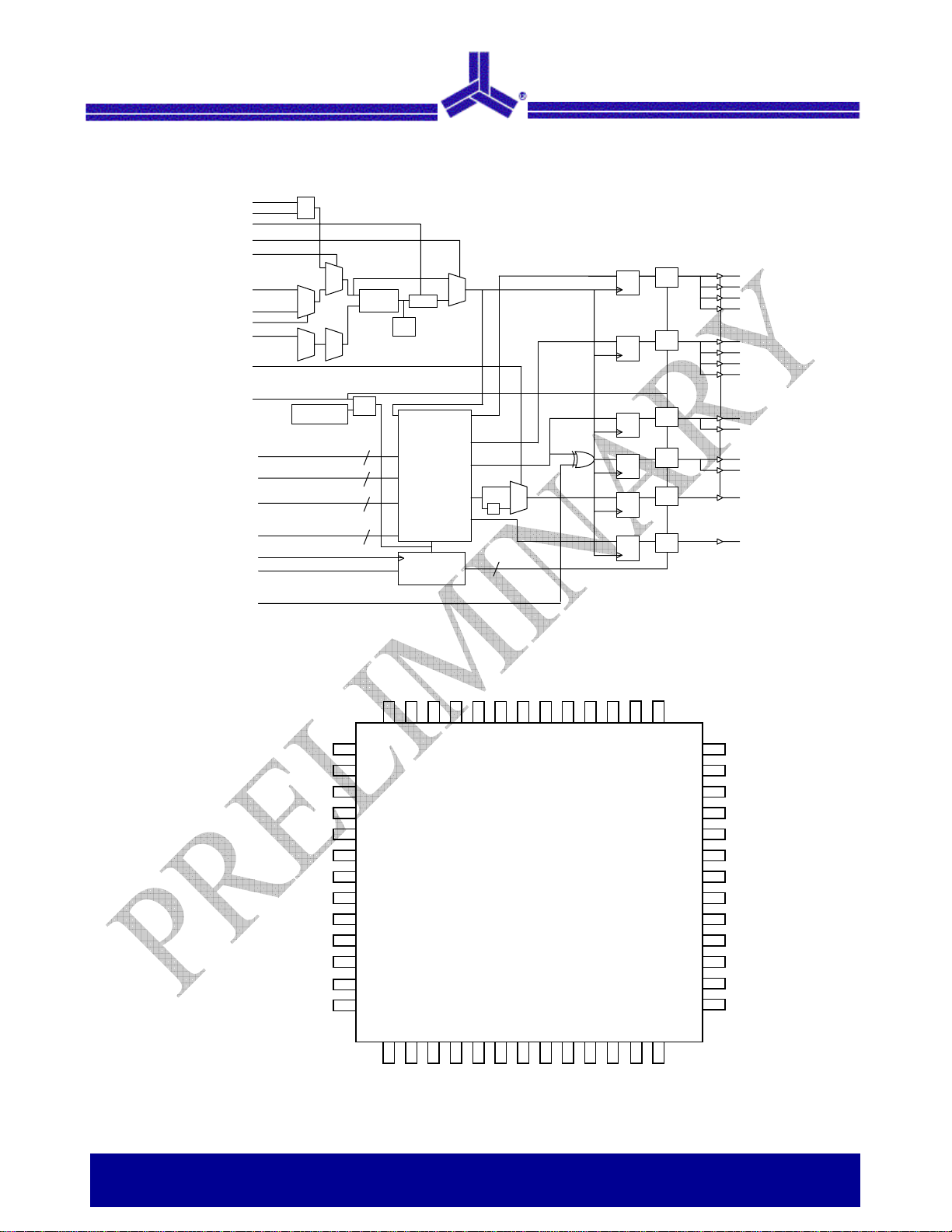
Block Diagram
Pin Configuration
PECL_CL
PECL_CLK#
VCO_SEL
TCLK_SEL
FB_SEL(0,1)
PLL_EN
REF_SEL
TCLK0
TCLK1
FB_IN
FB_SEL2
MR#/OE
SELA(0,1)
SELB(0,1)
SELC(0,1)
SCL
SDATA
INV_CL
0
1
Power-On
Reset
2
2
2
2
Phase
Detector
VCO
LPF
/2,/4,/6,/8
Data Generator
Output Disable
Circuitry
VCO_SEL
VSS
0
1
/4,/6,/8,/12
/4,/6,/8,/10
/4,/6,/8,/10
Sync Pulse
QA0
/2
12
VDDQA
QA1
0
1
VSS
QA2
QA3
VDDQA
D QD Q
D Q
D Q
D Q
D Q
D Q
SELA1
SELA0
Sync
Frz
Sync
Frz
Sync
Frz
Sync
Frz
Sync
Frz
Sync
Frz
SELB1
SELB0
QA0
QA1
QA2
QA3
QB0
QB1
QB2
QB3
QC0
QC1
QC2
QC3
FB_OUT
SYNC
AVSS
MR#/OE
SCLK
SDATA
FB_SEL2
PLL_EN
REF_SEL
TCLK_SEL
TCLK0
TCLK1
PECL_CLK
PECL_CLK#
AVDD
52 51 50 49
1
2
3
4
5
6
7
8
9
10
11
12
13
14 15 16 17
VSS
INV_CL
48
47 46
ASM5I9773A
18
19 20
QC2
QC3
VDDQC
SELC1
SELC0
43
45
44 41 40
42
21
22 23 24
QC1
VDDQC
QC0
25
VSS
26
SYNC
39
38
37
36
35
34
33
32
31
30
29
28
27
FB_SEL1
VSS
QB0
VDDQB
QB1
VSS
QB2
VDDQB
QB3
FB_IN
VSS
FB_OUT
VDD
FB_SEL0
2.5V or 3.3V, 200 MHz, 12-Output Zero Delay Buffer 2 of 16
Notice: The information in this document is subject to change without notice.
June 2005
ASM5I9773A
rev 0. 3
Pin Configuration
Pin Name I/O Type Description
11 PECL_CLK I, PU LVPECL
12 PECL_CLK# I LVPECL
9 TCLK0 I, PU LVCMOS
10 TCLK1 I, PU LVCMOS
44,46,48,50 QA(3:0) O LVCMOS
32,34,36,38 QB(3:0) O LVCMOS
16,18,21,23 QC(3:0) O LVCMOS
29 FB_OUT O LVCMOS
31 FB_IN I, PU LVCMOS
25 SYNC O LVCMOS
6 PLL_EN I, PU LVCMOS
2 MR#/OE I, PU LVCMOS
8 TCLK_SEL I, PU LVCMOS
7 REF_SEL I, PU LVCMOS
52 VCO_SEL I, PU LVCMOS
14 INV_CLK I, PU LVCMOS
5,26,27 FB_SEL(2:0) I, PU LVCMOS
42,43 SELA(1,0) I, PU LVCMOS
40,41 SELB(1,0) I, PU LVCMOS
19,20 SELC(1,0) I, PU LVCMOS
3 SCLK I, PU LVCMOS
4 SDATA I, PU LVCMOS
45,49 VDDQA Supply VDD
33,37 VDDQB Supply VDD
22,17 VDDQC Supply VDD
13 AVDD Supply VDD
28 VDD Supply VDD
1 AVSS Supply Ground
15,24,30,35,
39,47,51
Notes:
1. PU = Internal pull up, PD = Internal pull down.
2. A 0.1µF bypass capacitor should be placed as close as possible to each positive power pin (<0.2”). If these bypass capacitors are not close to the pins their
high frequency filtering characteristics will be cancelled by the lead inductance of the traces.
3. AVDD and VDD pins must be connected to a power supply level that is at least equal or higher than that of VDDQA, VDDQB, and VDDQC power supply pins.
1
LVPECL reference clock input.
LVPECL reference clock input.
LVCMOS/LVTTL reference clock input.
LVCMOS/LVTTL reference clock input.
Clock output bank A.
Clock output bank B.
Clock output bank C.
Feedback clock output. Connect to FB_IN for normal operation.
Feedback clock input. Connect to FB_OUT for normal operation. This
input should be at the same voltage rail as input reference clock.
See Table 1. Frequency Table.
Synchronous pulse output. This output is used for system
synchronization.
PLL enable/bypass input. When Low, PLL is disabled/bypassed and
the input clock connects to the output dividers.
Master reset and Output enable/disable input.
See Table 2. Function Table (Configuration Controls).
LVCMOS Clock reference select input.
See Table 2. Function Table (Configuration Controls).
LVCMOS/LVPECL Reference select input.
See Table 2. Function Table (Configuration Controls).
VCO Operating frequency select input.
See Table 2. Function Table (Configuration Controls).
QC(2,3) Phase selection input.
See Table 2. Function Table (Configuration Controls).
Feedback divider select input. See Table 6.
Frequency select input, Bank A.
See Table 3. Function Table (Bank A).
Frequency select input, Bank B.
See Table 4. Function Table (Bank B).
Frequency select input, Bank C.
See Table 5. Function Table (Bank C).
Serial clock input.
Serial data input.
2.5V or 3.3V Power supply for bank A output clocks
2.5V or 3.3V Power supply for bank B output clocks
2.5V or 3.3V Power supply for bank C output clocks
2.5V or 3.3V Power supply for PLL
2.5V or 3.3V Power supply for core and inputs
Analog Ground.
VSS Supply Ground
Common Ground.
2,3
2,3
.
2,3
.
2,3
.
.
2,3
.
2.5V or 3.3V, 200 MHz, 12-Output Zero Delay Buffer 3 of 16
Notice: The information in this document is subject to change without notice.
June 2005
ASM5I9773A
rev 0. 3
‘SpreadTrak’
Many systems being designed now utilize a technology
called Spread Spectrum Frequency Timing Generation.
ASM5I9773A is designed so as not to filter off the Spread
Spectrum feature of the Reference Input, assuming it
exists.
Table 1: Frequency Table
Feedback
Output Divider
÷4 Input Clock * 4 50 MHz to 125 MHz 50 MHz to 95 MHz
÷6 Input Clock * 6 33.3 MHz to 83.3 MHz 33.3 MHz to 63.3 MHz
÷8. Input Clock * 8 25 MHz to 62.5 MHz 25 MHz to 47.5 MHz
÷10 Input Clock * 10 20 MHz to 50 MHz 20 MHz to 38 MHz
÷12 Input Clock * 12 16.6 MHz to 41.6 MHz 16.6 MHz to 31.6 MHz
÷16 Input Clock * 16 12.5 MHz to 31.25 MHz 12.5 MHz to 23.75 MHz
÷20 Input Clock * 20 10 MHz to 25 MHz 10 MHz to19 MHz
÷24 Input Clock * 24 8.3 MHz to 20.8 MHz 8.3 MHz to 15.8 MHz
÷32 Input Clock * 32 6.25 MHz to 15.625 MHz 6.25 MHz to 11.8 MHz
÷40 Input Clock * 40 5 MHz to 12.5 MHz 5 MHz to 9.5 MHz
VCO
Input Frequency Range
Table 2. Function Table (Configuration Controls)
Control Default 0 1
REF_SEL 1 TCLK0, TCLK1 PECL_CLK
TCLK_SEL 1 TCLK0 TCLK1
VCO_SEL 1 VCO÷2 (low input frequency range)
PLL_EN 1
INV_CLK 1 QC2 and QC3 are in phase with QC0 and QC1
MR#/OE 1
Bypass mode, PLL disabled. The input clock connects to
the output dividers
Outputs disabled (three-state) and reset of the device.
During reset/output disable the PLL feedback loop is open
and the VCO running at its minimum frequency. The device
is reset by the internal power-on reset (POR) circuitry
during power-up.
When a zero delay buffer is not designed to pass the
Spread Spectrum feature through, the result is a
significant amount of tracking skew which may cause
problems in the systems requiring synchronization.
Input Frequency Range
(AVDD = 3.3V)
VCO÷1
(high input frequency range)
PLL enabled. The VCO output
connects to the output dividers
QC2 and QC3 are inverted
(180° phase shift) with respect to
QC0 and QC1
Outputs enabled
(AVDD = 2.5V)
2.5V or 3.3V, 200 MHz, 12-Output Zero Delay Buffer 4 of 16
Notice: The information in this document is subject to change without notice.
June 2005
ASM5I9773A
rev 0. 3
Table 3. Function Table (Bank A)
VCO_SEL SELA1 SELA0 QA(0:3)
0 0 0 ÷8
0 0 1 ÷12
0 1 0 ÷16
0 1 1 ÷24
1 0 0 ÷4
1 0 1 ÷6
1 1 0 ÷8
1 1 1 ÷12
Table 4. Function Table (Bank B)
VCO_SEL SELB1 SELB0 QB(0:3)
0 0 0 ÷8
0 0 1 ÷12
0 1 0 ÷16
0 1 1 ÷20
1 0 0 ÷4
1 0 1 ÷6
1 1 0 ÷8
1 1 1 ÷10
Table 5. Function Table (Bank C)
VCO_SEL SELC1 SELC0 QC(0:3)
0 0 0 ÷4
0 0 1 ÷8
0 1 0 ÷12
0 1 1 ÷16
1 0 0 ÷2
1 0 1 ÷4
1 1 0 ÷6
1 1 1 ÷8
Table 6. Function Table (FB_OUT)
VCO_SEL FB_SEL2 FB_SEL1 FB_SEL0 FB_OUT
0 0 0 0 ÷8
0 0 0 1 ÷12
0 0 1 0 ÷16
0 0 1 1 ÷20
0 1 0 0 ÷16
0 1 0 1 ÷24
0 1 1 0 ÷32
0 1 1 1 ÷40
1 0 0 0 ÷4
1 0 0 1 ÷6
1 0 1 0 ÷8
1 0 1 1 ÷10
1 1 0 0 ÷8
1 1 0 1 ÷12
1 1 1 0 ÷16
1 1 1 1 ÷20
Absolute Maximum Conditions
Parameter Description Condition Min Max Unit
VDD DC Supply Voltage –0.3 5.5 V
VDD DC Operating Voltage Functional 2.375 3.465 V
VIN DC Input Voltage Relative to VSS –0.3 VDD+ 0.3 V
V
DC Output Voltage Relative to VSS –0.3 VDD+ 0.3 V
OUT
VTT Output termination Voltage VDD ÷2 V
LU Latch-up Immunity Functional 200 - mA
RPS Power Supply Ripple Ripple Frequency < 100 kHz 150 mVp-p
TS Temperature, Storage Non-functional –65 +150 °C
TA Temperature, Operating Ambient Functional –40 +85 °C
TJ Temperature, Junction Functional +150 °C
ØJC Dissipation, Junction to Case Functional 23 °C/W
ØJA Dissipation, Junction to Ambient Functional 55 °C/W
ESDH ESD Protection (Human Body Model) 2000 V
FIT Failure in Time Manufacturing test 10 ppm
Note: These are stress ratings only and are not implied for functional use. Exposure to absolute maximum ratings for prolonged periods of time may affect
device reliability.
2.5V or 3.3V, 200 MHz, 12-Output Zero Delay Buffer 5 of 16
Notice: The information in this document is subject to change without notice.
 Loading...