

Alliance Semiconductor ASM5I961P Service Manual
Q
Q1Q2Q
July 2005 ASM5I961P
rev 0.2
Low Voltage Zero Delay Buffer
Features
Fully Integrated PLL
reference clock while the ASM5I961P offers an LVPECL
reference clock.
Up to 200MHz I/O Frequency
LVCMOS Outputs
Outputs Disable in High Impedance
LVPECL Reference Clock Options
LQFP Packaging
±50pS Cycle–Cycle Jitter
150pS Output Skews
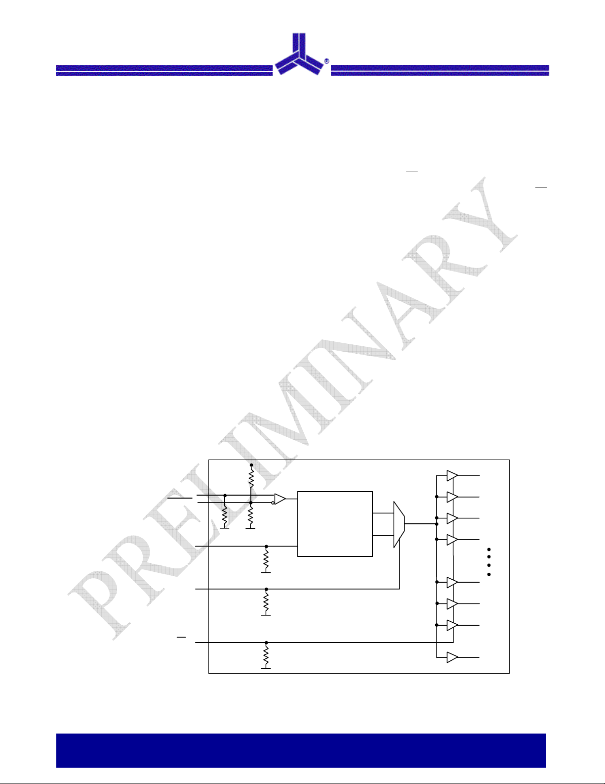
Functional Description
The ASM5I961P is a 2.5V or 3.3V compatible, 1:18 PLL
based zero delay buffer. With output frequencies of up to
200MHz, output skews of 150pS the device meets the
needs of the most demanding clock tree applications.
The ASM5I961P is offered with two different input
configurations. The ASM5I961P offers an LVCMOS
Block Diagram
V
CC
50K
PCLK
PCLK
50K
50K
FB_IN
50K
F_RANGE
50K
OE
50K
Figure 1. ASM5I961P Logic Diagram
When pulled high the OE pin will force all of the outputs
(except QFB) into a high impedance state. Because the OE
pin does not affect the QFB output, down stream clocks
can be disabled without the internal PLL losing lock.
The ASM5I961P is fully 2.5V or 3.3V compatible and
requires no external loop filter components. All control
inputs accept LVCMOS compatible levels and the outputs
provide low impedance LVCMOS outputs capable of
driving terminated 50 transmission lines. For series
terminated lines the ASM5I961P can drive two lines per
output giving the device an effective fanout of 1:36. The
device is packaged in a 32 lead LQFP package to provide
the optimum combination of board density and
performance.
Ref
PLL
100-200 MHz
50-100 MHz
FB
0
1
0
3
Q14
Q15
Q16
QFB
Alliance Semiconductor
2575 Augustine Drive • Santa Clara, CA • Tel: 408.855.4900 • Fax: 408.855.4999 • www.alsc.com
Notice: The information in this document is subject to change without notice.

K
K
July 2005
ASM5I961P
rev 0.2
Pin Configuration
Q5
Q4
Q3
GND
Q2
Q1
Q0
VCC
VCC
Q6
Q7
Q8
GND
24 23 22 21
25
26
27
28
29
30
31
32
ASM5I961P
ASM5I961C
1 2 3 4 5 6 7
20
Q9
Q10
19 18
17
8
Q11
16
15
14
13
12
11
10
VCC
Q12
Q13
Q14
GND
Q15
Q16
9
QFB
Table 1: Pin Configuration
Pin #
2,3
7 FB_IN Input LVCMOS
4 F_RANGE Input LVCMOS PLL frequency range select
6
31,30,29,27,26,25,23,22,21
,19,18,17,15,14,13,11,10
9 QFB Output LVCMOS
1,12,20,28 GND Supply Power Negative power supply
5 VCCA Supply Power
8,16,24,32 VCC Supply Power Positive power supply for I/O and core
GND
PCL
PCL
VCCAOEFB_IN
F_RANGE
VCC
Figure 2. ASM5I961P 32-Lead Package Pinout (Top View)
Pin Name I/O Type Function
¯¯¯¯¯
PCLK, PCLK
OE¯¯
Q0 - Q16 Output LVCMOS Clock outputs
Input LVCMOS PLL reference clock signal
PLL feedback signal input, connect to a QFB
output
Input LVCMOS Output enable/disable
PLL feedback signal output, connect to a
FB_IN
PLL positive power supply (analog power
supply). The ASM5I961P requires an
external RC filter for the analog power
supply pin VCCA. Please see applications
section for details.
Low Voltage Zero Delay Buffer 2 of 14
Notice: The information in this document is subject to change without notice.
July 2005
ASM5I961P
rev 0.2
Table 2: Function Table
Control Default 0 1
PLL high frequency range. ASM5I961P input
F_RANGE 0
reference and output clock frequency range is
100 – 200 MHz
OE¯¯
0 Outputs enabled Outputs disabled (high–impedance state)
Table 3: Absolute Maximum Ratings
Symbol Parameter Min Max Unit
VCC Supply Voltage –0.3 3.6 V
VIN DC Input Voltage –0.3 VCC + 0.3 V
V
DC Output Voltage –0.3 VCC + 0.3 V
OUT
IIN DC Input Current ±20 mA
I
DC Output Current ±50 mA
OUT
TS Storage Temperature Range –40 125 °C
TDV
Note: These are stress ratings only and are not implied for functional use. Exposure to absolute maximum ratings for prolonged periods of time may affect
device reliability.
Static Discharge Voltage
(As per JEDEC STD 22- A114-B)
Table 4: DC Characteristics
(VCC = 3.3V ± 5%, TA = -40°C to +85°C)
Symbol Characteristic Min Typ Max Unit Condition
VIH Input HIGH Voltage 2.0 VCC + 0.3 V LVCMOS
VIL Input LOW Voltage –0.3 0.8 V LVCMOS
VPP
V
CMR
Peak–to–peak input voltage
PECL_CLK, PECL_CLK
Common Mode Range
PECL_CLK, PECL_CLK
1
¯¯¯¯¯¯¯¯¯¯
1
¯¯¯¯¯¯¯¯¯¯
500 1000 mV LVPECL
1.2 V
VOH Output HIGH Voltage 2.4 V IOH = –20mA2
VOL Output LOW Voltage 0.55 V I
Z
Output Impedance 14 20
OUT
IIN Input Current ±120 mA
CIN Input Capacitance 4.0 pF
CPD Power Dissipation Capacitance 8.0 10 pF Per Output
I
Maximum PLL Supply Current 2.0 5.0 mA V
CCA
ICC Maximum Quiescent Supply Current mA All VCC Pins
VTT Output Termination Voltage VCC÷2 V
Notes:
1. Exceeding the specified V
2. The ASM5I961P is capable of driving 50Ω transmission lines on the incident edge. Each output drives one 50Ω parallel terminated transmission line to a
termination voltage of V
window results in a tPD changes of approx. 250pS.
CMR/VPP
. Alternatively, the device drives up two 50Ω series terminated transmission lines.
TT
PLL low frequency range. ASM5I961P input
reference and output clock frequency range is
50 – 100 MHz
2 KV
– 0.8 V LVPECL
CC
= 20mA2
OL
Pin
CCA
Low Voltage Zero Delay Buffer 3 of 14
Notice: The information in this document is subject to change without notice.
July 2005
ASM5I961P
rev 0.2
Table 5: AC Characteristics (V
= 3.3V ± 5%, TA = -40°C to +85°C)
CC
Symbol Characteristic Min Typ Max Unit Condition
f
Input Frequency
ref
f
max
f
Reference Input Duty Cycle 25 75 %
refDC
t
(φ)
t
sk(O)
Maximum Output
Frequency
Propagation Delay
(static phase offset)
Output to Output Skew
DCO Output Duty Cycle
tr, tf Output Rise/Fall Time 0.1 1.0 nS 0.55 to 2.4V
t
Output Disable Time 10 nS
PLZ,HZ
t
Output Enable Time 10 nS
PZL,LZ
t
Cycle to Cycle Jitter
JIT(CC)
t
Period Jitter
JIT(PER)
t
JIT(φ)
t
Maximum PLL Lock Time 10 mS
lock
Notes:
1. AC characteristics apply for parallel output termination of 50 to V
applies for V
2. t
PD
3. See applications section for part to part skew calculation
4. See applications section for calculation for other confidence factors than 1σ
I/O Phase Jitter
= VCC–1.3V and VPP = 800mV
CMR
Table 6: DC Characteristics (V
F_RANGE = 0
F_RANGE = 1
F_RANGE = 0
F_RANGE = 1
2
PECL_CLK to
FB_IN
3
F_RANGE = 0
F_RANGE = 1
RMS (1σ)
4
RMS (1σ)
RMS (1σ)
F_RANGE = 0
F_RANGE = 1
= 2.5V ± 5%, TA = –40° to 85°C)
CC
.
TT
Symbol Characteristic Min Typ Max Unit Condition
VIH Input HIGH Voltage
VIL Input LOW Voltage
VPP
V
CMR
Peak–to–peak input voltage
PECL_CLK, PECL_CLK
Common Mode Range
PECL_CLK, PECL_CLK
1
¯¯¯¯¯¯¯¯¯¯
1
¯¯¯¯¯¯¯¯¯¯
VOH Output HIGH Voltage
VOL Output LOW Voltage
Z
Output Impedance
OUT
IIN Input Current ±120 mA
CIN Input Capacitance 4.0 pF
CPD Power Dissipation Capacitance 8.0 10 pF Per Output
I
Maximum PLL Supply Current 2.0 5.0 mA V
CCA
ICC Maximum Quiescent Supply Current mA All VCC Pins
VTT Output Termination Voltage VCC÷2 V
Notes:
1. Exceeding the specified V
2. The ASM5I961P is capable of driving 50Ω transmission lines on the incident edge. Each output drives one 50Ω parallel terminated transmission line to a
termination voltage of V
window results in a tPD changes of < 250 pS.
CMR/VPP
. Alternatively, the device drives up two 50Ω series terminated transmission lines.
TT
1.7
–0.3
500
1.2
1.8
1
100
50
100
50
200
100
200
100
MHz
MHz
–50 225 pS PLL locked
90 150 pS
42
45
50
50
55
55
%
15 pS
7.0 10 pS
T = Clock
0.0015 ⋅ T
0.0010 ⋅ T
nS
Signal
Period
VCC + 0.3 V LVCMOS
0.7 V LVCMOS
1000 mV LVPECL
V
– 0.7 V LVPECL
CC
V IOH = –15mA2
0.6 V I
= 15mA2
OL
18 26
CCA
Pin
Low Voltage Zero Delay Buffer 4 of 14
Notice: The information in this document is subject to change without notice.
July 2005
ASM5I961P
rev 0.2
Table 7: AC Characteristics (V
= 2.5V ± 5%, TA = -40°C to +85°C)
CC
Symbol Characteristic Min Typ Max Unit Condition
2
3
F_RANGE = 0
F_RANGE = 1
F_RANGE = 0
F_RANGE = 1
PECL_CLK to
FB_IN
F_RANGE = 0
F_RANGE = 1
RMS (1σ)
4
RMS (1σ)
RMS (1σ)
F_RANGE = 0
F_RANGE = 1
.
TT
f
Input Frequency
ref
f
max
f
Reference Input Duty Cycle 25 75 %
refDC
t
(φ)
t
sk(O)
Maximum Output
Frequency
Propagation Delay
(static phase offset)
Output–to–Output Skew
DCO Output Duty Cycle
tr, tf Output Rise/Fall Time 0.1 1.0 nS 0.6 to 1.8V
t
Output Disable Time 10 nS
PLZ,HZ
t
Output Enable Time 10 nS
PZL,LZ
t
Cycle–to–Cycle Jitter
JIT(CC)
t
Period Jitter
JIT(PER)
t
JIT(φ)
t
Maximum PLL Lock Time 10 mS
lock
Notes:
1. AC characteristics apply for parallel output termination of 50 to V
applies for V
2. t
PD
3. See applications section for part–to–part skew calculation
4. See applications section for calculation for other confidence factors than 1σ
I/O Phase Jitter
= VCC–1.3V and VPP = 800mV
CMR
1
100
50
100
50
200
100
200
100
MHz
MHz
–50 175 pS PLL locked
90 150 pS
40
45
50
50
60
55
%
15 pS
7.0 10 pS
T = Clock
0.0015 ⋅ T
0.0010 ⋅ T
nS
Signal
Period
Low Voltage Zero Delay Buffer 5 of 14
Notice: The information in this document is subject to change without notice.
 Loading...