

Alliance Semiconductor ASM3P2769A Service Manual
r
r
r
r
r
查询ASM3P2769A供应商
September 2005 ASM3P2769A
rev 1.8
Low Power Peak EMI Reducing Solution
Features
Generates an EMI optimized clock signal at the
output.
Integrated loop filter components.
Operates with a 3.3V / 2.5V Supply
Operating current less than 4mA.
Low power CMOS design.
Input frequency range: 6MHz to 12MHz for 2.5V.
: 6MHz to 13MHz for 3.3V.
Generates a 1X low EMI spread spectrum clock of
the input frequency.
Frequency deviation: ±1% @ 10MHz
Available in 6 pin TSOT-23, 8 pin SOIC and
8 pin TSSOP Packages.
Product Description
The ASM3P2769A is a versatile spread spectrum
frequency modulator designed specifically for a wide
range of clock frequencies. The ASM3P2769A reduces
electromagnetic interference (EMI) at the clock source,
allowing system wide reduction of EMI of all clock
dependent signals. The ASM3P2769A allows significant
system cost savings by reducing the number of circuit
board layers ferrite beads, shielding that are traditionally
required to pass EMI regulations.
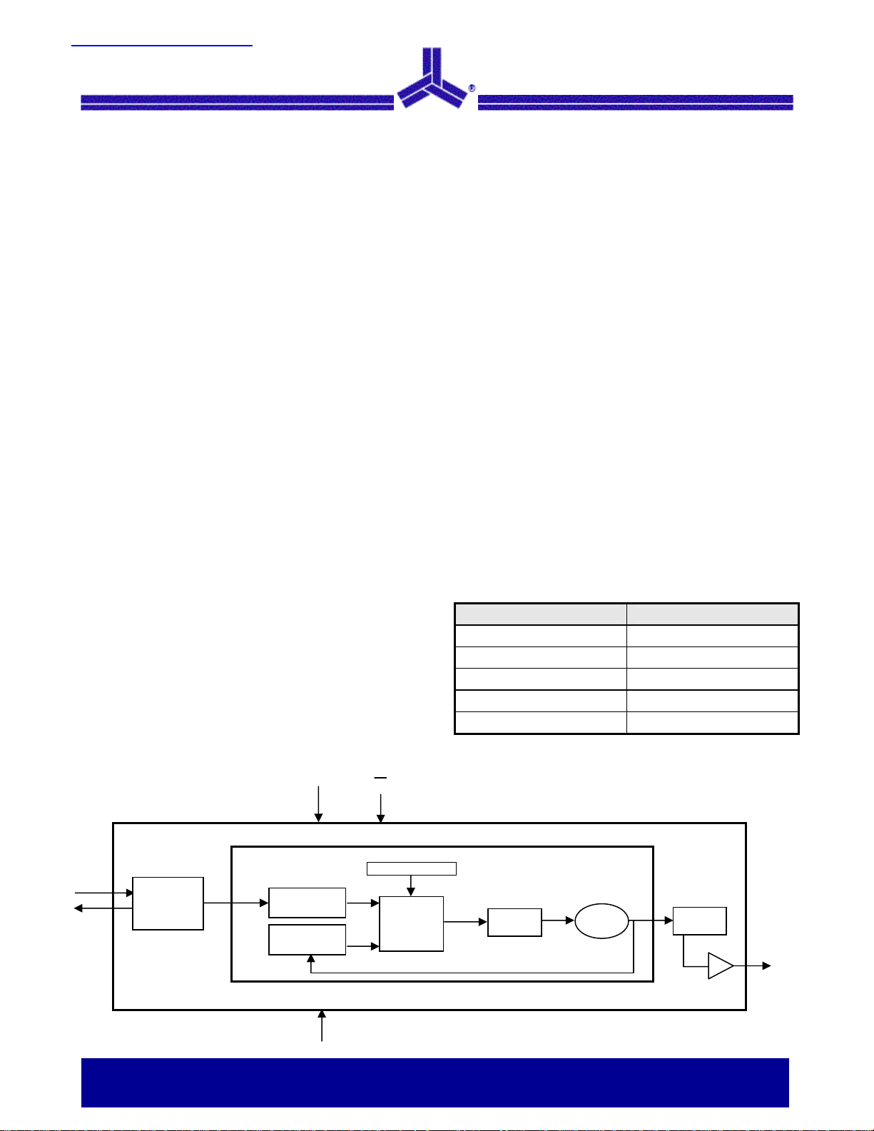
Block Diagram
VDD
PD
The ASM3P2769A uses the most efficient and optimized
modulation profile approved by the FCC and is
implemented by using a proprietary all digital method.
The ASM3P2769A modulates the output of a single PLL
in order to “spread” the bandwidth of a synthesized clock,
and more importantly, decreases the peak amplitudes of
its harmonics. This results in significantly lower system
EMI compared to the typical narrow band signal produced
by oscillators and most frequency generators. Lowering
EMI by increasing a signal’s bandwidth is called ‘spread
spectrum clock generation’.
Applications
The ASM3P2769A is targeted towards all portable
devices with very low power requirements like MP3
players and digital still cameras.
Key Specifications
Description Specification
Supply voltages VDD = 3.3V / 2.5V
Cycle-to-Cycle Jitter 200pS (Max)
Output Duty Cycle 45/55%
Modulation Rate Equation FIN/256
Frequency Deviation ±1% @ 10MHz
VCO
PLL
Output
Divide
ModOUT
XIN
XOUT
Crystal
Frequency
Divide
Feedback
Divide
VSS
Modulation
Phase
Detecto
Alliance Semiconductor
Loop
Filte
2575 Augustine Drive • Santa Clara, CA • Tel: 408.855.4900 • Fax: 408.855.4999 • www.alsc.com
Notice: The information in this document is subject to change without notice.
September 2005
ASM3P2769A
rev 1. 8
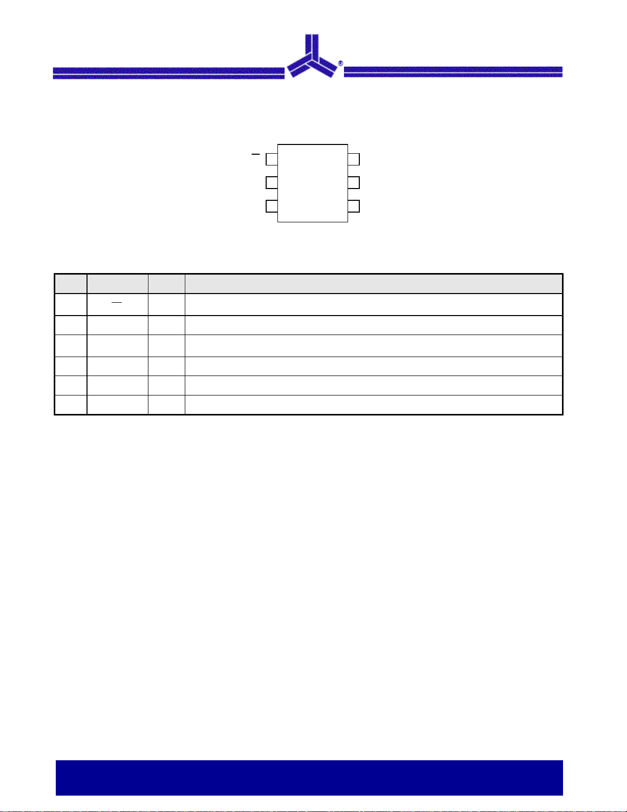
Pin Configuration (6-pin TSOT-23 Package)
XIN/CLKIN
Pin Description
Pin# Pin Name Type Description
1
2 XOUT O Crystal connection. If using an external reference, this pin must be left unconnected.
3 XIN/CLKIN I
4 VDD P Power supply for the entire chip.
PD
Power-down control pin. Pull low to enable power-down mode. Connect to VDD if not
I
used.
Crystal connection or external reference frequency input. This pin has dual functions. It
can be connected either to an external crystal or an external reference clock.
PD
XOUT
1
ASM3P2769A
2
3
6
VSS
5
ModOUT
VDD
4
5 ModOUT O Spread spectrum clock output.
6 VSS P Ground connection.
Low Power Peak EMI Reducing Solution 2 of 12
Notice: The information in this document is subject to change without notice.
September 2005
ASM3P2769A
rev 1. 8
Pin Configuration (8-pin SOIC and TSSOP Packages)
XIN/CLKIN
Pin Description
Pin# Pin Name Type Description
1 XIN/CLKIN I
2 XOUT O Crystal connection. If using an external reference, this pin must be left unconnected.
3
4 NC - No connect.
PD
Crystal connection or external reference frequency input. This pin has dual functions. It
can be connected either to an external crystal or an external reference clock.
Power-down control pin. Pull low to enable power-down mode. Connect to VDD if not
I
used.
XOUT
PD
1
2
ASM3P2769A
3
4
8
VDD
NC
7
6
ModOUT
5
VSS
5 VSS P Ground connection.
6 ModOUT O Spread spectrum clock output.
7 NC - No connect.
8 VDD P Power supply for the entire chip.
Modulation Profile
Specification
Description Specification
Frequency
Range
For 2.5V Supply 6MHz < CLKIN < 12MHz
For 3.3V Supply
Modulation Equation FIN/256
Frequency Deviation ±1% @ 10MHz
6MHz < CLKIN < 13MHz
Low Power Peak EMI Reducing Solution 3 of 12
Notice: The information in this document is subject to change without notice.
September 2005
ASM3P2769A
rev 1. 8
Absolute Maximum Ratings
Symbol Parameter Rating Unit
VDD, VIN Voltage on any pin with respect to Ground -0.5 to +7.0 V
T
Storage temperature -65 to +125 °C
STG
TA Operating temperature 0 to 70 °C
Ts Max. Soldering Temperature (10 sec) 260 °C
TJ Junction Temperature 150 °C
TDV
Note: These are stress ratings only and are not implied for functional use. Exposure to absolute maximum ratings for prolonged periods of time may affect
device reliability.
DC Electrical Characteristics for 2.5V Supply
(Test condition: All parameters are measured at room temperature (+25°C) unless otherwise stated.)
Symbol Parameter Min Typ Max Unit
VIL Input low voltage VSS-0.3 - 0.8 V
VIH Input high voltage 2.0 - VDD+0.3 V
IIL Input low current - - -35 µA
IIH Input high current - - 35 µA
I
XOUT output low current (@0.5V, VDD=2.5V) - 3 - mA
XOL
I
XOUT output high current (@1.8V, VDD=2.5V) - 3 - mA
XOH
VOL Output low voltage (VDD = 2.5 V, IOL = 8mA) - - 0.6 V
VOH Output high voltage (VDD = 2.5 V, IOH = 8mA) 1.8 - - V
IDD Static supply current * - - 10 µA
ICC Dynamic supply current (2.5V, 10MHz and with no load) - 2.5 - mA
VDD Operating Voltage 2.375 2.5 2.625 V
tON Power-up time(first locked cycle after power up)** - - 5 mS
Z
Output impedance - 50 - Ω
OUT
* XIN/CLKIN pin and PD pin are pulled low
** VDD and XIN/CLKIN input are stable; PD pin is made high from low.
AC Electrical Characteristics for 2.5V Supply
Symbol Parameter Min Typ Max Unit
CLKIN Input frequency 6 - 12 MHz
Static Discharge Voltage
(As per JEDEC STD22- A114-B)
2 KV
ModOUT Output frequency 6 - 12 MHz
Input Frequency = 6MHz - ±1.55 -
fd Frequency Deviation
%
Input Frequency = 12MHz - ±0.8 -
tLH* Output rise time (measured at 0.7V to 1.7V) 0.6 1.2 1.5 nS
tHL* Output fall time (measured at 1.7V to 0.7V) 0.4 0.9 1.1 nS
tJC Jitter (cycle to cycle) - - 200 pS
tD Output duty cycle 45 50 55 %
*tLH and tHL are measured into a capacitive load of 15pF
Low Power Peak EMI Reducing Solution 4 of 12
Notice: The information in this document is subject to change without notice.
 Loading...