

Alliance Semiconductor ASM3P18S19B Service Manual

查询ASM3P18S19B供应商查询ASM3P18S19B供应商
August 2005 ASM3P18S19B
rev 2.1
Notebook LCD Panel EMI Reduction IC
Features
FCC approved method of EMI attenuation.
Provides up to 15dB EMI reduction.
Generates a low EMI Spread Spectrum clock and a
non-spread reference clock of the input frequency.
Optimized for Frequency range from 20 to 40MHz.
Internal loop filter minimizes external components and
board space.
Low Inherent Cycle-to-Cycle jitter.
Two spread % selections: -1.25% to -1.75%.
3.3V Operating Voltage.
Low power CMOS design.
Supports notebook VGA and other LCD timing
controller applications.
Power Down function for mobile application.
Available in Commercial temperature range.
Available in 8-pin SOIC and TSSOP Packages.
RoHS Compliant
Product Description
The ASM3P18S19B is a Versatile Spread Spectrum
Frequency Modulator designed specifically for input clock
frequencies from 20 to 40MHz. (Refer Input Frequency and
Modulation Rate Table). The ASM3P18S19B reduces
electromagnetic interference (EMI) at the clock source,
allowing system wide reduction of EMI of down stream
clock and data dependent signals. The ASM3P18S19B
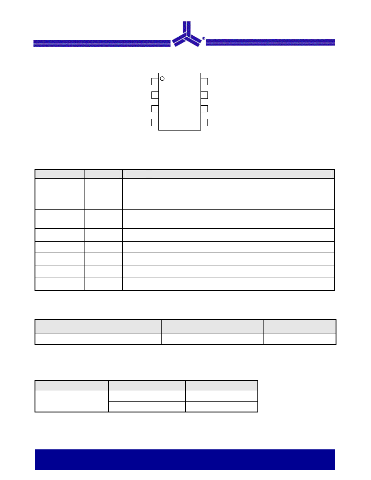
Block Diagram
PD#
allows significant system cost savings by reducing the
number of circuit board layers, ferrite beads, shielding, and
other passive components that are traditionally required to
pass EMI regulations.
The ASM3P18S19B modulates the output of a single PLL
in order to “spread” the bandwidth of a synthesized clock,
and more importantly, decreases the peak amplitudes of its
harmonics. This results in significantly lower system EMI
compared to the typical narrow band signal produced by
oscillators and most frequency generators. Lowering EMI
by increasing a signal’s bandwidth is called ‘Spread
Spectrum Clock Generation’.
The ASM3P18S19B uses the most efficient and optimized
modulation profile approved by the FCC and is
implemented in a proprietary all digital method.
Applications
The ASM3P18S19B is targeted towards EMI management
for memory and LVDS interfaces in mobile graphic chipsets
and high-speed digital applications such as PC peripheral
devices, consumer electronics, and embedded controller
systems.
SRS
VDD
PLL
VCO
XIN/CLKIN
XOUT
REF
Crystal
Oscillator
Frequency
Divider
Feedback
Divider
Modulation
Phase
Detector
Alliance Semiconductor
Loop
Filter
VSS
2575 Augustine Drive • Santa Clara, CA • Tel: 408.855.4900 • Fax: 408.855.4999 • www.alsc.com
Notice: The information in this document is subject to change without notice.
Output
Divider
ModOUT
August 2005
ASM3P18S19B
rev 2.1
Pin Configuration
Pin Description
Pin# Pin Name Type Description
1 XIN / CLKIN I
2 VSS P Ground Connection. Connect to system ground.
3 SRS I
4 ModOUT O
5 REF O Non-modulated Reference clock output of the input frequency.
6 PD# I
7 VDD P Power Supply for the entire chip.
8 XOUT O
Input Frequency and Modulation Rate
XIN/ CLKIN
VSS
SRS
ModOUT
1
2
ASM3P18S19B
3
4
Crystal Connection or external frequency input.This pin has dual
functions. It can be connected to either an external crystal or an external
reference clock
Spread range select. Digital logic input used to select frequency deviation
(Refer Spread Deviation Selection Table). This pin has an internal pull-up
resistor.
Spread spectrum clock output. (Refer Input Frequency and Modulation
Rate Table and Spread Deviation Selection Table)
Power down control pin. Pull LOW to enable Power-Down mode. This pin
has an internal pull-up resistor.
Crystal Connection. Input connection for an external crystal. If using an
external reference, this pin must be left unconnected.
XOUT
8
7
VDD
6
PD#
REF
5
Part Number Input Frequency Range Output Frequency range Modulation rate
ASM3P18S19B 20MHz to 40MHz 20MHz to 40MHz Input Frequency / 512
Spread Deviation Selection
Part Number SRS Spread Deviation
ASM3P18S19B
0 -1.25% (DOWN)
1 -1.75% (DOWN)
Notebook LCD Panel EMI Reduction IC 2 of 7
Notice: The information in this document is subject to change without notice.
August 2005
ASM3P18S19B
rev 2.1
Absolute Maximum Ratings
Symbol Parameter Rating Unit
VDD, VIN Voltage on any pin with respect to Ground -0.5 to +7.0 V
T
Storage temperature -65 to +125 °C
STG
TA Operating temperature 0 to 70 °C
Ts Max. Soldering Temperature (10 sec) 260 °C
TJ Junction Temperature 150 °C
TDV
Note: These are stress ratings only and are not implied for functional use. Exposure to absolute maximum ratings for prolonged periods of time may affect
device reliability.
DC Electrical Characteristics
(Test condition: All parameters are measured at room temperature (+25°C) unless otherwise stated)
Symbol Parameter Min Typ Max Unit
VIL Input Low voltage VSS - 0.3 - 0.8 V
VIH Input High voltage 2.0 - VDD + 0.3 V
IIL Input Low current (inputs PD#, SRS) -60.0 - -20.0 µA
Static Discharge Voltage
(As per JEDEC STD22- A114-B)
2 KV
IIH Input High current - - 1.0 µA
I
X
XOL
I
X
XOH
Output low current @ 0.4V, VDD = 3.3V - 3 - mA
OUT
Output high current @ 2.5V, VDD = 3.3V - 3 - mA
OUT
VOL Output Low voltage VDD = 3.3V, IOL = 20mA - - 0.4 V
VOH Output High voltage VDD = 3.3V, IOH = 20mA 2.5 - - V
ICC
Dynamic supply current normal mode
3.3V and 25pF probe loading
fIN
7.1
- min
-
26.9
f
IN - max
mA
IDD Static supply current standby mode - 4.5 - mA
VDD Operating Voltage - 3.3 - V
tON Power up time (first locked clock cycle after power up) - 0.18 - mS
Z
Clock Output impedance - 50 - Ω
OUT
AC Electrical Characteristics
Symbol Parameter Min Typ Max Unit
fIN Input Frequency 20 - 40 MHz
f
Output Frequency 20 - 40 MHz
OUT
tLH*
tHL*
tJC Jitter (Cycle to Cycle) -200 - 200 pS
tD Output Duty cycle 45 50 55 %
Output Rise time
Measured from 0.8V to 2.0V
Output Fall time
Measured from 0.8V to 2.0V
- 0.66 - nS
- 0.65 - nS
*tLH and tHL are measured into a capacitive load of 15pF
Notebook LCD Panel EMI Reduction IC 3 of 7
Notice: The information in this document is subject to change without notice.
 Loading...