

Alliance Semiconductor AS7C513, AS7C3513 Service Manual
查询AS7C3513-12供应商
March 2001
Features
• AS7C513 (5V version)
• AS7C3513 (3.3V version)
• Industrial and commercial temperature
• Organization: 32,768 words × 16 bits
• Center power and ground pins
•High speed
- 12/15/20 ns address access time
- 6,7,8 ns output enable access time
• Low power consumption: ACTIVE
- 800 mW (AS7C513) / max @ 12 ns
- 432 mW (AS7C3513) / max @ 12 ns
®
5V/3.3V 32K×16 CMOS SRAM
• Low power consumption: STANDBY
- 28 mW (AS7C513) / max CMOS
- 18 mW (AS7C3513) / max CMOS
• 2.0V data retention
• Easy memory expansion with CE
• TTL-compatible, three-state I/O
• 44-pin JEDEC standard package
-400 mil SOJ
-400 mil TSOP II
• ESD protection ≥ 2000 volts
• Latch-up current ≥ 200 mA
AS7C513
AS7C3513
, OE inputs
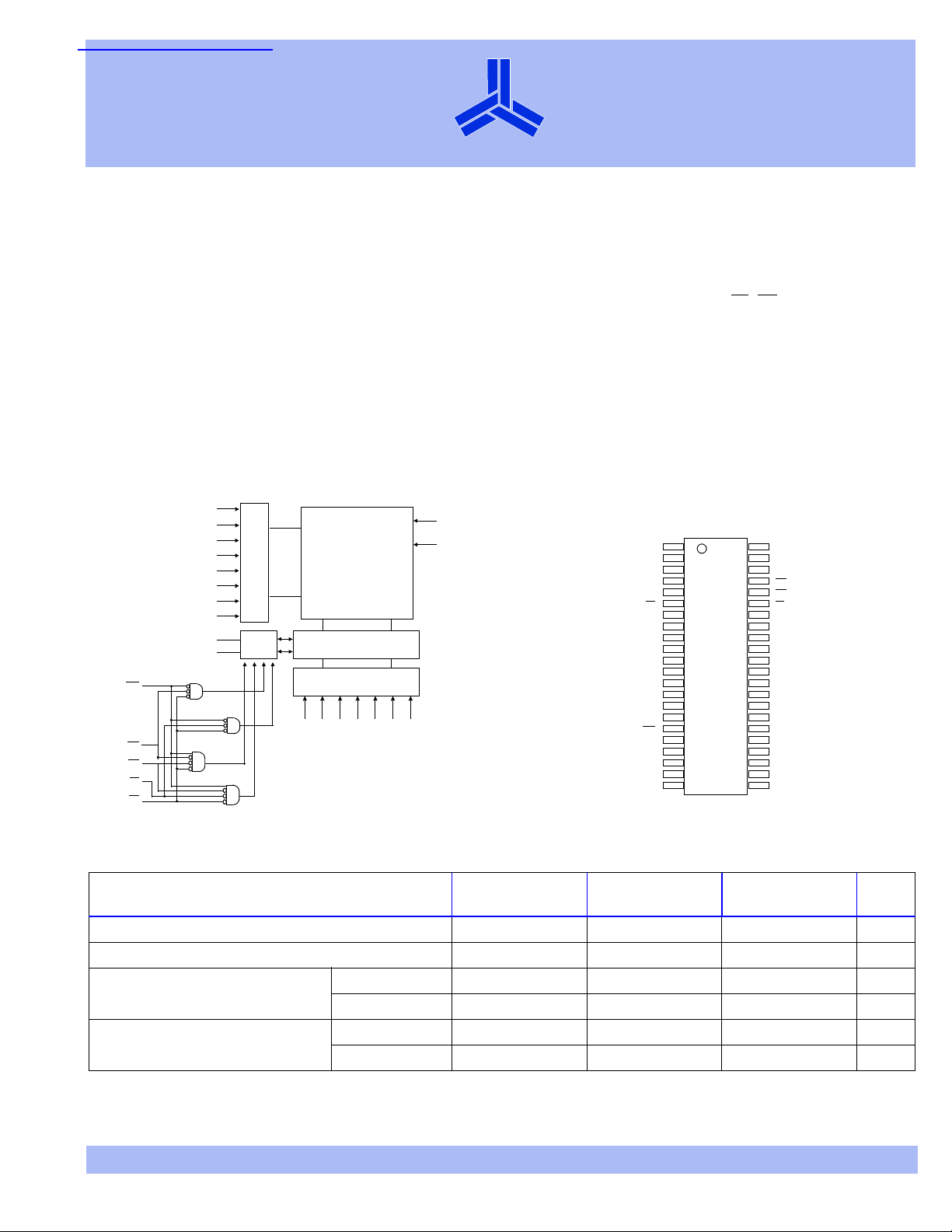
Logic block diagram
A0
A1
A2
A3
A4
A5
A6
A7
I/O0–I/O7
I/O8–I/O15
WE
UB
OE
LB
CE
Row decoder
I/O
buffer
32K × 16
Array
Control circuit
Column decoder
A8
A9
A10
A11
A12
A13
A14
V
CC
GND
Pin arrangement
44-Pin SOJ, TSOP II (400 mil)
1NC
44
A4
43
A5
42
A6
41
OE
UB
40
LB
39
I/O15
38
I/O14
37
I/O13
36
I/O12
35
GND
34
V
33
CC
I/O11
32
I/O10
31
I/O9
30
I/O8
29
NC
28
A7
27
A8
26
A9
25
A10
24
NC
23
I/O0
I/O1
I/O2
I/O3
V
GND
I/O4
I/O5
I/O6
I/O7
WE
A14
A13
A12
A11
2A3
3A2
4A1
5
A0
6
CE
7
8
9
10
11
CC
12
13
AS7C513
AS7C3513
14
15
16
17
18
19
20
21
22
NC
Selection guide
AS7C513-12
AS7C3513-12
Maximum address access time 12 15 20 ns
Maximum output enable access time 5 7 9 ns
AS7C513 160 150 140 mA
Maximum operating current
AS7C3513 120 110 100 mA
AS7C513 5 5 5 mA
Maximum CMOS standby current
AS7C3513 5 5 5 mA
Shaded areas indicate advance information.
AS7C513-15
AS7C3513-15
AS7C513-20
AS7C3513-20 Unit
3/23/01; v.1.0
Alliance Semiconductor
P. 1 of 10
Copyright © Alliance Semiconductor. All rights reserved.

AS7C513
AS7C3513
®
Functional description
The AS7C513 and the AS7C3513 are high performance CMOS 524,288-bit Static Random Access Memory (SRAM) devices organized as
32,768 words × 16 bits. They are designed for memory applications where fast data access, low power, and simple interfacing are desired.
Equal address access and cycle times (tAA, tRC, tWC) of 12/15/20 ns with output enable access times (tOE) of 6,7,8 ns are ideal for high
performance applications. The chip enable input CE
When CE
consumption in CMOS standby mode. The devices also offer 2.0V data retention.
A write cycle is accomplished by asserting write enable (WE), (UB) and/or (LB), and chip enable (CE). Data on the input pins I/O0-I/O7,
and/or I/O8–I/O15, is written on the rising edge of WE
should drive I/O pins only after outputs have been disabled with output enable (OE
A read cycle is accomplished by asserting output enable (OE
drive I/O pins with the data word referenced by the input address. When either chip enable or output enable is inactive, or write enable is
active, or (UB) and (LB), output drivers stay in high-impedance mode.
The devices provide multiple center power and ground pins, and separate byte enable controls, allowing individual bytes to be written and
read. LB controls the lower bits, I/O0–I/O7, and UB controls the higher bits, I/O8–I/O15.
All chip inputs and outputs are TTL-compatible. The AS7C513 and AS7C3513 are packaged in common industry standard packages.
is high, the devices enter standby mode. The AS7C513 and AS7C3513 are guaranteed not to exceed 28/18 mW power
permits easy memory expansion with multiple-bank memory systems.
(write cycle 1) or CE (write cycle 2). To avoid bus contention, external devices
) or write enable (WE).
), (UB) and (LB), and chip enable (CE), with write enable (WE) high. The chips
Absolute maximum ratings
Parameter Device Symbol Min Max Unit
Vo l t ag e o n V
relative to GND
CC
AS7C3513 V
Voltage on any pin relative to GND V
Power dissipation P
Storage temperature (plastic) T
AS7C513 V
Ambient temperature with V
applied T
CC
DC current into outputs (low) I
NOTE: Stresses greater than those listed under Absolute Maximum Ratings may cause permanent damage to the device. This is a stress rating only and functional
operation of the device at these or any other conditions outside those indicated in the operational sections of this specification is not implied. Exposure to
absolute maximum rating conditions for extended periods may affect reliability.
t1
t1
t2
D
stg
bias
OUT
–0.50 +7.0 V
–0.50 +5.0 V
–0.50 VCC +0.50 V
–1.0W
–65 +150
–55 +125
o
C
o
C
–50mA
Truth table
CE
H X X X X High Z High Z Standby (I
LHLLHD
LHLHLHigh ZD
LHLLLD
LLXLLD
LLXLHD
LLXHLHigh ZD
L
L
Key: X = Don’t care; L = Low; H = High
3/23/01; v. 1.0
WE OE LB UB I/O0–I/O7 I/O8–I/O15 Mode
OUT
OUT
IN
IN
H
X
H
X
X
H
X
H
High Z High Z Output disable (I
High Z Read I/O0–I/O7 (ICC)
Read I/O8–I/O15 (ICC)
Read I/O0–I/O15 (ICC)
Write I/O0–I/O15 (ICC)
D
D
OUT
OUT
IN
High Z Write I/O0–I/O7 (ICC)
IN
Write I/O8–I/O15 (ICC)
Alliance Semiconductor
, I
)
SB
SBI
)
CC
P. 2 of 10
AS7C513
AS7C3513
®
Recommended operating conditions
Parameter Device Symbol Min Typical Max Unit
Supply voltage
Input voltage
commercial T
Ambient operating temperature
industrial T
†
VIL min = –3.0V for pulse width less than tRC/2.
AS7C513 V
AS7C3513 V
AS7C513 V
AS7C3513 V
CC
CC
IH
IH
V
IL
A
A
4.5 5.0 5.5 V
3.0 3.3 3.6 V
2.2 – VCC + 0.5 V
2.0 – VCC + 0.5
–0.5†–0.8V
0– 70 ° C
–40 – 05 ° C
DC operating characteristics (over the operating range)1
-12 -15 -20
Parameter Symbol Test conditions Device
Input leakage current | I
Output leakage current | I
Operating power supply
current
|
LI
|
LO
I
CC
I
SB
Standby power supply
current
I
SB1
V
Output voltage
Shaded areas indicate advance information.
OL
V
OH
V
= Max
CC
V
= GND to V
IN
V
= Max
CC
V
= GND to V
OUT
V
= Max, CE ≤ V
CC
f = f
V
f = f
V
V
V
, I
Max
OUT
= Max, CE ≤ V
CC
, I
Max
OUT
= Max, CE ≥ V
CC
≤ GND + 0.2V or
IN
≥ V
IN
–0.2V, f = 0
CC
CC
CC
IL
= 0mA
IL
= 0mA
CC
–0.2V
AS7C513 – 160 – 150 – 140
AS7C3513 – 120 – 110 – 100
AS7C513 – 40 – 40 – 40
AS7C3513 – 40 – 40 – 40
AS7C513 – 3 – 3 – 3
AS7C3513–3–3–3
–1–1–1µA
–1–1–1µA
IOL = 8 mA, VCC = Min – 0.4 – 0.4 – 0.4 V
IOH = –4 mA, VCC = Min 2.4–2.4–2.4– V
UnitMin Max Min Max Min Max
mA
mA
mA
Capacitance (f = 1MHz, Ta = 25o C, VCC = NOMINAL)
2
Parameter Symbol Signals Test conditions Max Unit
Input capacitance C
I/O capacitance C
3/23/01; v. 1.0
IN
I/O
A, CE, WE, OE, LB, UB
I/O Vin = V
Alliance Semiconductor
Vin = 0V 5 pF
= 0V 7 pF
out
P. 3 of 10
 Loading...