

Alliance Semiconductor AS7C33128FT18B Service Manual
December 2004
3.3V 128K × 18 Flow Through Synchronous SRAM
Features
• Organization: 131,072 words × 18 bits
• Fast clock to data access: 6.5/7.5/8.0/10.0 ns
•Fast OE
• Fully synchronous flow through operation
• Asynchronous output enable control
• Economical 100-pin TQFP package
• Individual byte write and Global write
• Multiple chip enables for easy expansion
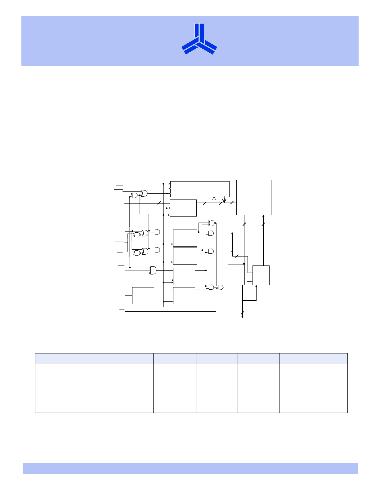
Logic block diagram
access time: 3.5/4.0 ns
CLK
ADV
ADSC
ADSP
A[16:0]
17
D
CS
CLK
CLK
CS
CLR
Burst logic
Address
register
AS7C33128FT18B
®
• 3.3V core power supply
• 2.5V or 3.3V I/O operation with separate V
• Linear or interleaved burst control
• Snooze mode for reduced power standby
• Common data inputs and data outputs
LBO
128K × 18
Memory
2
2
Q
17
15
17
array
DDQ
GWE
BW
BWE
BW
CE0
CE1
CE2
DQ
18
b
a
Power
ZZ
down
OE
DQb
Byte Write
registers
CLK
DQ
DQa
Byte Write
registers
CLK
DQ
Enable
register
CE
CLK
DQ
Enable
delay
register
CLK
OE
Output
Buffers
2
18
Input
registers
CLK
18
DQ [a,b]
Selection guide
–65 -75 -80 -10 Units
Minimum cycle time 7.5 8.5 10 12 ns
Maximum clock access time 6.5 7.5 8.0 10.0 ns
Maximum operating current 250 225 200 175 mA
Maximum standby current 120 100 90 90 mA
Maximum CMOS standby current (DC) 30 30 30 30 mA
12/10/04; v.1.3 Alliance Semiconductor P. 1 of 19
Copyright © Alliance Semiconductor. All rights reserved.
AS7C33128FT18B
®
2 Mb Synchronous SRAM products list
Org Part Number Mode Speed
128KX18 AS7C33128PFS18B PL-SCD 200/166/133 MHz
64KX32
64KX36 AS7C3364PFS36B PL-SCD 200/166/133 MHz
128KX18 AS7C33128PFD18B PL-DCD 200/166/133 MHz
64KX32
64KX36 AS7C3364PFD36B PL-DCD 200/166/133 MHz
128KX18 AS7C33128FT18B FT 6.5/7.5/8.0/10 ns
64KX32
64KX36 AS7C3364FT36B FT 6.5/7.5/8.0/10 ns
AS7C3364PFS32B PL-SCD 200/166/133 MHz
AS7C3364PFD32B PL-DCD 200/166/133 MHz
AS7C3364FT32B FT 6.5/7.5/8.0/10 ns
1,2
1 Core Power Supply: VDD = 3.3V + 0.165V
2 I/O Supply Voltage: VDDQ = 3.3V +
VDDQ = 2.5V +
0.165V for 3.3V I/O
0.125V for 2.5V I/O
PL-SCD : Pipelined Burst Synchronous SRAM - Single Cycle Deselect
PL-DCD : Pipelined Burst Synchronous SRAM - Double Cycle Deselect
FT : Flow-through Burst Synchronous SRAM
12/10/04; v.1.3 Alliance Semiconductor P. 2 of 19
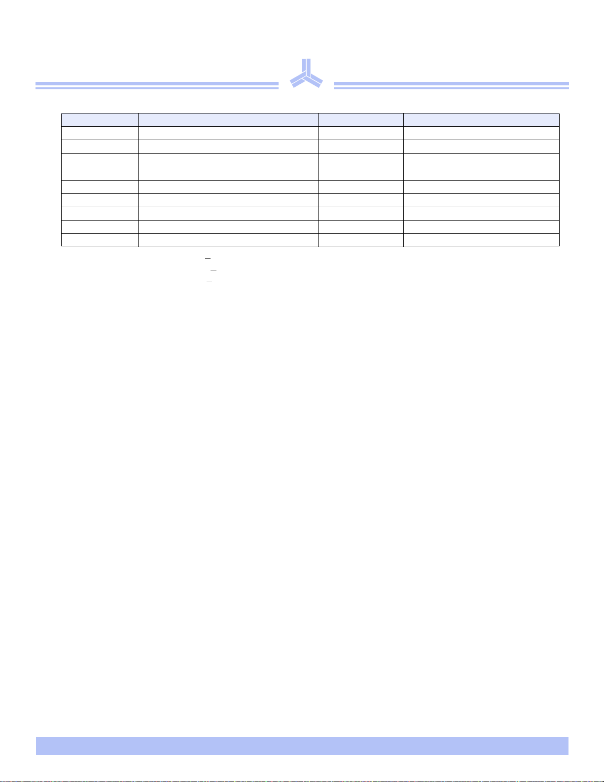
Pin arrangement
V
DDQ
V
DQb0
DQb1
V
V
DDQ
DQb2
DQb3
V
DQb4
DQb5
V
DDQ
V
DQb6
DQb7
DQpb
V
V
DDQ
NC
NC
NC
SSQ
NC
NC
SSQ
NC
DD
NC
V
SSQ
NC
SSQ
NC
NC
NC
SS
®
DD
SS
AACE0
100
CE1NCNC
BWb
99989796959493929190898887868584838281
V
BWa
CE2
V
CLK
GWE
BWEOEADSC
1
2
3
4
5
6
7
8
9
10
11
12
13
14
15
TQFP 14 × 20mm
16
17
18
19
20
21
22
23
24
25
26
27
28
29
30
31323334353637383940414243444546474849
ADSP
ADVAA
AS7C33128FT18B
80
79
78
77
76
75
74
73
72
71
70
69
68
67
66
65
64
63
62
61
60
59
58
57
56
55
54
53
52
51
50
A
NC
NC
V
DDQ
V
SSQ
NC
DQpa
DQa7
DQa6
V
SSQ
V
DDQ
DQa5
DQa4
VSS
NC
V
DD
ZZ
DQa3
DQa2
V
DDQ
V
SSQ
DQa1
DQa0
NC
NC
V
SSQ
V
DDQ
NC
NC
NC
AAA
LBO
12/10/04; v.1.3 Alliance Semiconductor P. 3 of 19
A
A1
A0
NC
NC
V
SS
V
DD
AAAAA
NC
NC
A
NC
AS7C33128FT18B
®
Functional description
The AS7C33128FT18B is a high-performance CMOS 2-Mbit synchronous Static Random Access Memory (SRAM) device organized as
131,072 words × 18 bits.
Fast cycle times of 7.5/8.5/10/12 ns with clock access times (tCD) of 6.5/7.5/8.0/10 ns. Three chip enable (CE) inputs permit easy memory
expansion. Burst operation is initiated in one of two ways: the controller address strobe (ADSC
The burst advance pin (ADV) allows subsequent internally generated burst addresses.
Read cycles are initiated with ADSP (regardless of WE and ADSC) using the new external address clocked into the on-chip address
register when ADSP is sampled low , the chip enables are sa mpled active, and the ou tput buffe r is enabled with OE. In a read operation, the
data accessed by the current address registered in the address registers by the positive edge of CLK are carried to the data-out buffer. ADV
is ignored on the clock edge that samples ADSP asserted, but is sampled on all subsequent clock edges. Address is incremented internally
for the next access of the burst when ADV is sampled low and both address strobes are high. Burst mode is selectable with the
LBO
With
unconnected or driven high, burst operations use an interleaved count sequence. With
count sequence.
Write cycles ar e perform ed by d isabling the output buffers with OE and asserting a write command. A global write enable GWE writes all
18 bits regardless of the state of individual BW[a,b] inputs. Alternately, when GWE is high, one or more bytes may be written by asserting
BWE and the appropriate individual byte BWn signals.
BWn is ignored on the clock edge that samples ADSP low, but it is sampled on all subsequent clock edges. Output buffers are disabled
when BWn is sampled LOW regardless of OE. Data is clocked into the data input register when BWn is sampled low. Address is
incremented internally to the next burst address if BWn
Read or write cycles may also be initiated with ADSC
and ADV are sampled low.
instead of ADSP. The differences between cycles initiated with ADSC and ADSP
are as follows:
• ADSP
must be sampled high when ADSC is sampled low to initiate a cycle with ADSC.
), or the processor address strobe (ADSP).
LBO
input.
LBO
driven low, the device uses a linear
•WE signals are sampled on the clock edge that samples ADSC low (and ADSP high).
• Master chip enable CE0 blocks ADSP, but not ADSC.
The AS7C33128FT18B family operates from a core 3.3V power supply. I/Os use a separate power supply that can operate at 2.5V or 3.3V.
These devices are available in a 100-pin TQFP package.
TQFP capacitance
Parameter Symbol Test conditions Min Max Unit
Input capacitance C
I/O capacitance C
*Guaranteed not tested
IN
I/O
*
*
VIN = 0V - 5 pF
V
= 0V - 7 pF
OUT
TQFP thermal resistance
Description Conditions Symbol Typical Units
Thermal resistance
(junction to ambient)
Thermal resistance
(junction to top of case)
1 This parameter is sampled
1–layer θ
1
1
Test conditio ns follow standard test methods and
procedures for measuring thermal impedance,
per EIA/JESD51
4–layer θ
JA
JA
θ
JC
40 °C/W
22 °C/W
8 °C/W
12/10/04; v.1.3 Alliance Semiconductor P. 4 of 19

Signal descriptions
AS7C33128FT18B
®
Pin I/O Properties
Description
CLK I CLOCK Clock. All inputs except OE, ZZ, and LBO are synchronous to this clock.
A,A0,A1 I SYNC Address. Sampled when all chip enables are active and when ADSC or ADSP are asserted.
DQ[a,b] I/O SYNC Data. Driven as output when the chi p is enabled and when OE
CE0 I SYNC
CE1, CE2
ADSP
ADSC
ADV
GWE
I SYNC
I SYNC Address strobe processor. Asserted low to load a new address or to enter standby mode.
I SYNC Address strobe controller. Asserted low to load a new address or to enter standby mode.
I SYNC Advance. Asserted low to continue burst read/write.
I SYNC
Master chip enable. Sampled on clock edges when ADSP
ADSP is blocked. Refer to the “Synchronous truth table” for more information.
Synchronous chip enables, active high, and active low, respectively . Sampled on clock edges when
is active or when CE0 and ADSP are active.
ADSC
Global write enable. Asserted low to write all 18 bits. When high, BWE
enable.
is active.
or ADSC is active. When CE0 is inactive,
and BW[a,b] control write
BWE I SYNC Byte write enable. Asserted low with GWE high to enable effect of BW[a,b] inputs.
Write enables. Used to control write of individual bytes when GWE is high and BWE is low. If any of
BW[a,b]
I SYNC
BW[a,b] is active with GWE high and BWE low , the cy cle is a write cyc le. If all BW[a ,b] are in active ,
the cycle is a read cycle.
OE
LBO ISTATIC
I ASYNC Asynchronous output enable. I/O pins are driven when OE is active and chip is in read mode.
Selects Burst mode. When tied to V
or left floating, device follows interleaved Burst order. When
DD
driven Low, device follows linear Burst order. This signal is internally pulled High.
ZZ I ASYNC Snooze. Places device in low power mode; data is retained. Connect to GND if unused.
NC - - No connect
Snooze Mode
SNOOZE MODE is a low current, power-down mode in which the device is deselected and current is reduced to I
SNOOZE MODE is dictated by the length of time the ZZ is in a High state.
The ZZ pin is an asynchronous, active high input that causes the device to enter SNOOZE MODE.
When the ZZ pin becomes a logic High, I
is guaranteed after the time t
SB2
is met. After entering SNOOZE MODE, all inputs except ZZ
ZZI
is disabled and all outputs go to High-Z. Any operation pending when entering SNOOZE MODE is not guaranteed to successfully complete. Therefore, SNOOZE MODE (READ or WRITE) must not be initiated until valid pending operations are completed. Similarly, when
exiting SNOOZE MODE during t
, only a DESELECT or READ cycle should be given while the SRAM is transitioning out of SNOOZE
PUS
MODE.
12/10/04; v.1.3 Alliance Semiconductor P. 5 of 19
. The duration of
SB2
®
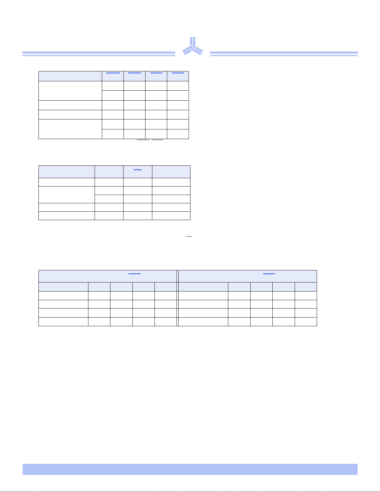
Write enable truth table (per byte)
Function GWE BWE BWa BWb
Write All Bytes
Write Byte a
Write Byte b
Read
Key: X = don’t care, L = low, H = high, n = a, b;
LXXX
HLLL
HLLH
HLHL
HHXX
HLHH
BWE, BWn
= internal write signal.
Asynchronous Truth Table
Operation ZZ OE I/O Status
Snooze mode H X High-Z
Read
Write L X Din, High-Z
Deselected L X High-Z
Notes:
1. X means “Don’t Care”
2. ZZ pin is pulled down internally
3. For write cycles that follows read cycles, the output buffers must be disabled with OE
4. Snooze mode means power down state of which stand-by current does not depend on cycle times
5. Deselected means power down state of which stand-by current depends on cycle times
LLDout
L H High-Z
, otherwise data bus contention will occur.
AS7C33128FT18B
Burst sequence table
Interleaved burst address (LBO = 1) Linear burst address (LBO = 0)
A1 A0 A1 A0 A1 A0 A1 A0 A1 A0 A1 A0 A1 A0 A1 A0
1st Address
nd
2
Address
rd
3
Address
th
4
Address
0 00 11 01 1
0 10 01 11 0
1 01 10 00 1
1 11 00 10 0
1st Address
nd
2
Address
rd
3
Address
th
4
Address
0 00 11 01 1
0 11 01 10 0
1 01 10 00 1
1 11 00 11 0
12/10/04; v.1.3 Alliance Semiconductor P. 6 of 19
 Loading...