

Alliance Semiconductor AS7C256, AS7C256L Service Manual
查询7C256供应商
High Performance
32K×8
CMOS SRAM
FEATURES
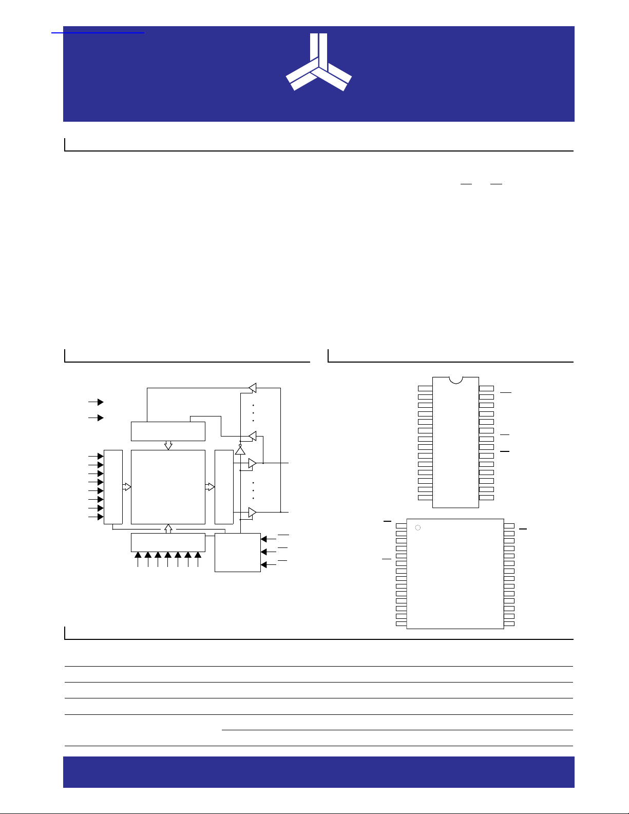
• Organization: 32,768 words × 8 bits
• High speed
– 10/12/15/20/25/35 ns address access time
– 3/3/4/5/6/8 ns output enable access time
• Low power consumption
– Active: 660 mW max (10 ns cycle)
– Standby: 11 mW max, CMOS I/O
2.75 mW max, CMOS I/O, L version
– Very low DC component in active power
• 2.0V data retention (L version)
32K×8 CMOS SRAM (Common I/O)
• Equal access and cycle times
• Easy memory expansion with CE
• TTL-compatible, thre e-sta te I/O
• 28-pin JEDEC standard packages
– 300 mil PDIP and SOJ
Socket compatible with 7C512 and 7C1024
– 330 mil SOIC
–8×13.4 TSOP
• ESD protection > 2000 volts
• Latch-up current > 200 mA
AS7C256
AS7C256L
and OE inputs
LOGIC BLOCK DIAGRAM
Vcc
GND
INPUT BUFFER
A0
A1
A2
A3
A4
A5
A6
A14
ROW DECODER
256×128×8
ARRAY
(262,144)
COLUMN DECODER
A8A
A9A10A11A12A
7
SELECTION GUIDE
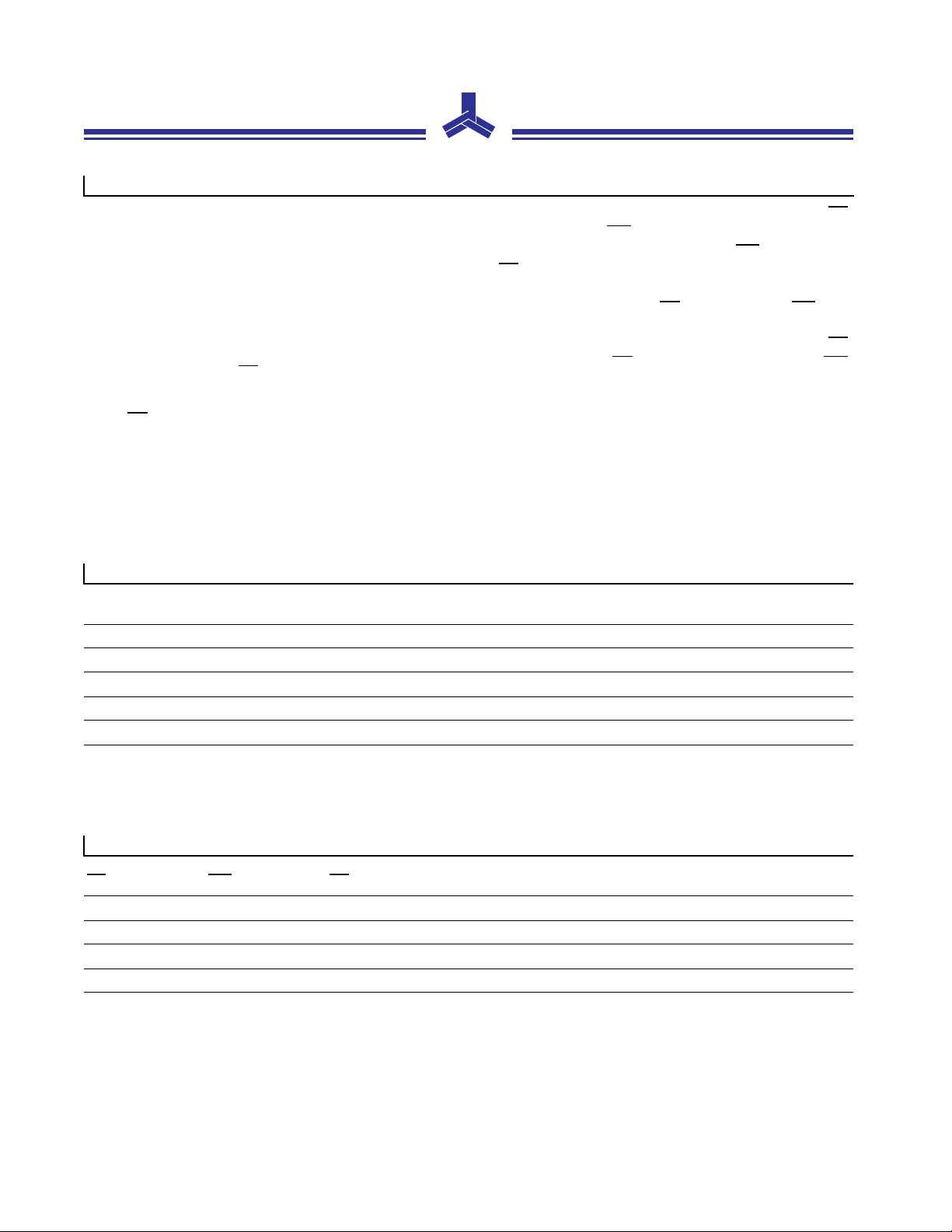
PIN ARRANGEME NT
DIP, SOJ, SOIC
I/O7
SENSE AMP
CONTROL
CIRCUIT
13
WE
OE
CE
I/O0
TSOP 8×13.4
A14
A12
A7
A6
A5
A4
A3
A2
A1
A0
I/O0
I/O1
I/O2
GND
OE A10
A11
A9
A8
A13
WE
Vcc
A14
A12
A7
A6
A5
A4
A3 A2
1
2
3
4
5
6
7
8
9
AS7C256
10
11
12
13
14
22
23
24
25
26
27
28
AS7C256
1
2
3
4
5
6
7
Vcc
28
WE
27
26
A13
25
A8
24
A9
23
A11
OE
22
A10
21
20
CE
19
I/O7
18
I/O6
17
I/O5
16
I/O4
15
I/O3
21
CE
20
I/O7
19
I/O6
18
I/O5
17
I/O4
16
I/O3
15
14
GND
13
I/O2
12
I/O1
11
I/O0
10
A0
9
8
AS7C256-02AS7C256-01
A1
7C256-10 7C256-12 7C256-15 7C256-20 7C256-25 7C256-35 Unit
Maximum Address Access Time 10 12 15 20 25 35 ns
Maximum Output Enable Access Time 334568ns
Maximum Operating Current 120 115 110 100 90 80 mA
Maximum CMOS Standby Current
2.0 2.0 2.0 2.0 2.0 2.0 mA
L 0.5 0.5 0.5 0.5 0.5 0.5 mA
ALLIANCE SEMICONDUCTOR
AS7C256
AS7C256L
FUNCTIONAL DESCRIPTION
The AS7C256 is a high performance CMOS 262,144-bit
Static Random Access Memory (SRAM) organized as
32,768 words × 8 bits. It is designed for memory applications where fast data access, low power, and simple interfacing are desired.
Equal address access and cycle times (t
, tRC, tWC) of
AA
10/12/15/20/25/35 ns with output enable access times (t
of 3/3/4/5/6/8 ns are ideal for high performance applications. A chip enable (CE
) input permits easy memory
expansion with mult iple-bank memory organizations.
When CE
is HIGH the device enters standby mode. The
standard AS7C256 is guaranteed not to exceed 11 mW
A write cycle is accomplishe d by asserti n g chip enable (CE
and write enable (WE
) LOW. Data on the input pins
I/O0-I/O7 is writt en on the r ising edge of WE
(write cycle 2). To avoid bus contention, external
or CE
devices should drive I/O pins only after outputs have been
disabled with output enable (OE
)
OE
A read cycle is accompl ished by assert ing chip enable (CE
and output enable (OE
) LOW, with write enable (WE)
) or write enable (WE).
HIGH. The chip drives I/O pins with the data word referenced by the input address. When chip enable or output
enable is HIGH, or wri te enable is LOW, output drivers stay
in high-impedance mode.
(write cycle 1)
power consumption in standby mode; the L version is guaranteed not to exceed 2.75 mW, and typically requires only
500 µW. The L version also offers 2.0V data retention, with
maximum power consumption in this mode of 300 µW.
All chip inputs and outputs are TTL-compa tible, and operation is from a single 5V supply. The AS7C256 is packaged
in all high volume industry standard packages.
ABSOLUTE MAXIMUM RATINGS
Parameter Symbol Min Max Unit
Voltage on Any Pin Relative to G N D V
Power Dissipation P
Storage Temperature (Plastic) T
Temperatur e Under Bias T
DC Output Current I
NOTE: Stresses greater than those listed under Absolute Maximum Ratings may cause permanent damage to the device. This is a stress
rating only and functional operatio n of the device at these or any other conditions outside those indicated in the operationa l sections of
this specification is not implied. Exposure to absolute maximum rating conditions for extended periods may affect reliability.
.
t
D
stg
bias
out
–0.5 +7.0 V
– 1.0 W
–55 +150
–10 +85
–20mA
o
C
o
C
)
)
TRUT H TABLE
CE
HXXHigh Z Standby (I
L H H High Z Output Disable
LHLD
LLXD
Key: X = Don’t Care, L = LOW, H = HIGH
WE OE Data Mode
out
in
Read
Write
SB
, I
)
SB1
2
AS7C256
AS7C256L
RECOMMEND ED OPER ATING C ONDITI ONS (Ta = 0°C to +70°C)
Parameter Symbol Min Typ Max Unit
Supply Voltage
Input Voltage
min = –3.0V for pulse width less than tRC/2.
*V
IL
DC OPERATING CHARACTERISTICS
Parameter Symbol Test Conditions
Input Leakage
Current
Output Leakage
Current
Operating Power
Supply Current
Standby
Power Supply
Current
Output Voltage
|ILI|
|ILO|
I
CC
I
SB
I
SB1
V
V
VCC = Max,
V
= GND to V
in
CE = VIH, VCC = Max,
V
= GND to V
out
CE = VIL, f = f
I
= 0 mA
out
CE = VIH, f = f
CE > VCC–0.2V, f = 0,
V
≤ 0.2V or
in
V
≥ V
CC
–0.2V
in
IOL = 8 mA, VCC = Min – 0.4 – 0.4 – 0.4 – 0.4 – 0.4 – 0.4 V
OL
IOH = –4 mA, VCC = Min 2.4 – 2.4 – 2.4 – 2.4 – 2.4 – 2.4 – V
OH
CC
max,
max
1
CC
V
CC
4.5 5.0 5.5 V
GND 0.0 0.0 0.0 V
V
IH
V
IL
2.2 – VCC+1 V
–0.5* – 0.8 V
(VCC = 5V±10% , GND = 0V, Ta = 0°C to +70°C)
-10 -12 -15 -20 -25 -35
UnitMin Max Min Max Min Max Min Max Min Max Min Max
–1–1–1–1–1–1µA
–1–1–1–1–1–1µA
–120–115–110–100– 90 – 80mA
L –115–110–105– 95 – 85 – 75mA
–45–40–30–30–25–25mA
L – 40 – 35 – 25 – 25 – 20 – 20 mA
– 2.0 – 2.0 – 2.0 – 2.0 – 2.0 – 2.0 mA
L – 0.5 – 0.5 – 0.5 – 0.5 – 0.5 – 0.5 mA
CAPACITANCE (f = 1 MHz, Ta = Room Temperature, VCC = 5V)
2
Parameter Symbol Signals Test Conditions Max Unit
Input Capacitance C
I/O Capacitance C
IN
I/O
A, CE, WE, OE Vin = 0V 5 pF
I/O Vin = V
= 0V 7 pF
out
3
 Loading...