

Alliance Semiconductor AS7C1026, AS7C31026 Service Manual
查询AS7C1026供应商
May 2000
AS7C1026
AS7C31026
®
5V/3.3 V 64K×16 C MO S SRAM
Features
• AS7C1026 (5V version)
• AS7C31026 (3.3V version)
• Industri al and commercial versions
• Organization: 65,536 words x 16 bits
• Center power and ground pins for low noise
•High speed
- 10/12/15/20 ns address access time
- 5/6/8/10 ns output enable access time
• Low power consumption: ACTIVE
- 880 mW (AS7C1026) / max @ 12 ns
- 396 mW (AS7C31026) / max @ 12 ns
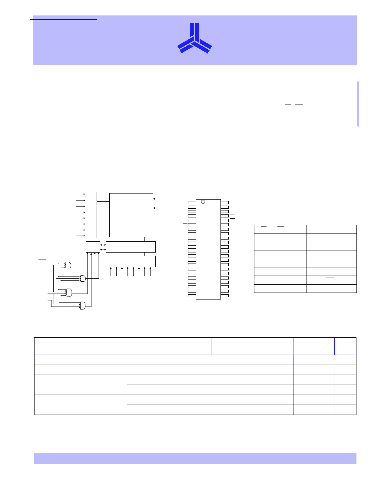
Logic bl ock d ia gr am
A0
A1
WE
UB
OE
LB
CE
A2
A3
A4
A5
A6
A7
I/O0–I/O7
I/O8–I/O15
Row decoder
I/O
buffer
64K × 16
Array
Control circuit
Column decoder
A8
A9
A10
A11
A12
A13
A14
• Low power consumption: STANDBY
- 28 mW (AS7C1026) / max CMOS I/O
- 18 mW (AS7C31026) / max CMOS I/O
• 2.0V data retention
• Easy memory expansion with CE
, OE inputs
• TTL-compatible, three-state I/O
• JEDEC standard packaging
- 44-pin 400 mil SOJ
- 44-pin 400 mil TSOP II
- 48-ball 6 mm × 8 mm CSP mBGA
• ESD protection
• Latch-u p cu rrent
≥ 2000 volts
≥ 200 mA
Pin arrangement
44-Pin SOJ, TSOP II (400 mil)
V
CC
GND
I/O0
I/O1
I/O2
I/O3
GND
I/O4
I/O5
I/O6
I/O7
A15
V
WE
A15
A14
A13
A12
NC
A4
A3
A2
A1
A0
CE
1
2
3
4
5
6
7
8
9
10
11
CC
12
13
14
AS7C102
15
16
17
18
19
20
21
22
A5
44
43
A6
42
A7
41
40
39
38
37
36
35
34
33
32
31
30
29
28
27
26
25
24
23
48-CSP mini Ball-Grid-Array Package
OE
UB
LB
I/O15
I/O14
I/O13
I/O12
GND
V
CC
I/O11
I/O10
I/O9
I/O8
NC
A8
A9
A10
A11
NC
123456
ALB
OE A
BI/O8UB
CI/O9
DV
I/O10
I/O11
SS
EVDDI/O12
FI/O14
I/O13
A14 A15 I/O5 I/O6
A1A
0
A3 A4 CE I/O0
A5 A6 I/O1 I/O2
NC A7 I/O3 V
NC NC I/O4 V
G I/O15 NC A12 A13 WE
HNC A8 A9A10A11NC
NC
2
DD
SS
I/O7
Selection guide
AS7C1026-12
AS7C31026-10
AS7C31026-12
Maximum addre ss access time 10 12 15 20 ns
Maximum output enable access time 5 6 8 10 ns
AS7C1026 – 160 150 140 mA
Maxim u m ope r a ti n g curr e nt
AS7C31026 125 110 100 90 mA
AS7C1026 – 3 3 3 mA
Maximum CMOS standby current
AS7C31026 3 3 3 3 mA
Shaded areas indicate preliminary information.
DID 11-20011-A. 5/22 /0 0 ALLIANCE SEMICONDUCTOR 1
AS7C1026-15
AS7C31026-15
Copyright ©1999 Alliance Semiconductor. All rights reserved.
AS7C1026-20
AS7C31026-20 Unit
SRAM
AS7C1026
AS7C31026
®
Functional descri pti on
The AS7C102 6 and AS7C31026 ar e high-perform ance CMOS 1,048,576 -bit Static Random Access Me mory (S RAM) devices
organized as 65, 536 words x 16 bits. They are desig ne d for memory applic ati on s where fast data ac ce ss, low power, and simple
interfacing are desired.
Equal a ddres s ac ce ss an d cyc l e t i mes ( t
are ideal for high-performance applications.
Whe n CE
is high the device s ente r stanby mo de. The AS7C1 026 is guarant eed not to excee d 28 mW power consumpt ion in
CMOS standby m ode. The devices a lso offe r 2 .0V data retention.
A writ e cycle is acco mplished by ass erting wr ite enable (WE
written on the rising edge of WE
(write cycle 1) or CE (write cycle 2). To avoid bus contention, external devices should drive I/
O pins only after outputs h ave been disabled with output ena ble (OE
A read cycle is accomplished b y asserting output e nable (OE
I/O pins with the data word referenced by the input address. When either chip enable or output enable is inactive, or write
enable is active, ou tp ut driv e rs stay in high-impedance mode.
The devices provide multiple center power and ground pins, and separate byte enable controls, allowing individual bytes to be
written an d re ad . LB
controls the lowe r bit s, I/O0 – I/O7 , a nd UB controls the higher bits, I/O8–I/O15.
All chip inputs and outputs are TTL-compatible, and operation is from a single 5V supply (AS7C1026) or 3.3V supply
(AS7C31026). the device is packaged in common industry standard packages. Chip scale BGA packaging, easy to use in
manufacturing, provides the smallest possible footprint. This 48-ball JEDEC-registered package has a ball pitch of 0.75 mm and
external dimensions of 8 mm × 6 mm.
, tRC, tWC) of 10/12/ 15/20 ns wit h o ut put enable a c ce ss times ( tOE) of 5/6/8 /10 ns
AA
) and chip enable (CE). Data on the input pins I/O0–I/O15 is
) or write enable (WE).
) and chip enable ( CE), with write enable (WE) high. the chips drive
Absolute maximum ratings
Parameter Symbol Min Max Unit
Voltage on V
relative to GND
CC
AS7C31026 V
Voltage on any pin relative to GND V
Pow er dissipation P
Storage temperature (plastic) T
Ambient temperature with VCC applied T
DC current in to out puts (low) I
Note: Str esses greater than those listed unde r A b so l ute Maxi mu m Rating s may cause permanent damage to th e d ev ice. T h is is a stress rating o nly and fun ctional operation of the device at these or any other conditions outside those indicated in the operational sections of this specification is not implied. Exposure
to absolute maximum rating conditions for extended periods may affect reliability.
AS7C1026 V
t1
t1
t2
D
stg
bias
OUT
–0.50 +7.0 V
–0.50 +5.0 V
–0.50 VCC +0.50 V
–1.0W
–65 +150 °C
–55 +125 °C
–20mA
Truth table
CE
H X X X X High Z High Z Standby (I
LHLLHD
LHLHLHigh ZD
LHLLLD
LLXLL D
LLXLHD
WE OE LB UB I/O0–I/O7 I/O8–I/O15 Mode
OUT
OUT
IN
IN
High Z Read I/O0–I/O7 (ICC)
Read I/O8–I/O15 (I
Read I/O0– I/ O15 (ICC)
Write I/O0–I/O15 (ICC)
D
OUT
OUT
D
IN
High Z Write I/O0–I/O7 (ICC)
), I
)
SB
SBI
CC)
2 ALLIANCE SEMICONDUCTOR DID 11-20011- A. 5/22/00
®
CE WE OE LB UB I/O0–I/O7 I/O8–I/O15 Mode
LLXHLHigh ZDINWrite I/O8–I/O15 (ICC)
L
L
Key: H = High, L = Low, X = don’t care.
H
X
H
X
X
H
X
H
High Z High Z Output disable (I
Recommended operating conditions
Parameter Device Symbol Min Typ Max Unit
Supply voltage
Input voltage
Ambient ope ra ting temperatu re
†
VIL min = –3.0V for pulse width less than tRC/2.
AS7C1026 V
AS7C31026 (–1 0) V
AS7C31026 (1 2/ 15/ 20 ) V
AS7C1026 V
AS7C31026 V
commercial T
industrial T
CC
CC
CC
IH
IH
V
IL
A
A
4.5 5.0 5.5 V
3.15 3.3 3.6 V
3.0 3.3 3.6 V
2.2 – VCC + 0.5 V
2.0 – VCC + 0.5 V
†
–0.5
–0.8 V
0– 70 °C
–40 – 85 °C
AS7C1026
AS7C31026
)
CC
SRAM
SRAM
DC operating characteristics (over the operating range)
Parameter Sym Test conditions Device
Input leakage
current
Outp ut leaka ge
current
| ILI |
| ILO |
Operating
power supp ly
I
CC
current
I
Standby
SB
power supp ly
current
Output
voltage
Shaded areas indicate preliminary information.
VCC = Max, CE ≥ VCC–0.2V,
I
SB1
V
OL
V
OHIOH
VCC = Max
= GND to V
V
IN
CC
VCC = Max
= VIH,
CE
= GND to V
V
OUT
VCC = Max, CE ≤ V
CC
IL
AS7C1026 – – – 160 – 150 – 140 mA
outputs op en,
Max
= 1/t
RC
f = f
VCC = Max, CE ≤ VIL,
outputs op en,
Max
= 1/t
RC
f = f
AS7C31026 – 125 – 110 – 100 – 90 mA
AS7C1026 – ––40–40–40
AS7C31026
AS7C1026
≤ GND + 0.2V or
V
IN
≥ VCC–0.2V, f = 0
V
IN
AS7C31026
IOL = 8 mA, VCC = Min – 0.4 – 0.4 – 0.4 – 0.4 V
= –4 mA, VCC = Min 2.4 – 2.4 – 2.4 – 2.4 – V
Capacitance (f = 1MHz, Ta = 25 °C, VCC = NOMINAL)
-10 -12 -15 -20
Min Max Min Max M in Max Min Max
– 1–1–1 –1µA
– 1–1–1 –1µA
– 25 – 25 – 25 – 25
– ––10–10–10
– 10 – 10 – 10 – 10
Unit
mA
mA
Parameter Symbol Signals Test conditions Max Unit
Input capacitance C
I/O capacitance C
DID 11-20011-A. 5/22/00 ALLIANCE SEMICONDUCTOR 3
IN
I/O
A, CE, WE, OE, LB, UB VIN = 0V 5 pF
I/O VIN = V
= 0V 7 pF
OUT
 Loading...