

Page 1

January 2007
512K X 8 BIT LOW POWER CMOS SRAM
OCTOBER 2007
AS6C4008
10/OCTOBER/07, V.1.1
Alliance Memory Inc.
Page 1 of 1
512K X 8 BIT LOW POWER CMOS SRAM
FEATURES
Coming
Soon!
Access time : 55 ns
Low power consumption:
Operatingcurrent : 30/20mA (TYP.)
Standby current : 4µA (TYP.) C-version
Single 2.7V ~ 5.5V power supply
Fully Compatible with all Competitors 5V product
Fully Compatible with all Competitors 3.3V product
Fully static operation
Tri-state output
Data retention voltage : 2.0V (MIN.)
All products ROHS Compliant
Package:32-pin 450 mil SOP
32-pin 8mm x 20mm TSOP-I
32-pin 600 mil P-DIP
:
32-pin 8mm x 13.4mm sTSOP
*36-ball 6mm x 8mm TFBGA
*
GENERAL DESCRIPTION
The AS6C4008 is a 4,194,304-bit low power
CMOS static random access memory organized as
524,288 words by 8 bits. It is fabricated using very
high performance, high reliability CMOS technology.
Its standby current is stable within the range of
operating temperature.
The AS6C4008 is well designed for very low power
system applications, and particularly well suited for
battery back-up non -volatile memory application.
T he AS6C4008 operates from a single power
supply of 2.7V ~ 5.5V
.
FUNCTIONAL BLOCK DIAGRAM
Vcc
Vss
A0-A18
DQ0-DQ7
CE#
WE#
OE#
DECODER
I/O DATA
CIRCUIT
CONTROL
CIRCUIT
512Kx8
MEMORY ARRAY
COLUMN I/O
PIN DESCRIPTION**
SYMBOL DESCRIPTION
A0 - A18 Address Inputs
DQ0 – DQ7 Data Inputs/Outputs
CE# Chip Enable Inputs
WE# Write Enable Input
OE# Output Enable Input
V
CC
V
SS
NC No Connection
Power Supply
Ground
Page 2
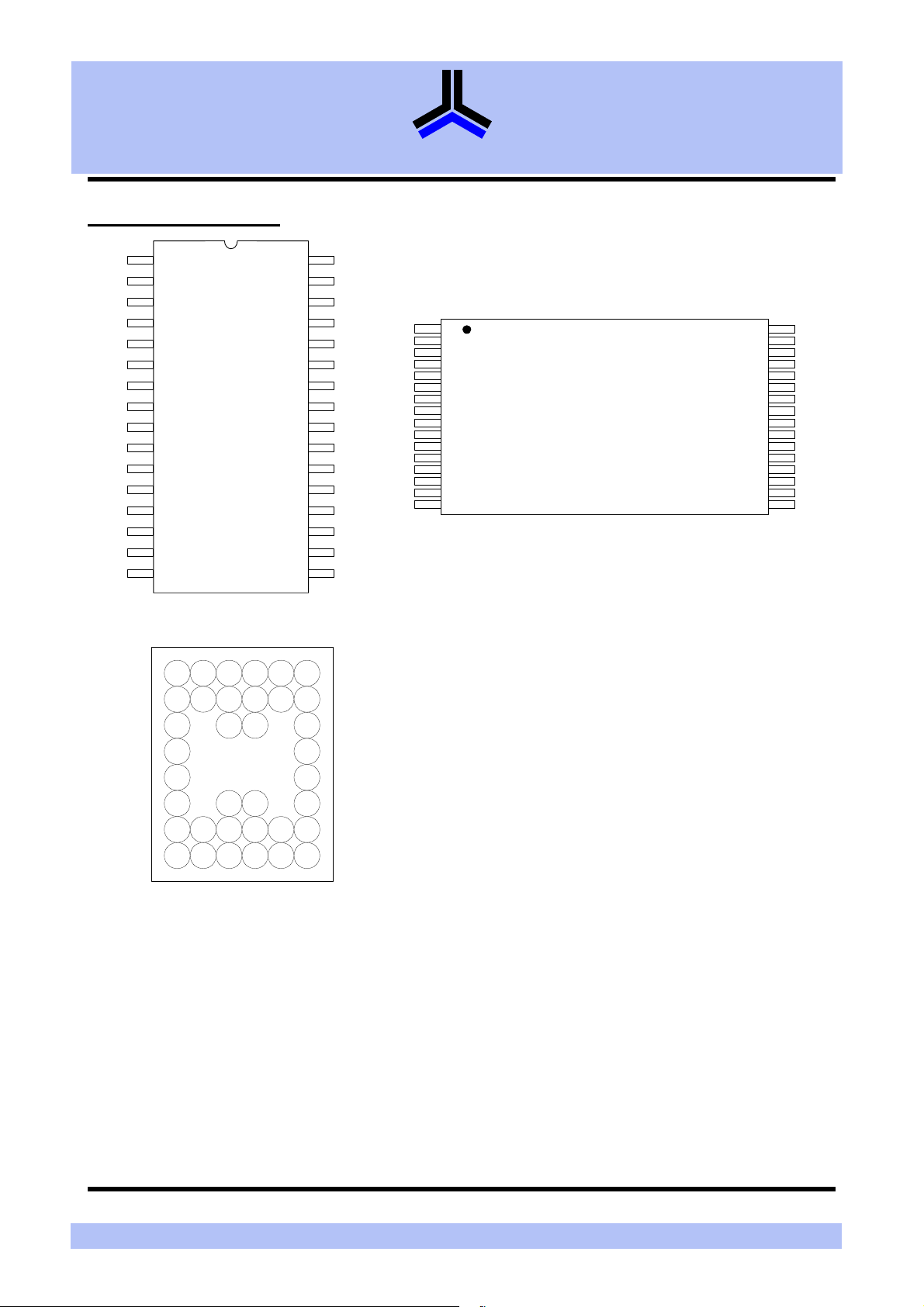
PIN CONFIGURATION
512K X 8 BIT LOW POWER CMOS SRAM
OCTOBER 2007
AS6C4008
10/OCTOBER/07, V.1.1
Alliance Memory Inc.
Page 2 of 15
®
A18
A16
A14
A12
A7
A6
A5
A4
A3
A2
A1
A0
DQ0
DQ1
DQ2
Vss
A8
DQ0
DQ1
Vcc
Vss
DQ2
DQ3
Vcc
A15
A17
WE#
A13
A8
A9
A11
OE#
A10
CE#
DQ7
DQ6
DQ5
DQ4
DQ3
A11
A9
A8
A13
WE#
A17
A15
Vcc
A18
A16
A14
A12
A7
A6
A5
A4 A3
1
2
3
4
5
6
7
8
9
10
11
12
13
14
15
AS6C4008
TSOP-I/sTSOP
32
31
30
29
28
27
26
25
24
23
22
21
20
19
18
1716
OE#
A10
CE#
DQ7
DQ6
DQ5
DQ4
DQ3
Vss
DQ2
DQ1
DQ0
A0
A1
A2
A6A1 A3
A7
A4A2
A5NC
A17
A15
A16
A12A11 A13
32
31
30
29
28
27
26
25
24
23
22
21
20
19
18
1716
1
2
3
4
5
6
7
8
9
10
11
12
13
14
15
A0
A
DQ4
B
DQ5
C
Vss
D
Vcc
E
DQ6
F
DQ7
G
A9
H
AS6C4008
SOP/P-DIP
NC
WE#
A18
OE#
CE#
A10 A14
1 2 3 4 5 6
TFBGA
Page 3

®
512K X 8 BIT LOW POWER CMOS SRAM
OCTOBER 2007
AS6C4008
10/OCTOBER/07, V.1.1
Alliance Memory Inc.
Page 3 of 15
ABSOLUTE MAXIMUM RATINGS*
PARAMETER SYMBOL RATING UNIT
Terminal Voltage with Respect to VSS VTERM -0.5 to 6.5 V
0 to 70(C grade)
TerutarepmeTgnitarepO A
ºC
-40 to 85(I grade)
TerutarepmeTegarotS STG -65 to 150 ºC
PnoitapissiDrewoP D 1 W
ItnerruCtuptuOCD OUT 50 mA
Soldering Temperature (under 10 sec) TSOLDER 260 ºC
*Stresses greater than those listed under “Absolute Maximum Ratings” may cause permanent damage to the device. This is a stress
rating only and functional operation of the device or any other conditions above those indicated in the operational sections of this
specification is not implied. Exposure to the absolute maximum rating conditions for extended period may affect device reliability.
TRUTH TABLE
MODE
Standby
Output Disable
Read
Write
Note: H = VIH, L = VIL, X = Don't care.
CE# OE# WE#
H X X High-Z I
L H H High-Z I
L L H D
L X L D
I/O OPERATION
OUT
IN
SUPPLY CURRENT
DC ELECTRICAL CHARACTERISTICS
PARAMETER
Supply Voltage V
Input High Voltage V
Input Low Voltage V
Input Leakage Current I
Output Leakage
Current
Output High Voltage V
Output Low Voltage V
Average Operating
Power supply Current
SYMBOL TEST CONDITION MIN. TYP.
CC
*1
IH
*1
IL
VCC≧ VIN≧ V
LI
VCC≧ V
I
LO
Output Disabled
OHIOH
OLIOL
Cycle time = Min.
I
CC
CE# = 0.2V, I
SS
≧ VSS,
OUT
= 2mA - - 0.4 V
- 55 -
= 0mA
I/O
V*7.0
CC
- 1 - 1
- 1 - 1
other pins at 0.2V or VCC- 0.2V
Cycle time = 1µs
I
CC1
CE# = 0.2V, I
I/O
= 0mA
-
other pins at 0.2V or VCC- 0.2V
Standby Power
Supply Current
Notes: 1. VIH(max) = VCC+ 3.0V for pulse width less than 10ns. VIL(min) = VSS- 3.0V for pulse width less than 10ns.
2. Over/Undershoot specifications are characterized, not 100% tested.
3. Typical values are included for reference only and are not guaranteed or tested.
Typical valued are measured at VCC= VCC(TYP.) and TA= 25ºC
4. 25µA for special request
*C=Commercial temperature/I = Industrial temperature
I
SB1
CE# V≧CC- 0.2V
*C 4 50
*I
-
-
*3
MAX. UNIT
- VCC+0.3 V
30 60
4
4 50
SB1
CC,ICC1
ICC,I
CC1
ICC,I
CC1
10 mA
*4
*4
V5.50.37.2
V6.0-2.0-
µ
µ
V--4.2Am1-=
mA
µ
µ
A
A
A
A
Page 4
®
512K X 8 BIT LOW POWER CMOS SRAM
OCTOBER 2007
AS6C4008
10/OCTOBER/07, V.1.1
Alliance Memory Inc.
Page 4 of 15
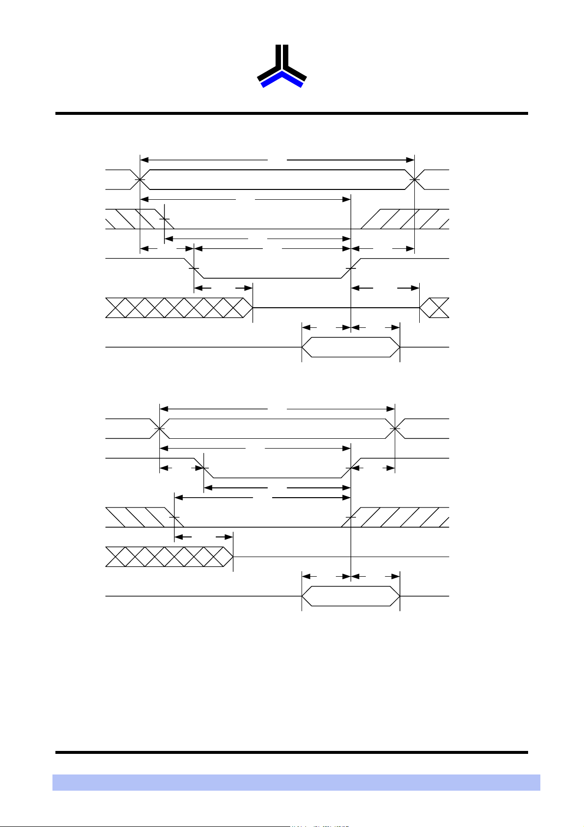
WRITE CYCLE 1 (WE# Controlled) (1,2,3,5,6)
Address
tAW
CE#
WE#
tWHZ
Dout
Din
(4)
WRITE CYCLE 2 (CE# Controlled) (1,2,5,6)
tCW
tWP
tWC
High-Z
tDW tDH
Data Valid
tWRtAS
TOW
(4)
tWC
Address
tAW
CE# tWRtAS
tCW
tWP
WE#
tWHZ
Dout
Din
Notes :
1.WE#, CE# must be high during all address transitions.
2.A write occurs during the overlap of a low CE#, low WE#.
3.During a WE# controlled write cycle with OE# low, t
placed on the bus.
4.During this period, I/O pins are in the output state, and input signals must not be applied.
5.If the CE# low transition occurs simultaneously with or after WE# low transition, the outputs remain in a high impedance state.
6.t
OW
and t
are specified with CL = 5pF. Transition is measured ±500mV from steady state.
WHZ
(4)
must be greater than t
WP
High-Z
tDW tDH
Data Valid
+ tDW to allow the drivers to turn off and data to be
WHZ
Page 5
AS6C4008
10 October 2007, v 1.1
Alliance Memory Inc.,
OCTOBER 2007
Rev. 1.1
Notes:
1. V
2. V
3. Over/Undershoot specifications are characterized, not 100% tested.
4. Typical values are included for reference only and are not guaranteed or tested.
Typical valued are measured at V
(max) = V
IH
(min) = V
IL
+ 3.0V for pulse width less than 10ns.
CC
- 3.0V for pulse width less than 10ns.
SS
512K X 8 BIT LOW POWER CMOS SRAM
= VCC(TYP.) and TA= 25
CC
?
CAPACITANCE (TA = 25 , f℃ = 1.0MHz)
PARAMETER SYMBOL MIN. MAX UNIT
C ecnaticapaC tupnI
IN
Input/Output Capacitance C
Note : These parameters are guaranteed by device characterization, but not production tested.
I/O
-
-
AC TEST CONDITIONS
V ot V2.0 sleveL esluP tupnI
- 0.2V
CC
sn3 semiT llaF dna esiR tupnI
Input and Output Timing Reference Levels 1.5V
C daoL tuptuO
= 30pF + 1TTL, IOH/IOL = -1mA/2mA
L
AC ELECTRICAL CHARACTERISTICS
6 pF
8 pF
(1) READ CYCLE
PARAMETER SYM.
AS6C4008-55
UNIT
MIN. MAX. MIN. MAX. MIN. MAX.
Read Cycle Time tRC 55 - ns
Address Access Time tAA - 55 ns
Chip Enable Access Time t
- 55 ns
ACE
Output Enable Access Time tOE - 30 ns
Chip Enable to Output in Low-Z t
Output Enable to Output in Low-Z t
Chip Disable to Output in High-Z t
Output Disable to Output in High-Z t
* 10 - ns
CLZ
* 5 - ns
OLZ
* - 20 ns
CHZ
* - 20 ns
OHZ
Output Hold from Address Change tOH 10 - ns
(2) WRITE CYCLE
PARAMETER SYM.
AS6C4008-55
UNIT
MIN. MAX. MIN. MAX. MIN. MAX.
Write Cycle Time tWC 55 - ns
Address Valid to End of Write tAW 50 - ns
Chip Enable to End of Write tCW 50 - ns
Address Set-up Time tAS 0 - ns
Write Pulse Width tWP 45 - ns
Write Recovery Time tWR 0 - ns
Data to Write Time Overlap tDW 25 - ns
Data Hold from End of Write Time tDH 0 - ns
Output Active from End of Write tOW* 5 - ns
Write to Output in High-Z t
*These parameters are guaranteed by device characterization, but not production tested.
* - 20 ns
WHZ
Page 5 of 15
Page 6

®
512K X 8 BIT LOW POWER CMOS SRAM
OCTOBER 2007
AS6C4008
10/OCTOBER/07, V.1.1
Alliance Memory Inc.
Page 6 of 15
TIMING WAVEFORMS
READ CYCLE 1 (Address Controlled) (1,2)
tRC
Address
Dout Data Valid
READ CYCLE 2 (CE# and OE# Controlled) (1,3,4,5)
Address
CE#
Previous Data Valid
tRC
tAA
tOHtAA
tACE
OE#
tOE
tOLZ
tCLZ
tOH
tOHZ
tCHZ
Dout Data Valid
Notes :
1.WE#
is high for read cycle.
2.Device is continuously selected OE# = low, CE# = low
3.Address must be valid prior to or coincident with CE# = low,; otherwise tAA is the limiting parameter.
4.t
, t
, t
CLZ
OLZ
5.At any given temperature and voltage condition, t
CHZ
and t
are specified with CL= 5pF. Transition is measured ±500mV from steady state.
OHZ
.
is less than t
CHZ
CLZ
, t
is less than t
OHZ
OLZ.
High-ZHigh-Z
Page 7

®
512K X 8 BIT LOW POWER CMOS SRAM
OCTOBER 2007
AS6C4008
10/OCTOBER/07, V.1.1
Alliance Memory Inc.
Page 7 of 15
WRITE CYCLE 1 (WE# Controlled) (1,2,3,5,6)
Address
tAW
CE#
WE#
tWHZ
Dout
Din
(4)
WRITE CYCLE 2 (CE# Controlled) (1,2,5,6)
tCW
tWP
tWC
High-Z
tDW tDH
Data Valid
tWRtAS
TOW
(4)
tWC
Address
tAW
CE# tWRtAS
tCW
tWP
WE#
tWHZ
Dout
Din
Notes :
1.WE#, CE# must be high during all address transitions.
2.A write occurs during the overlap of a low CE#, low WE#.
3.During a WE# controlled write cycle with OE# low, t
placed on the bus.
4.During this period, I/O pins are in the output state, and input signals must not be applied.
5.If the CE# low transition occurs simultaneously with or after WE# low transition, the outputs remain in a high impedance state.
6.t
OW
and t
are specified with CL = 5pF. Transition is measured ±500mV from steady state.
WHZ
(4)
must be greater than t
WP
High-Z
tDW tDH
Data Valid
+ tDW to allow the drivers to turn off and data to be
WHZ
Page 8

®
512K X 8 BIT LOW POWER CMOS SRAM
OCTOBER 2007
AS6C4008
10/OCTOBER/07, V.1.1
Alliance Memory Inc.
Page 8 of 15
DATA RETENTION CHARACTERISTICS
PARAMETER SYMBOL TEST CONDITION MIN. TYP. MAX. UNIT
VCCfor Data Retention V
I
Data Retention Current
Chip Disable to Data
Retention Time
DR
t
Recovery Time t
t
= Read Cycle Time **C=Commercial temperature/I=Industrial temperature
RC
*
CE# V≧
DR
V
= 2.0V
CC
CE# V≧
See Data Retention
CDR
Waveforms (below)
R
- 0.2V 2.0 - 5.5 V
CC
CC
- 0.2V
**C
**I - 2 30
- 2 30
0 - - ns
t
RC
*
- - ns
DATA RETENTION WAVEFORM
VDR ≧ 2.0V
µ
A
µ
Vcc
CE#
Vcc(min.)
V
IH
CE# V≧ cc-0.2V
Vcc(min.)
tRtCDR
VIH
Page 9

®
512K X 8 BIT LOW POWER CMOS SRAM
OCTOBER 2007
AS6C4008
10/OCTOBER/07, V.1.1
Alliance Memory Inc.
Page 9 of 1
PACKAGE OUTLINE DIMENSION
32 pin 450 mil SOP Package Outline Dimension
SYM.
A
A1
A2
b
c
D
E
E1
e
L
L1
S
y
Θ
UNIT
INCH.(BASE) MM(REF)
0.118 (MAX) 2.997 (MAX)
0.004(MIN) 0.102(MIN)
0.111(MAX) 2.82(MAX)
0.016(TYP) 0.406(TYP)
0.008(TYP) 0.203(TYP)
0.817(MAX) 20.75(MAX)
0.445±0.005 11.303 ±0.127
0.555±0.012 14.097 ±0.305
0.050(TYP) 1.270(TYP)
0.0347±0.008 0.881 ±0.203
0.055±0.008 1.397 ±0.203
0.026(MAX) 0.660 (MAX)
0.004(MAX) 0.101(MAX)
0o -10o 0o -10
o
Page 10

®
512K X 8 BIT LOW POWER CMOS SRAM
OCTOBER 2007
AS6C4008
10/OCTOBER/07, V.1.1
Alliance Memory Inc.
Page 10 of 15
32 pin 8mm x 20mm TSOP-I Package Outline Dimension
SYM.
A
A1
A2
b
c
D
E
e
HD
L
L1
y
Θ
UNIT
INCH(BASE) MM(REF)
0.047 (MAX) 1.20 (MAX)
0.004±0.002 0.10 ±0.05
0.039±0.002 1.00 ±0.05
0.008 + 0.002
- 0.001
0.20 + 0.05
-0.03
0.005 (TYP) 0.127 (TYP)
0.724±0.004 18.40 ±0.10
0.315±0.004 8.00 ±0.10
0.020 (TYP) 0.50 (TYP)
0.787±0.008 20.00 ±0.20
0.0197±0.004 0.50 ±0.10
0.0315±0.004 0.08 ±0.10
0.003 (MAX) 0.076 (MAX)
o
~
0
o
0
5
o
~
o
5
Page 11

®
512K X 8 BIT LOW POWER CMOS SRAM
OCTOBER 2007
AS6C4008
10/OCTOBER/07, V.1.1
Alliance Memory Inc.
Page 11 of 15
32 pin 8mm x 13.4mm sTSOP Package Outline Dimension
HD
c
L
1
16
32
17
"A"
D
12° (2x)12° (2x)
e
b
Seating Plane
E
y
12° (2X)
16
1
A
A1
A2
b
c
D
E
e
HD
L
L1
y
Θ
UNIT
0.049 (MAX) 1.25 (MAX)
0.005±0.002 0.130 ±0.05
0.039±0.002 1.00 ±0.05
0.008±0.01 0.20±0.025
0.005 (TYP) 0.127 (TYP)
0.465±0.004 11.80 ±0.10
0.315±0.004 8.00 ±0.10
0.020 (TYP) 0.50 (TYP)
0.528±0.008 13.40 ±0.20.
0.0197±0.004 0.50 ±0.10
0.0315±0.004 0.8 ±0.10
0.003 (MAX) 0.076 (MAX)
0
SYM.
17
c
A2A1
A
SEATING PLANE
"A" DETAIL VIEW
32
INCH(BASE) MM(REF)
o
o
~
0
5
o
o
~
5
12° (2X)
GAUGE PLANE
0.254
0
L
L1
Page 12

36 ball 6mm × 8mm TFBGA Package Outline Dimension
512K X 8 BIT LOW POWER CMOS SRAM
Page 12 of 15
®
Page 13

32 pin 600 mil P-DIP Package Outline Dimension
Note : D/E1/S dimension do not include mold flash.
UNIT
SYM.
INCH(BASE) MM(REF)
A1
0.001 (MIN) 0.254 (MIN)
A2
0.150± 0.005 3.810 ± 0.127
B
0.018± 0.005 0.457 ± 0.127
D
1.650± 0.005 41.910 ± 0.127
E
0.600± 0.010 15.240 ± 0.254
E1
0.544± 0.004 13.818 ± 0.102
e
0.100 (TYP) 2.540 (TYP)
eB
0.640± 0.020 16.256 ± 0.508.
L
0.130± 0.010 3.302 ± 0.254
S
0.075± 0.010 1.905 ± 0.254
Q1
0.070± 0.005 1.778 ± 0.127
512K X 8 BIT LOW POWER CMOS SRAM
Page 13 of 15
®
Page 14

ORDERING INFORMATION
AS6C 4008 - 55 X X N
Temperature Range:
C = Commercial
(0ºC to +70º C)
I = Industrial
(-40º to +85º C)
N = Lead
Free ROHS
Compliant
Part
low
power
SRAM
prefix
Device
Number
40 = 4M
08 = by 8
Access
Time
Ordering Codes
512K X 8 BIT LOW POWER CMOS SRAM
OCTOBER 2007
AS6C4008
10/OCTOBER/07, V.1.1
Alliance Memory Inc.
®
Alliance Organization VCC range Package
AS6C4008-55PCN
AS6C4008-55SIN
AS6C4008-55TIN
AS6C4008-55STIN
AS6C4008-55BIN
512k x 8 2.7-5.5V 32pin 600mil PDIP
512k x 8 2.7-5.5V 32pin 450mil SOP
512k x 8 2.7-5.5V 32pin TSOP-I (8 x 20 mm)
512k x 8 2.7-5.5V 32pin sTSOP (8 x 13.4 mm)
512k x 8 2.7-5.5V
Part numbering system
36pin TFBGA (6mm x 8mm)
*Coming Soon!
*
Operating
Temp
Commercial ~
0º C to 70º C
Industrial ~
-40ºC to 85º C
Industrial ~
-40ºC to 85º C
Industrial ~
-40ºC to 85º C
Industrial ~
-40ºC to 85º C
Speed
ns
55
55
55
55
55
Package Options:
P = 32 pin 600 mil P-DIP
S = 32 pin 450 mil SOP
T = 32 pin TSOP-I (8mm x 20 mm)
ST = 32 pin sTSOP (8mm x 13.4 mm)
B=36 pin TFBGA (6mm x 8mm)*
* Coming Soon!
Page 14 of 15
Page 15

®
®
Page 15 of 15
Alliance Memory, Inc.
1116 South Amphlett, #2,
San Mateo, CA 94402
Tel: 650-525-3737
Fax: 650-525-0449
Copyright © Alliance Memory
All Rights Reserved
Part Number: AS6C4008
Document Version: v. 1.
1
www.alliancememory.com
© Copyright 2003 Alliance Memory, Inc. All rights reserved. Our three-point logo, our name and Intelliwatt are trademarks or registered trademarks of
Alliance. All other brand and product names may be the trademarks of their respective companies. Alliance reserves the right to make changes to this
document and its products at any time without notice. Alliance assumes no responsibility for any errors that may appear in this document. The data
contained herein represents Alliance's best data and/or estimates at the time of issuance. Alliance reserves the right to change or correct this data at any
time, without notice. If the product described herein is under development, significant changes to these specifications are possible. The information in
this product data sheet is intended to be general descriptive information for potential customers and users, and is not intended to operate as, or provide,
any guarantee or warrantee to any user or customer. Alliance does not assume any responsibility or liability arising out of the application or use of any
product described herein, and disclaims any express or implied warranties related to the sale and/or use of Alliance products including liability or
warranties related to fitness for a particular purpose, merchantability, or infringement of any intellectual property rights, except as express agreed to in
Alliance's Terms and Conditions of Sale (which are available from Alliance). All sales of Alliance products are made exclusively according to Alliance's
Terms and Conditions of Sale. The purchase of products from Alliance does not convey a license under any patent rights, copyrights; mask works rights,
trademarks, or any other intellectual property rights of Alliance or third parties. Alliance does not authorize its products for use as critical components in
life-supporting systems where a malfunction or failure may reasonably be expected to result in significant injury to the user, and the inclusion of
Alliance products in such life-supporting systems implies that the manufacturer assumes all risk of such use and agrees to indemnify Alliance against all
claims arising from such use.
 Loading...