

Alliance MEMORY AS6C1008 Service Manual
February 2007
128K X 8 BIT LOW POWER CMOS SRAM
AS6C1008
02/February/07, v 1.0
Alliance Memory Inc.
Page 1 of 14
®
FEATURES
Access tim e :55ns
Low powe r consumption:
Operating current:10 mA (TYP.)
Standby current: 1 µA (TYP.)
Single 2.7V ~ 5.5V po we r supply
Fully Compatible with all Competitors 5V product
Fully Compatible with all Competitors 3.3V product
Fully static operation
Tri-state output
Data retention voltage : 1.5V (MIN.)
All products are ROHS Compliant
Package : 32-pin 450 mil SOP
32-pin 600 mil P-DIP
32-pin 8mm x 20mm TSOP-I
32-pin 8mm x 13.4mm sTSOP
36-ball 6mm x 8mm TFBGA
GENERA L DESCRIPTION
The AS6C1008 is a 1,048,57 6-bit low powe r
CMOS static rand om access memory organized as
131,072 words by 8 bits. It is fabricated using ve ry
high performance, high reliability CMO S technolo gy. Its
standby current is stable within the ra nge of
operating temperature.
The AS6C1008 is well designed for very low power
system applications, and part icula rly well suited for
battery back-up non-volatile memory a pplication.
The AS6C1008 operates from a single power supply
of 2.7V ~ 5.5V.
.
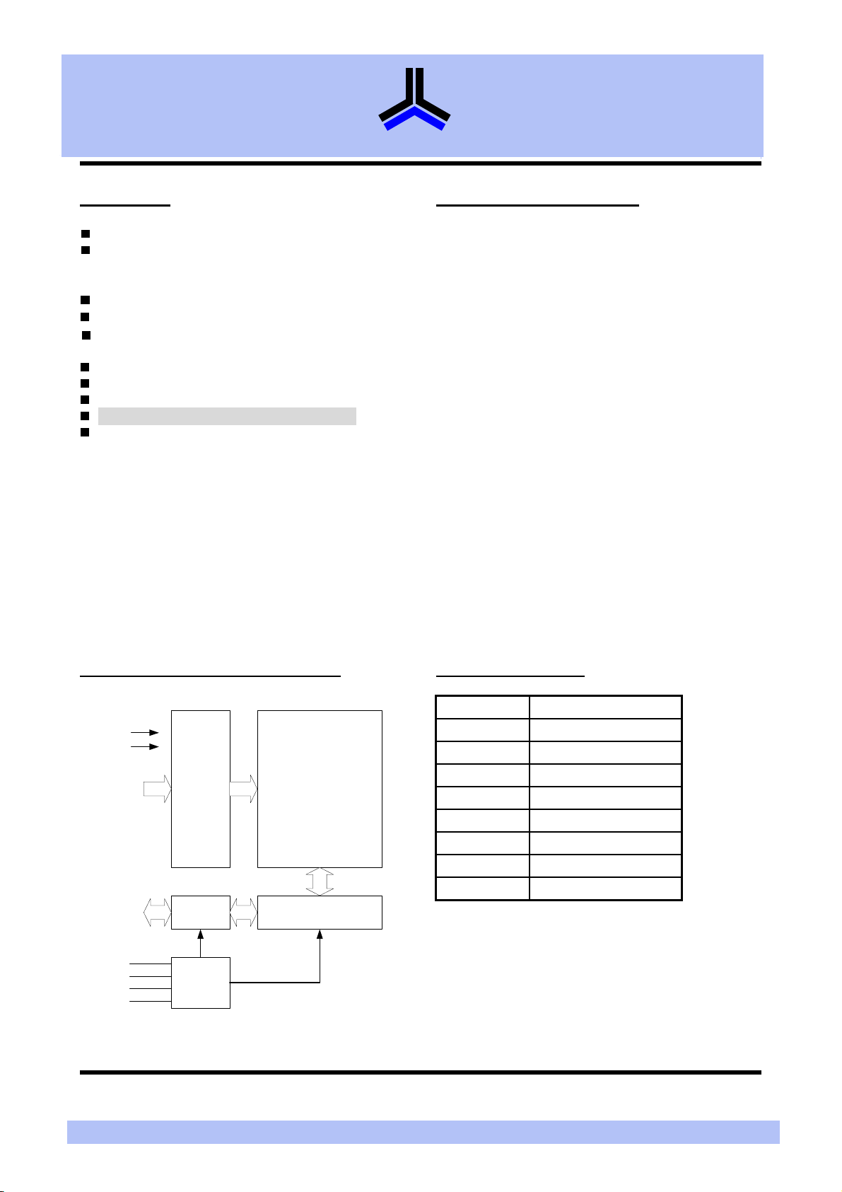
FUNCTIONAL BLOCK DIAGRAM
Vcc
Vss
A0-A16
DQ0-DQ7
CE#
CE2
WE#
OE#
DECODER
I/O DATA
CIRCUIT
CONTROL
CIRCUIT
128Kx8
MEMORY ARRAY
COLUMN I/O
PIN DESCRIPTION
SYMBOL DESCRIPTION
A0 - A16 Address Inputs
DQ0 – DQ7 Data Inputs/Outputs
CE#, CE2 Chip Enable Inputs
WE# Write Enable Input
OE# Output Enable Input
V
C C
V
SS
NC No C onnection
Power Supply
Ground

February 2007
128K X 8 BIT LOW POWER CMOS SRAM
AS6C1008
02/February/07, v 1.0
Alliance Memory Inc.
Page 2 of 14
PIN CONFIGURATION
®
NC
A16
A14
A12
A7
A6
A5
A4
A3
A2
A1
A0
DQ0
DQ1
DQ2
Vss
Vcc
A15
CE2
WE#
A13
A8
A9
A11
OE#
A10
CE#
DQ7
DQ6
DQ5
DQ4
DQ3
A11
A9
A8
A13
WE #
CE 2
A15
Vc c
NC
A16
A14
A12
A7
A6
A5
A4 A3
1
2
3
4
5
6
7
8
9
10
11
12
13
14
15
AS6C1008
TS OP -I/sTSOP
32
31
30
29
28
27
26
25
24
23
22
21
20
19
18
1716
OE #
A10
CE #
DQ 7
DQ 6
DQ 5
DQ 4
DQ 3
Vss
DQ 2
DQ 1
DQ 0
A0
A1
A2
A6A1 A3
A7
A15
32
31
30
29
28
27
26
25
24
23
22
21
20
19
18
1716
A8
DQ0
DQ1
Vcc
Vss
DQ2
DQ3
31A11A 21A
1
2
3
4
5
6
7
8
9
10
11
12
13
14
15
A0
A
DQ4
B
DQ5
C
Vss
D
Vcc
E
DQ6
F
DQ7
G
A9
H
AS6C1008
SOP/P-DIP
CE2
WE#
A4A2
CN 5A
NC
NC
OE#
CE#
A16
A10 A14
1 2 3 4 5 6
TFBGA
.
®
February 2007
128K X 8 BIT LOW POWER CMOS SRAM
AS6C1008
02/February/07, v 1.0
Alliance Memory Inc.
Page 3 of 14
ABSOLUTE MAXIMUM RATINGS*
PARAMETER SYMBOL RATING UNIT
Terminal Voltage with Respect to VSS VTERM -0.5 to 7.0 V
0 to 70(C grade)
T erutarepmeT gnitarepO A
ºC
-40 to 85(I grade)
T erutarepmeT egarotS STG -65 to 150
ºC
P noitapissiD rewoP D 1 W
I tnerruC tuptuO CD OUT 50 mA
Soldering Temperature (under 10 sec) TSOLDER 260 ºC
*Stresses greater than those listed under “Absolute Maximum Ratings” may cause permanent damage to the device. This is a stress
rating only and functional operation of the device or any other conditions above those indicated in the operational sections of this
specification is not implied. Exposure to the absolute maximum rating conditions for extended period may affect device reliability.
TRUTH TABLE
MODE
Standby
Output Disable
Read
Write
Note: H = VIH, L = VIL, X = Don't care.
CE# CE2 OE# WE#
H X X X
X L X X
L H H H
L H L H
L H X L
DC ELECTRICAL CHARACTERISTICS
PARAMETER
Supply Voltage V
Input High Voltage V
Input Low Voltage V
Input Leakage Current I
Output Leakage
Current
Output High Voltage VOH I
Output Low Voltage VOL I
Average Operating
Power supply Current
Standby Power
Supply Current
*C=Commercial temperature/I= Industrial temperature
SYMBOL TEST CONDITION MIN. TYP.
CC
*1
IH
*2
IL
VCC≧ V
LI
V
I
LO
CC
Output Disabled
OH
OL
= 2mA - - 0.4 V
≧ V
IN
OUT
≧ V
≧ V
Cycle time = Min.
I
CC
CE# = V
= 0mA
I
I/O
and CE2 = VIH,
IL
Cycle time = 1µs
≦
CE#
I
CC1
0.2V and CE2≧VCC-0.2V,
= 0mA
I
I/O
other pins at 0.2V or V
I
CE# V≧
SB1
or CE2≦0.2V
-0.2V
CC
SS
I/O OPERATION
High-Z I
High-Z I
High-Z ICC,I
D
ICC,I
OUT
DIN ICC,I
- 1 - 1
SS,
- 55 -
- 1 - 1
10 60
- 1 10 mA
-0.2V
CC
C*
- 1 20
I* - 1 50
SUPPLY CURRENT
SB1
SB1
CC1
CC1
CC1
*4
MAX. UNIT
V -ccV*7.0
+0.3 V
CC
µ
µ
mA
µ
µ
V 5.5 0.3 7.2
V 6.0 - 2.0 -
A
A
V - 7.2 2.2 Am1- =
A
A

®
February 2007
128K X 8 BIT LOW POWER CMOS SRAM
AS6C1008
02/February/07, v 1.0
Alliance Memory Inc.
Page 4 of 14
Notes:
1. V
(max) = VCC+ 3.0V for pulse width less than 10ns.
IH
2. V
(min) = VSS- 3.0V for pulse width less than 10ns.
IL
3. Over/Undershoot specifications are characterized, not 100% tested.
4. Typical values are included for reference only and are not guaranteed or tested.
Typical valued are measured at V
= VCC(TYP.) and TA= 25
CC
ºC
CAPACITANCE (TA = 25 , f℃ = 1.0MHz)
PARAMETER SYMBOL MIN. MAX UNIT
CecnaticapaCtupnI
IN
Input/Output Capacitance C
Note : These parameters are guaranteed by device characterization, but not production tested.
I/O
-
-
AC TEST CONDITIONS
VotV2.0sleveLesluPtupnI
- 0.2V
CC
sn3semiTllaFdnaesiRtupnI
Input and Output Timing Reference Levels 1.5V
CdaoLtuptuO
=30pF + 1TTL, I
L
OH/IOL
6 pF
8 pF
= -1mA/2mA
AC ELECTRICAL CHARACTERISTICS
(1) READ CYCLE
PARAMETER SYM.
AS6C1008-55
MIN. MAX.
Read Cycle Time t
Address Access Time t
Chip Enable Access Time t
Output Enable Access Time t
Chip Enable to Output in Low-Z t
Output Enable to Output in Low-Z t
Chip Disable to Output in High-Z t
Output Disable to Output in High-Z t
Output Hold from Address Change t
RC
AA
ACE
OE
* 10 - ns
CLZ
* 5 - ns
OLZ
* - 20 ns
CHZ
* - 20 ns
OHZ
OH
55 - ns
- 55 ns
- 55 ns
- 30 ns
10 - ns
(2) WRITE CYCLE
PARAMETER SYM.
AS6C1008-55
MIN. MAX.
Write Cycle Time t
Address Valid to End of Write t
Chip Enable to End of Write t
Address Set-up Time t
Write Pulse Width t
Write Recovery Time t
Data to Write Time Overlap t
Data Hold from End of Write Time t
WC
AW
CW
AS
WP
WR
DW
DH
55 - ns
50 - ns
50 - ns
0 - ns
45 - ns
0 - ns
25 - ns
0 - ns
Output Active from End of Write tOW* 5 - ns
Write to Output in High-Z t
*These parameters are guaranteed by device characterization, but not production tested.
* - 20 ns
WHZ
UNIT
UNIT

February 2007
128K X 8 BIT LOW POWER CMOS SRAM
AS6C1008
02/February/07, v 1.0
Alliance Memory Inc.
Page 5 of 14
TIMING WAVEFORMS
READ CYCLE 1 (Address Controlled) (1,2)
tRC
Address
®
tOHtAA
Dout Data Valid
Previous Data Valid
READ CYCLE 2 (CE# and CE2 and OE# Controlled) (1,3,4,5)
tRC
Address
tAA
CE#
ACE
t
CE2
OE#
tOE
tOLZ
tCLZ
Dout Data Valid
tOH
tOHZ
tCHZ
High-ZHigh-Z
Notes :
1.WE# is high for read cycle.
2.Device is continuously selected OE# = low, CE# = low
3.Address must be valid prior to or coincident with CE# = low,CE2 = high; otherwise tAA is the limiting parameter.
4.t
, t
, t
CLZ
OLZ
5.At any given temperature and voltage condition, t
CHZ
and t
are specified with CL= 5pF. Transition is measured ±500mV from steady state.
OHZ
.,
is less than t
CHZ
CE2 = high
.
CLZ
, t
is less than t
OHZ
OLZ.
 Loading...