

Allegro UGN3055U Datasheet
3055
MULTIPLEXED
TWO-WIRE HALL EFFECT
SENSOR IC
3055
Data Sheet
27680
DISCONTINUED PRODUCT
Shown for Reference Only
X
LOGIC
1
BUS
32
GROUND
SWITCH IN
Dwg. PH-005
MULTIPLEXED TWO-WIRE
HALL-EFFECT SENSOR ICs
The UGN3055U Hall-effect sensor is a digital magnetic sensing IC
capable of communicating over a two-wire power/signal bus. Using a
sequential addressing scheme, the device responds to a signal on the
bus and returns the diagnostic status of the IC, as well as the status of
each monitored external magnetic field. As many as 30 sensors can
function on the same two-wire bus. This IC is ideal for multiple sensor
applications where minimizing the wiring harness size is desirable or
essential.
The device consists of high-resolution bipolar Hall-effect switching
circuitry, the output of which drives high-density CMOS logic stages.
These logic stages decode the address pulse and enable a response
at the appropriate address. The combination of magnetic-field or
switch-status sensing, low-noise amplification of the Hall-transducer
output, and high-density decoding and control logic is made possible
by the development of a new sensor BiMOS fabrication technology.
This unique magnetic sensing IC operates within specifications
between -20°C and +85°C. Alternate magnetic and temperature
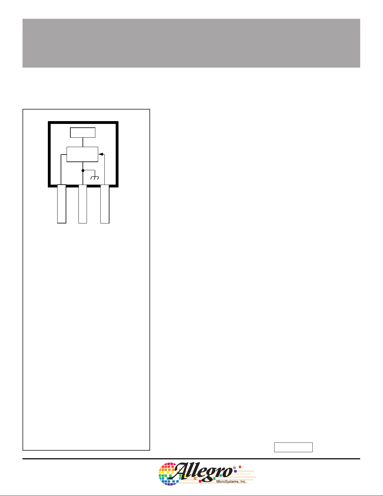
specifications are available upon request. It is supplied in a 60 mil
(1.54 mm) thick, three-pin plastic SIP. Each package is clearly marked
with a two-digit decimal device address (xx).
Pinning is shown viewed from branded side.
ABSOLUTE MAXIMUM RATINGS
at T
= +25°C
A
Supply Voltage, V
Magnetic Flux Density, B............ Unlimited
Operating Temperature Range,
T
.......................... -20°C to +85°C
A
Storage Temperature Range,
.............................. -55°C to +150°C
T
S
Package Power Dissipation,
P
.................................... 750 mW
D
........................... 24 V
BUS
FEATURES
■ Complete Multiplexed Hall-Effect IC with
Simple Sequential Addressing Protocol
■ Allows Power and Communication Over a
Two-Wire Bus (Supply/Signal and Ground)
■ Up to 30 Hall-Effect Sensors Can Share a Bus
■ Sensor Diagnostic Capabilities
■ Magnetic-Field or Switch-Status Sensing
■ Low Power of BiMOS Technology Favors
Battery-Powered and Mobile Applications
■ Ideal for Automotive, Consumer, and Industrial Applications
Always order by complete part number: UGN3055U .

3055
MULTIPLEXED
TWO-WIRE HALL EFFECT
SENSOR IC
OPERATIONAL CHARACTERISTIC over operating temperature range.
Electrical Limits
Characteristics
Power Supply Voltage V
Signal Current I
Quiescent Current V
= 6 V I
BUS
= 9 V I
V
BUS
I
QH–IQL
Address Range Addr 1 — 30 —
Clock Thresholds LOW to HIGH V
HIGH to LOW V
Hysteresis V
Clock Period t
Address LOW Voltage V
Address HIGH Voltage V
Power-On Reset Voltage V
Settling Time V
= 9 V t
BUS
= 6 V t
V
BUS
Propagation Delay LOW to HIGH t
HIGH to LOW t
Pin 3 Input Resistance No Magnetic Field (V
Mag. Field Present (V
= HIGH) R
OUT
= LOW) R
OUT
Magnetic Characteristics
Magnetic Thresholds *Turn-On B
Turn-Off B
Hysteresis (B
*Alternate magnetic switch point specifications are available on request. Please contact the factory.
)B
OP–BRP
Symbol Min. Typ. Max. Units
BUS
S
QH
QL
I
Q
CLH
CHL
CHYS
CLK
L
H
RST
h
l
plh
phl
OUTH
OUTL
OP
RP
HYS
——15V
12 15 20 mA
— — 2.5 mA
— — 2.5 mA
— — 300 µA
— — 8.5 V
6.5 — — V
— 0.8 — V
0.1 1.0 — ms
V
RST
V
CLH
6V
9V
CHL
BUS
2.5 3.5 5.5 V
100 — — µs
100 — — µs
10 — — µs
——10µs
40 — 75 kΩ
——50Ω
50 150 300 G
-25 100 300 G
05075G
V
V
115 Northeast Cutoff, Box 15036
Worcester, Massachusetts 01615-0036 (508) 853-5000
W
Copyright © 1988, 1991, Allegro MicroSystems, Inc.
3055
A
MULTIPLEXED
TWO-WIRE HALL EFFECT
SENSOR IC
(±0.005” [0.13 mm] die placement)
ACTIVE AREA DEPTH
0.015"
0.38 mm
NOM
0.071"
1.80 mm
0.084"
2.13 mm
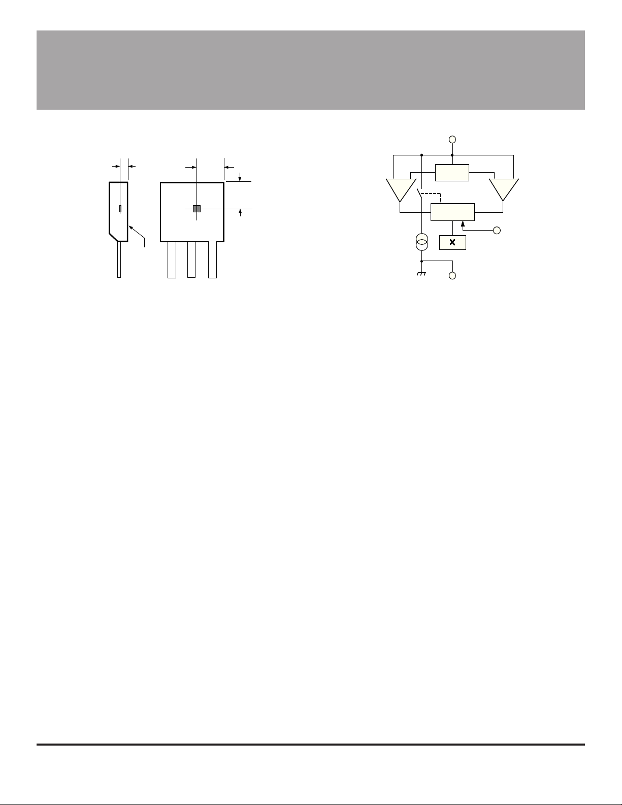
FUNCTIONAL BLOCK DIAGRAMSENSOR LOCATION
1
BUS
REG
COMP COMP
CLOCK
CMOS LOGIC
RESET
SWITCH IN
3
(OPTIONAL)
BRANDED
SURFACE
1 32
Dwg. MH-002A
DEFINITION OF TERMS
Sensor Address
Each bus sensor has a factory-specified predefined
address. At present, allowable sensor addresses are
integers from 1 to 30.
LOW-to-HlGH Clock Threshold (V
Minimum voltage required during the positive-going
transition to increment the bus address and trigger a
diagnostic response from the bus sensors. This is also
the maximum threshold of the on-chip comparator, which
monitors the supply voltage, V
BUS
HlGH-to-LOW Threshold (VHL)
Maximum voltage required during the negative-going
transition to trigger a
signal
current response from the bus
sensors. This is also the maximum threshold of the onchip comparator, which monitors the supply voltage, V
Bus HIGH Voltage (VH)
Bus HIGH voltage required for addressing. Voltage
should be greater than V
CLH
.
Address LOW Voltage (VL)
Bus LOW Voltage required for addressing. Voltage
should be greater than V
Bus Reset Voltage (V
and less than V
RST
)
RST
Voltage level required to reset individual sensors.
Sensor Quiescent Current Drain (IQ)
The current drain of bus sensors when active but not
addressed. IQH is the maximum quiescent current drain
when the sensor is not addressed and is at VH. IQL is the
maximum quiescent current drain when the sensor is not
addressed and is at VL.
)
CLH
.
BUS.
.
CHL
GROUND
2
Dwg. FH-009
Diagnostic Phase
Period on the bus when the address voltage is at VH.
During this period, a correctly addressed sensor responds
by increasing its current drain on the bus. This response
from the sensor is called the diagnostic response and
the bus current
increase
is called the diagnostic current.
Signal Phase
Period on the bus when the address voltage is at VL. During
this period, a correctly addressed sensor that detects a
magnetic field greater than magnetic Operate Point, BOP,
responds by maintaining a current drain of IS on the bus.
This response from the sensor is called the signal response
and the bus current
increase
is called the signal current.
Sensor Address Response Current (IS)
Current returned by the bus sensors during the
the
signal
responses of the bus sensors. This is accomplished
diagnostic
and
by enabling the constant current source (CCS).
Magnetic Operate Point (BOP)
Minimum magnetic field required to switch ON the Hall
amplifier and switching circuitry of the addressed sensor.
This circuitry is only active when the sensor is addressed.
Magnetic Release Point (BRP)
Magnetic field required to switch OFF the Hall amplifier
and switching circuitry after the output has switched ON.
This is due to magnetic memory in the switching circuitry.
However, when a device is deactivated by changing the
current bus address, all magnetic memory is lost.
Magnetic Hysteresis (B
HYS
)
Difference between the BOP and BRP magnetic field thresholds.
 Loading...