

Allegro UDN2917EB, UDQ2917EB Datasheet
REF 1
V
44
PWM 1
24
21
I
1
PHASE
43
θ
PWM 2
25
REF 2
V
ENABLE
424140
1
θ
26
PHASE
1
1
RC
1
EN
2
2
EN
27
2
2
ENABLE
1
1A
OUT
6
GND
7
8
9
10
11
12
13
14
15
16
GND
17 29
18
2A
OUT
1B
1
E
SENSE
4
5
1
2
19
20
2
2
E
SENSE
OUT
3
21
OUT
2B
11
10
I
I
2
1
BB
V
22
23
20
I
LOAD SUPPLY
ABSOLUTE MAXIMUM RATINGS
at TJ ≤ +150°C
LOGIC SUPPLY
CC
V
39
38
37
36
35
34
33
32
31
30
28
2
RC
Dwg. PP-021
Dwg. PP-021
GND
GND
29319.22†
2 9 1 7
DUAL FULL-BRIDGE
PWM MOTOR DRIVER
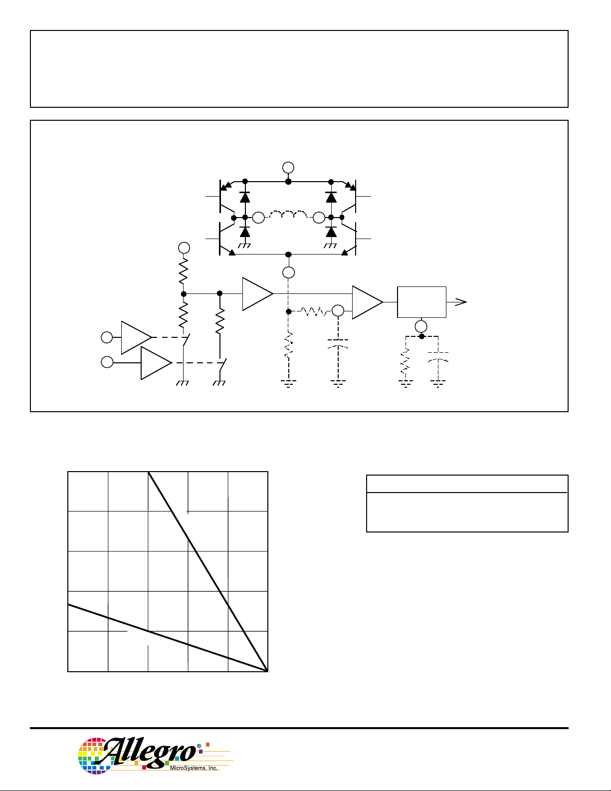
The UDN2917EB motor driver is designed to drive both windings
of a bipolar stepper motor or bidirectionally control two dc motors. Both
bridges are capable of sustaining 45 V and include internal pulse-width modula-
tion (PWM) control of the output current to 1.5 A.
For PWM current control, the maximum output current is determined by the
user’s selection of a reference voltage and sensing resistor. Two logic-level
inputs select output current limits of 0, 33%, 67%, or 100% of the maximum
level. A PHASE input to each bridge determines load current direction. Active-
low ENABLE inputs control the four drivers in each bridge.
The bridges include both ground clamp and flyback diodes for protection
against inductive transients. Internally generated delays prevent cross-over
currents when switching current direction. Special power-up sequencing is not
required. Thermal protection circuitry disables the outputs if the chip tempera-
ture exceeds safe operating limits.
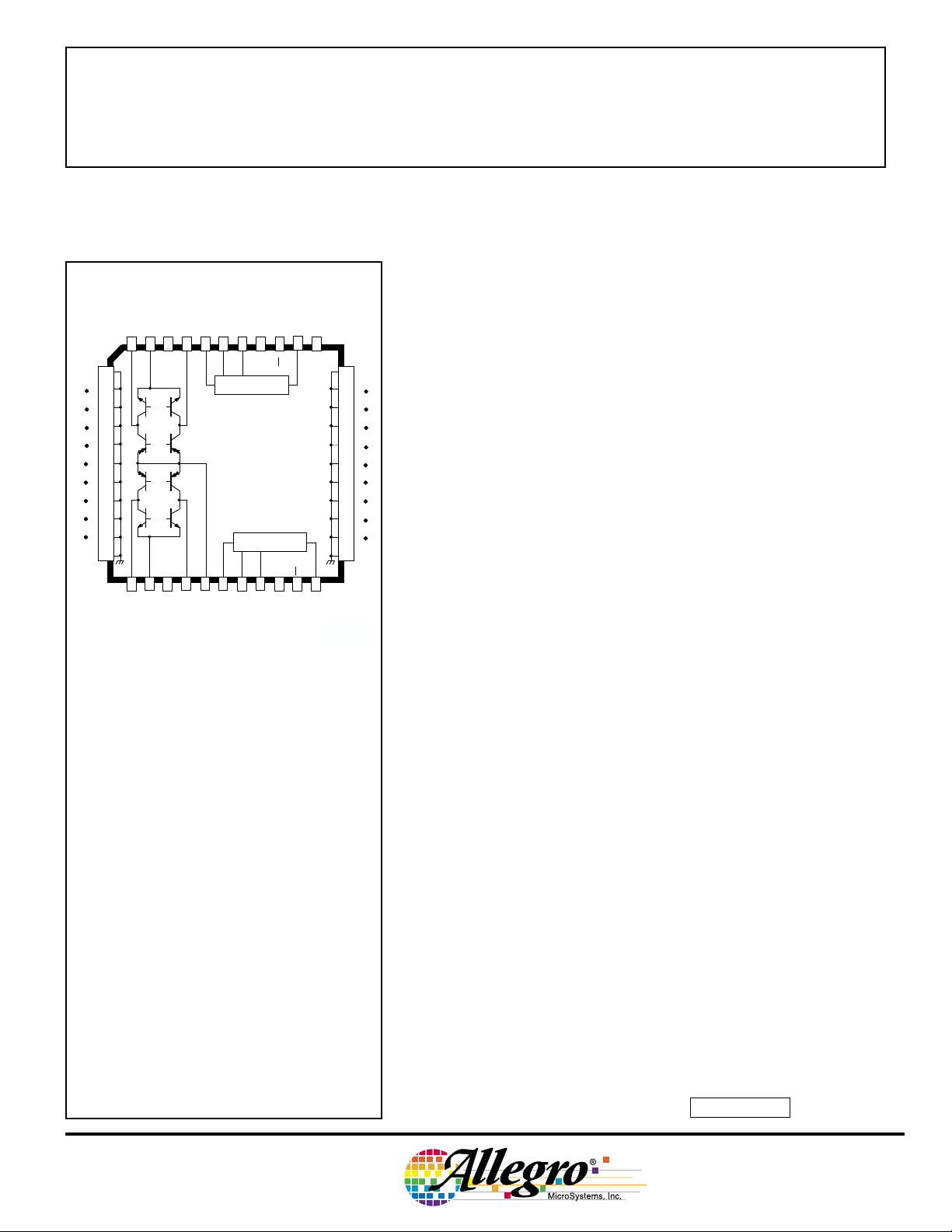
The UDN2917EB is supplied in a 44-lead power PLCC for surface-mount
applications. Its batwing construction provides for maximum package power
dissipation in the smallest possible construction. The UDN2917EB is available
for operation from -40°C to +85°C. To order, change the prefix from 'UDN' to
'UDQ'. This device is also available on special order for operation to +125°C.
Data Sheet
Motor Supply Voltage, VBB.................... 45 V
Output Current, I
(tw ≤ 20 µs) ..... ±1.75 A
OUT
(Continuous) ............................... ±1.5 A
Logic Supply Voltage, V
.................... 7.0 V
CC
Logic Input Voltage Range,
VIN................................ -0.3 V to +7.0 V
Output Emitter Voltage, V
................... 1.0 V
E
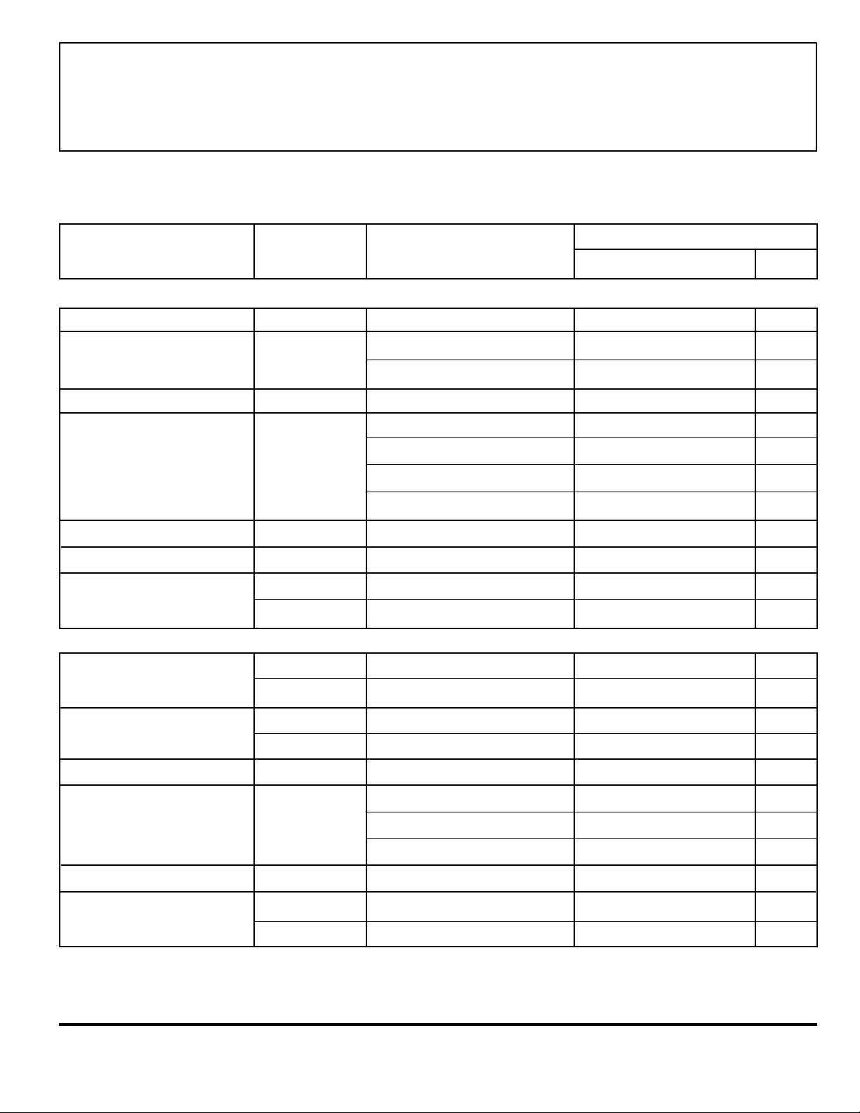
Package Power Dissipation,
PD......................................... See Graph
Operating Temperature Range,
T
.................................. -20°C to +85°C
A
Storage Temperature Range,
T
................................ -55°C to +150°C
S
Output current rating may be limited by duty cycle,
ambient temperature, and heat sinking. Under any
set of conditions, do not exceed the specified peak
current rating or a junction temperature of +150°C.
FEATURES
■ 1.5 A Continuous Output Current
■ 45 V Output Sustaining Voltage
■ Internal Clamp Diodes
■ Digital Control of Output Current
■ Internal Thermal Shutdown Circuitry
■ Similar to Dual PBL3770
Always order by complete part number: UDN2917EB .
2917
DUAL FULL-BRIDGE
PWM MOTOR DRIVER
PWM CURRENT-CONTROL CIRCUITRY
CHANNEL 1
PIN NUMBERS
SHOWN.
V
44
REF
20 kΩ
OUT
V
BB
22
OUT
B
36
A
5
E
12.5
10
7.5
÷10
40 kΩ
10 kΩ
2
I
0
1
I
1
R
S
R
C
SENSE
–
4
+
C
C
ONE
SHOT
41
RC
R
T
SOURCE
DISABLE
C
T
Dwg. EP-007-2A
TRUTH TABLE
R
=
θJT
Enable Phase Out
6
°C
/W
LHHL
LLLH
A
HXZZ
X = Don’t care
Z = High impedance
Out
B
5.0
2.5
0
ALLOWABLE PACKAGE POWER DISSIPATION IN WATTS
25
R = 30
θ
J
A
°C/W
50 75 100 125 150
TEMPERATURE IN °C
Dwg. GP-020B
115 Northeast Cutoff, Box 15036
Worcester, Massachusetts 01615-0036 (508) 853-5000
Copyright © 1991, 2000 Allegro MicroSystems, Inc.
2917
DUAL FULL-BRIDGE
PWM MOTOR DRIVER
ELECTRICAL CHARACTERISTICS at T
= +25°C, VBB = 45 V, VCC = 5.0 V, V
A
= 5.0 V (unless
REF
otherwise noted).
Limits
Characteristic Symbol Test Conditions Min. Typ. Max. Units
Output Drivers (OUT
Motor Supply Range V
Output Leakage Current I
Output Sustaining Voltage V
Output Saturation Voltage V
Clamp Diode Leakage Current I
Clamp Diode Forward Voltage V
Driver Supply Current I
Control Logic
or OUTB)
A
BB
CEX
CE(sus)
CE(SAT
R
F
BB(ON)
I
BB(OFF)
10 — 45 V
V
= V
OUT
BB
= 0 — <-1.0 -50 µA
V
OUT
I
= ±1.5 A, L = 3.5 mH 45 —— V
OUT
)
Sink Driver, I
Sink Driver, I
Source Driver, I
Source Driver, I
= +1.0 A* — 0.5 0.7 V
OUT
= +1.5 A* — 0.8 1.0 V
OUT
= -1.0 A* — 1.8 1.9 V
OUT
= -1.5 A* — 1.9 2.1 V
OUT
— <1.0 50 µA
VR = 45 V — <1.0 50 µA
IF = 1.5 A — 1.6 2.0 V
Both Bridges On, No Load — 9.0 12 mA
Both Bridges Off — 4.0 6.0 mA
Input Voltage V
Input Current I
Reference Voltage Range V
Current Limit Threshold V
(at trip point)
Thermal Shutdown Temp. T
Total Logic Supply Current I
IN(1)
V
IN(0)
IN(1)
I
IN(0)
REF
REF/VSENSE
J
CC(ON)
I
CC(OFF)
All Inputs 2.4 —— V
All Inputs ——0.8 V
V
= 2.4 V — <1.0 20 µA
IN
VIN = 0.8 V — -3.0 -200 µA
Operating 1.5 — 7.5 V
I0 = I1 = 0.8 V 9.5 10 10.5 —
= 2.4 V, I1= 0.8 V 13.5 15 16.5 —
I
0
= 0.8 V, I1 = 2.4 V 25.5 30 34.5 —
I
0
I0 = I1 = VEN = 0.8 V, No Load — 90 105 mA
I0 = I1 = 2.4 V, No Load — 10 12 mA
Negative current is defined as coming out of (sourcing) the specified device pin.
Typical Data is for design information only.
* Pulse test (<10 ms).
www.allegromicro.com
— 170 — °C
 Loading...