

Allegro UDN5713M Datasheet
5713
DUAL PERIPHERAL AND POWER DRIVER
5713
DUAL PERIPHERAL AND POWER DRIVER
— TRANSIENT PROTECTED OUTPUTS
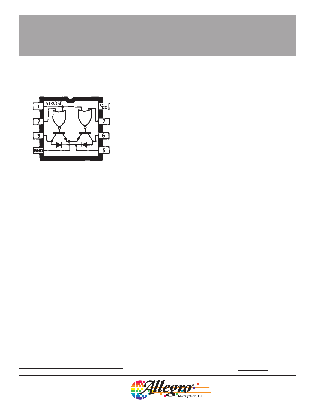
This “mini-DlP” dual peripheral and power driver is a bipolar
monolithic integrated circuit incorporating NOR logic gates, highcurrent switching transistors, and transient suppression diodes on the
same chip. The two output transistors are capable of simultaneously
sinking 300 mA continuously at ambient temperatures of up to +70°C.
In the OFF state, this driver will withstand at least 80 V.
The UDN5713M dual driver is ideally suited for interface between
low-level or high-level logic and high-current/high-voltage loads.
Typical applications include driving peripheral loads such as incandescent lamps, light-emitting diodes, memories, and heaters with a load
current of up to 600 mA.
Data Sheet
29307B
Dwg. No. A-9789
The integral transient suppression diodes allow the use of these
drivers with inductive loads such as relays, solenoids, or stepping
motors without the need for discrete diodes. Similar devices with four
drivers per package are the 5703 and 5706.
FEATURES
■ DTL/TTL/PMOS/CMOS Compatible Inputs
■ Low Input Current
ABSOLUTE MAXIMUM RATINGS
Supply Voltage, VCC. . . . . . . . . . . . . . 7.0 V
Input Voltage, VIN. . . . . . . . . . . . . . . . . 30 V
Output Off-State Voltage,
V
. . . . . . . . . . . . . . . . . . . . . . . . 80 V
OFF
Output On-State Sink Current,
I
. . . . . . . . . . . . . . . . . . . . . . 600 mA
ON
Suppression Diode Off-State Voltage,
V
. . . . . . . . . . . . . . . . . . . . . . . . 80 V
OFF
Suppression Diode On-State Current,
I
. . . . . . . . . . . . . . . . . . . . . . 600 mA
ON
Power Dissipation at T
DISCONTINUED PRODUCT
Package. . . . . . . . . . . . . . . . . . . 1.5 W*
Each Driver . . . . . . . . . . . . . . . . . 0.8 W
Operating Free-Air Temperature Range,
T
Storage Temperature Range,
T
*Derate at the rate of 12.5 mW/°C above
TA = 25°C.
— FOR REFERENCE ONLY
. . . . . . . . . . . . . . . . . -20°C to +85°C
A
. . . . . . . . . . . . . . . . -55°C to +150°C
S
= 25°C, P
A
D
■ 300 mA Continuous Output Current
■ Stand-off Voltage of 80 V
Always order by complete part number, e.g., UDN5713M .
5713
DUAL PERIPHERAL AND POWER DRIVER
RECOMMENDED OPERATING CONDITIONS
Min. Nom. Max. Units
Supply Voltage (V
) 4.75 5.0 5.25 V
CC
Operating Temperature Range 0 +25 +85 °C
Current into any output (ON state) — — 300 mA
ELECTRICAL CHARACTERISTICS over operating temperature range
(unless otherwise noted).
Test Conditions Limits
Driven Other
Characteristic Symbol Temp. V
“1” Input Voltage V
“0” Input Voltage V
IN(1)
IN(0)
— MIN — — — 2.0 — — V —
— MIN — — — — — 0.8 V —
CC
“0” Input Current at all
Inputs except Strobe I
“0” Input Current at Strobe I
IN(0)
IN(0)
— MAX 0.4 V 30 V — — -50 -100 µA 2
— MAX 0.4 V 30 V — — -100 -200 µA—
“1” Input Current at all
Inputs except Strobe I
“1” Input Current at Strobe I
Input Clamp Voltage V
IN(1)
IN(1)
IK
— MAX 30 V 0 V — — — 10 µA 2
— MAX 30 V 0 V — — — 20 µA—
— MIN -12 mA — — — — -1.5 V —
SWITCHING CHARACTERISTICS at VCC = 5.0 V, T
Input Input Output Min. Typ. Max. Units Notes
= 25°C
A
Limits
Characteristic Symbol Test Conditions Min. Typ. Max. Units Notes
Turn-on Delay Time t
Turn-off Delay Time t
NOTES: 1. Typical values are at VCC = 5.0 V, TA = 25°C.
2. Each input tested separately.
3. Voltage values shown in the test circuit waveforms are with respect to network ground terminal.
4. Capacitance values specified include probe and test fixture capacitance.
pd0
pd1
VS = 70 V, RL = 465 Ω (10 Watts), — 200 500 ns 3
C
= 15 pF
L
VS = 70 V, RL = 465 Ω (10 Watts), — 300 750 ns 3
C
= 15 pF
L
INPUT PULSE CHARACTERISTICS
V
= 0 V t
IN(0)
= 3.5 V t
V
IN(1)
115 Northeast Cutoff, Box 15036
Worcester, Massachusetts 01615-0036 (508) 853-5000
W
Copyright © 1976, 1997, Allegro MicroSystems, Inc.
= 7 ns tp = 1 µs
f
= 14 ns PRR = 500 kHz
r
 Loading...