

Allegro UDN3626M, UDN3625M Datasheet
CONTACT FACTORY
for availability
and latest information
ABSOLUTE MAXIMUM RATINGS
3625
AND
3626
POWERHALL® SENSOR/DRIVERS
FOR BRUSHLESS DC MOTORS
Requiring a minimum of external components, the UDN3625M
and UDN3626M are monolithic ICs that provide single-chip control
and direct drive solutions for many small, single-phase, unipolar
brushless dc motor applications. Integrated into the ICs are a highsensitivity Hall-effect sensor, control and commutating logic, a stable
voltage regulator, extensive self and system protective functions, and
two high-current saturated npn outputs. Both ICs include thermal
shutdown, output over-current limiting, and output transient protection/
flyback diodes. The UDN3625M is nominally for 12 V motor applications while the UDN3626M is better suited to 24 V motors.
Output over-current limiting (relating to startup surge or a locked
rotor condition) and short-circuit protection are provided by an internal
current-sense resistor. The maximum (default) output load current is
typically 1.3 A for the UDN3625M or 600 mA for the UDN3626M,
but may be decreased by user selection of an external low-wattage
resistor.
A separate low-level output provides tachometer capability for
motor speed control or sensing a locked rotor condition. With appropriate external logic, pulse-width modulated (PWM) speed control can
be accomplished at the output current adjust pin.
Data Sheet
27690A
Supply Voltage, VCC. . . . . . . . . . See Table
Output Current, I
PWM Current Control Voltage,
V
. . . . . . . . . . . . . See Applications
ADJ
Magnetic Flux Density, B . . . . . . Unlimited
Package Power Dissipation,
. . . . . . . . . . . . . . . . . . . . See Graph
P
D
Operating Temperature Range,
. . . . . . . . . . . . . . . . . -20°C to +85°C
T
A
Storage Temperature Range,
TS. . . . . . . . . . . . . . . . -65°C to +150°C
V
CC(MAX)
I
O(CONT)
I
O(PEAK)
Output current rating will be limited by
ambient temperature, supply voltage, and
duty cycle. Under any set of conditions, do
not exceed a junction temperature of
+150°C.
. . . . . . . . . . . . See Table
O
UDN3625M UDN3626M
14 V 26 V
1.0 A 0.45 A
1.6 A 0.75 A
These sensor/drivers are supplied in an 8-pin mini-DlP plastic
package with a copper leadframe for increased package power
handling capability.
FEATURES
■ 900 mA/12 V or 400 mA/24 V Operation
■ Speed-Control (PWM) Capability
■ Locked-Rotor Indication
■ Minimum External Components
■ Over-Current Protected
■ Thermal Protection
■ Enhanced Reliability
■ Reduced Cost
Always order by complete part number, e.g., UDN3625M .
See Maximum Ratings at left.
3625
POWERHALL
AND
3626
®
SENSOR/DRIVERS FOR
BRUSHLESS DC MOTORS
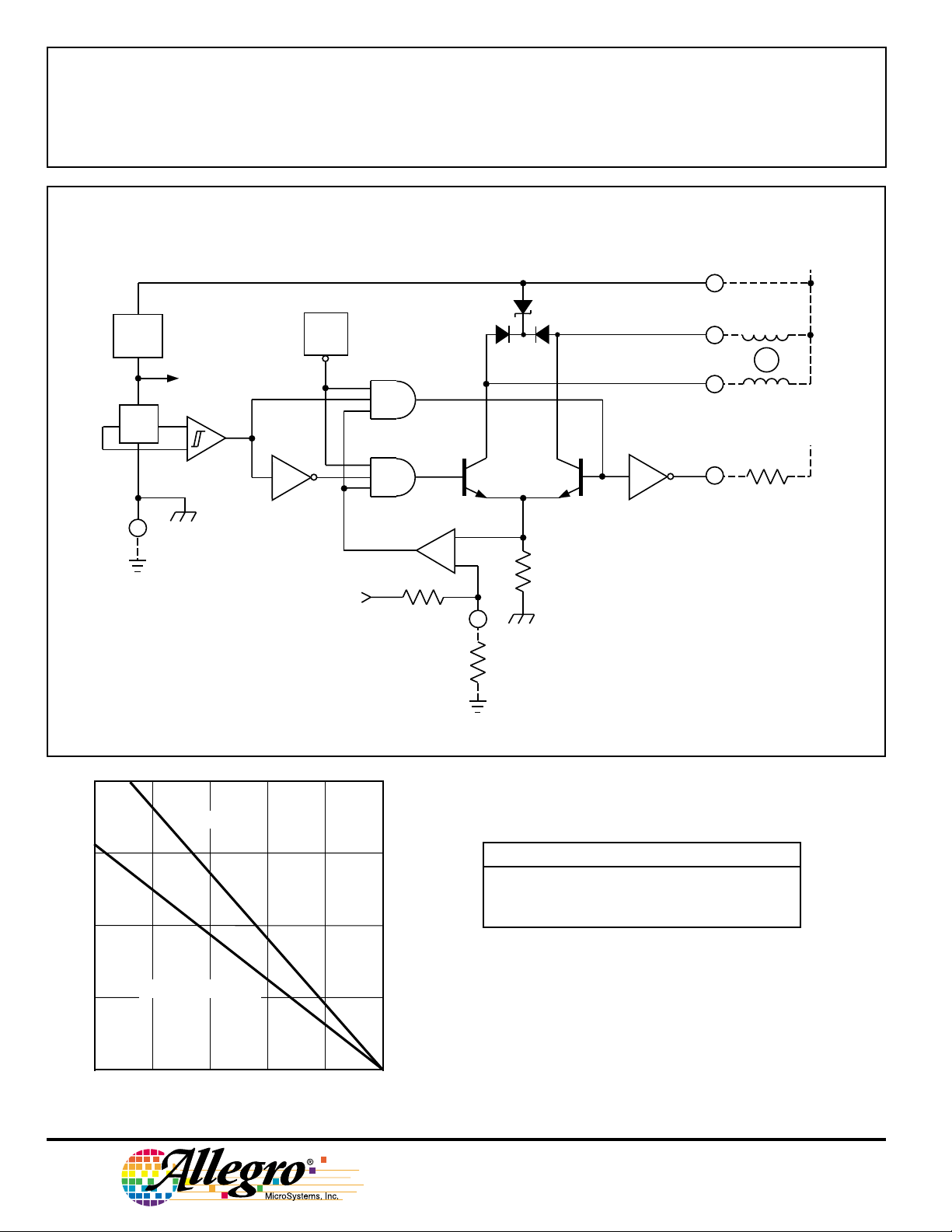
REG.
X
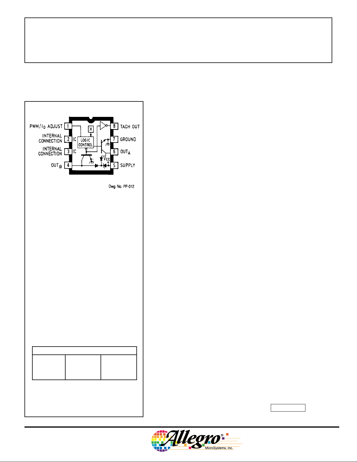
7
GROUND
TSD
FUNCTIONAL BLOCK DIAGRAM
SUPPLY
5
OUT
4
6
OUT
A
8
TACH
OUT
V
S
B
+V
2.0
R = 55°C/W
θJC
1.5
1.0
0.5
0
25
ALLOWABLE PACKAGE POWER DISSIPATION IN WATTS
FREE AIR, R = 80°C/W
50 75 100 125 150
θJA
TEMPERATURE IN °C
Dwg. GP-009-1B
PWM/I
ADJUST
1
O
R
ADJ
TRUTH TABLE
Mag. Field PWM/IOADJ OUTAOUT
> +B
OP
> -B
OP
Any <0.3 V High High
Open Low High
Open High Low
Dwg. FP-005-1
B
115 Northeast Cutoff, Box 15036
Worcester, Massachusetts 01615-0036 (508) 853-5000
Copyright © 1988, 1995, Allegro MicroSystems, Inc.
3625
AND
3626
POWERHALL
®
SENSOR/DRIVERS FOR
BRUSHLESS DC MOTORS
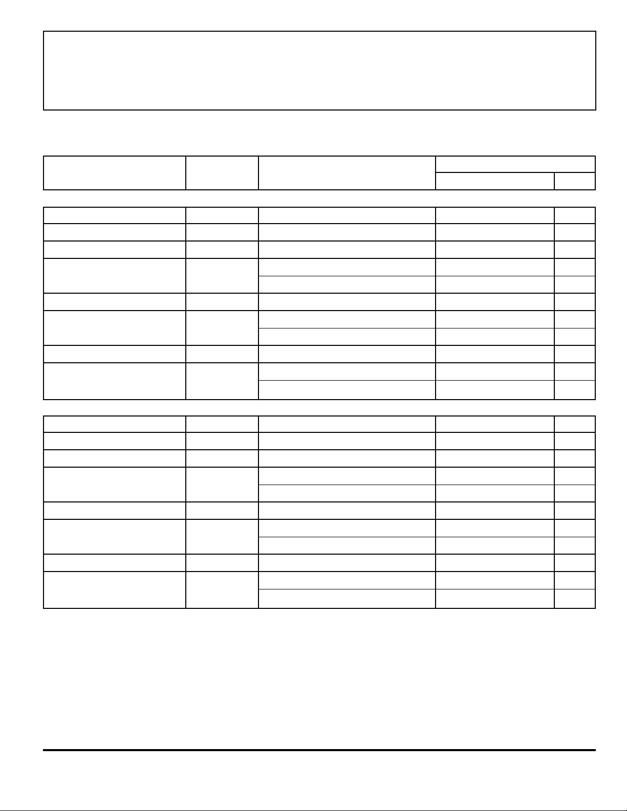
ELECTRICAL CHARACTERISTICS at T
= +25°C, R
A
= ∞, Over Operating Voltage Range
ADJ
(unless otherwise noted).
Limits
Characteristic Symbol Test Conditions Min. Typ. Max. Units
UDN3625M
Operating Voltage Range V
Output Leakage Current I
Output Breakdown Voltage V
Output Saturation Voltage V
S
O
(BR)CEX
O(SAT)
Output Current Limit IO MAX R
Output Clamp Voltage
V
CL
(Test Fig. 1)
Output Switching Time t
Supply Current
PLH
l
CC
(Test Fig. 2)
UDN3626M
VCC = VO = 24 V — — 100 µA
VCC = 24 V, lO = 10 mA* 34 — — V
IO = 450 mA, VS = 6.5 V — 0.25 0.4 V
IO = 900 mA, VS = 12 V — 0.5 0.8 V
= ∞, VO = 2 V 1.0 1.3 1.6 A
ADJ
ICL = 10 mA, VCC = 0 11 12 13 V
ICL = 450 mA=, VCC = 0 13 14 15 V
50% V
R
ADJ
R
ADJ
to VO = 3.0 V, lO = 450 mA — — 5.0 µs
ADJ
= ∞, VS = 14 V, One Output ON — 30 38 mA
= 0 Ω, VS = 14 V, Outputs OFF — 8.0 10 mA
6.5 12 14 V
Operating Voltage Range V
Output Leakage Current l
Output Breakdown Voltage V
Output Saturation Voltage V
S
O
(BR)CEX
O(SAT)
VCC = VO = 30 V — — 100 µA
VCC = 30 V, lO = 10 mA* 50 — — V
lO = 250 mA, VS = 6.5 V — 0.15 0.3 V
lO = 400 mA, VS = 24 V — 0.3 0.5 V
Output Current Limit lOMAX R
Output Clamp Voltage
V
CL
(Test Fig. 1)
Output Switching Time t
Supply Current l
PLH
CC
(Test Fig. 2)
= ∞, VO = 2 V 450 600 750 mA
ADJ
ICL = 10 mA, VCC = 0 17 18 20 V
ICL = 250 mA, VCC = 0 19 20 22 V
50% V
R
ADJ
R
ADJ
to VO = 3.0 V, lO = 250 mA — — 5.0 µs
ADJ
= ∞, VS = 26 V, One Output ON — — 24 mA
= 0 Ω, VS = 26 V, Outputs OFF — 8.0 10 mA
*lO is almost entirely Zener clamp current.
† Pulse test.
‡ Dependent on value of external series Zener diode (see Applications), 6.5 V without a Zener diode.
‡2426 V
Continued next page...
 Loading...