

Allegro UDN2962W Datasheet
GROUND
SENSE
SINK
SOURCE
THS
V
SOURCE
SINK
SENSE
THS
2962
DUAL SOLENOID/MOTOR DRIVER
—PULSE-WIDTH MODULATED CURRENT CONTROL
Using PWM to minimize power dissipation and maximize load
efficiency, the UDN2962W dual driver is recommended for impact
printer solenoids and stepper motors. It is comprised of two source/
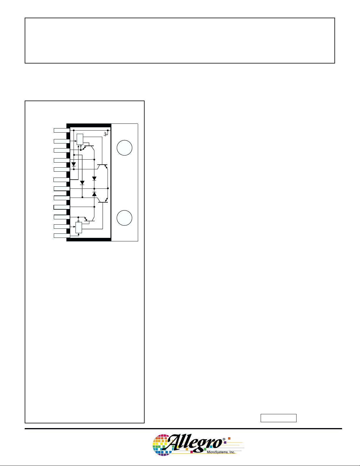
1
2
IN
A
A
43
A
5
A
6
A
7
CC
8
B
9
B
10
B
11
IN
B
12
B
LOGIC
LOGIC
Dwg. No. D-1001
sink driver pairs rated for continuous operation to ±3 A. It can be
connected to drive two independent loads or a single load in the fullbridge configuration. Both drivers include output clamp/flyback
diodes, input gain and level shifting, a voltage regulator for singlesupply operation, and pulse-width modulated output-current control
circuitry. Inputs are compatible with most TTL, DTL, LSTTL, and
low-voltage CMOS or PMOS logic.
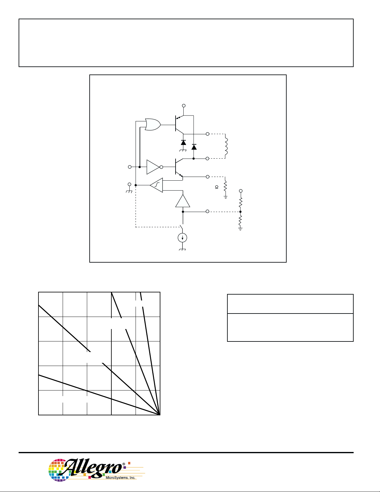
The peak output current and hysteresis for each source/sink pair is
set independently. Output current, threshold voltage, and hysteresis are
set by the user’s selection of external resistors. At the specified outputcurrent trip level, the source driver turns off. The internal clamp diode
then allows current to flow without additional input from the power
supply. When the lower current trip point is reached, the source driver
turns back on.
The UDN2962W is in a 12-pin single in-line power-tab package.
The tab is at ground potential and needs no insulation. For highcurrent or high-frequency applications, external heat sinking may be
required.
29319.12A†
Data Sheet
ABSOLUTE MAXIMUM RATINGS
at TJ ≤ +150°C
Supply Voltage, VCC. . . . . . . . . . . . . . 45 V
Peak Output Current, I
Input Voltage Range,
. . . . . . . . . . . . . . . - 0.3 V to +7.0 V
V
IN
Package Power Dissipation,
. . . . . . . . . . . . . . . . . . . See Graph
P
D
Operating Temperature Range,
. . . . . . . . . . . . . . . . -20°C to +85°C
T
A
Storage Temperature Range,
. . . . . . . . . . . . . . . -55°C to +150°C
T
S
NOTE: Output current rating may be limited by
duty cycle, ambient temperature, and heat
sinking. Under any set of conditions, do not
exceed the specified peak current and a junction
temperature of +150°C.
. . . . . . . . . ±4 A
OUT
FEATURES
■ 4 A Peak Output
■ 45 V Min. Sustaining Voltage
■ Internal Clamp Diodes
■ TTL/PMOS/CMOS Compatible Inputs
■ High-Speed Chopper
Always order by complete part number: UDN2962W .
2962
DUAL PWM
SOLENOID/MOTOR DRIVER
FUNCTIONAL BLOCK DIAGRAM
(ONE OF TWO DRIVERS)
IN
GND
+
_
-10
V
CC
SOURCE
SINK
SENSE
R
S
(TYP.0.1 )
THS
LOAD
V
REF
R
H
R
T
Dwg. No. D-1002
10
R = 2.0°C/W
θJT
8
3.0°C/W HEAT SINK
R = 5.0°C/W
θJA
V
IN
High NA Off Off
Low <V
Low >V
6
12°C/W HEAT SINK
R = 14°C/W
4
2
FREE AIR, R = 38°C/W
θJA
θJA
TRUTH TABLE
SOURCE SINK
V
SENSE
/10 On On
THS
/10 Off On
THS
DRIVER DRIVER
0
ALLOWABLE PACKAGE POWER DISSIPATION IN WATTS
25
50 75 100 125 150
TEMPERATURE IN °C
Dwg. GP-012B
115 Northeast Cutoff, Box 15036
W
Worcester, Massachusetts 01615-0036 (508) 853-5000
Copyright © 1986, 2000 Allegro MicroSystems, Inc.
2962
DUAL PWM
SOLENOID/MOTOR DRIVER
ELECTRICAL CHARACTERISTICS at TA = +25°C, TJ ≤ +150°C, VCC = 45 V, V
otherwise noted).
= 0 V (unless
SENSE
Limits
Characteristic Symbol Test Conditions Min. Typ. Max. Units
Supply Voltage Range V
CC
Operating 20 — 45 V
Output Drivers
Output Leakage Current I
Output Saturation Voltage V
Output Sustaining Voltage V
CE(SAT)
CE(sus)
Output Current Regulation ∆I
Clamp Diode Forward Voltage V
Output Rise Time t
Output Fall Time t
CEX
OUT
F
r
f
V
= 2.4 V, V
IN
V
= 2.4 V, V
IN
Source Drivers, I
Source Drivers, I
Sink Drivers, I
Sink Drivers, I
I
= ±3.0 A, L = 3.5 mH 45 — — V
OUT
V
= 0.6 V to 1.0 V, L = 3.5 mH — — ±25 %
THS
V
= 1.0 V to 2.0 V, L = 3.5 mH — — ±10 %
THS
V
= 2.0 V to 5.0 V, L = 3.5 mH — — ±5.0 %
THS
= 0 V — <-1.0 -100 µA
SOURCE
= 45 V — <1.0 100 µA
SINK
= 3.0 A — 2.1 2.3 V
LOAD
= 1.0 A — 1.7 2.0 V
LOAD
= 3.0 A — 1.7 2.0 V
LOAD
= 1.0 A — 1.1 1.3 V
LOAD
IF = 3.0 A — 1.7 2.0 V
I
= 3.0 A, 10% to 90%, Resistive Load — 0.5 1.0 µs
LOAD
I
= 3.0 A, 90% to 10%, Resistive Load — 0.5 1.0 µs
LOAD
Control Logic
Logic Input Voltage V
Logic Input Current I
V
THS/VSENSE
Ratio — At Trip Point, V
Supply Current l
(Total Device)
Propagation Delay Time t
(Resistive Load)
* Where V
SENSE
≥ V
THS
/9.5
IN(1)
V
IN(0)
IN(1)
I
IN(0)
I
THS(ON)
I
THS(HYS)
CC
pd
VIN = 2.4 V — 1.0 10 µA
VIN = 0.8 V — -20 -100 µA
V
≥ 500 mV, V
THS
V
SENSE
≥ V
THS
/9.5, V
THS
≤ V
SENSE
THS
/10.5 — -2.0 — µA
THS
= 0.6 V to 5.0 V 140 200 260 µA
= 2.0 V to 5.0 V 9.5 10 10.5 —
VIN = 2.4 V, Outputs Off — 8.0 12 mA
V
= 0.8 V, Outputs Open — 25 40 mA
IN
50% VIN to 50% V
50% V
100% V
to 50% V
IN
SENSE
to 50% V
, Turn Off — — 2.5 µs
OUT
, Turn On — — 3.0 µs
OUT
* — — 3.0 µs
OUT
NOTE: Negative current is defined as coming out of (sourcing) the specified device pin.
2.4 — — V
— — 0.8 V
www.allegromicro.com
 Loading...