

Allegro UCQ5833EP, UCQ5833A Datasheet
Designed to reduce logic supply current, chip size, and system
cost, the UCN5833A/EP integrated circuits offer high-speed operation
for thermal printers. These devices can also be used to drive multiplexed LED displays or incandescent lamps within their 125 mA peak
output current rating. The combination of bipolar and MOS technologies gives BiMOS II smart power ICs an interface flexibility beyond the
reach of standard buffers and power driver circuits.
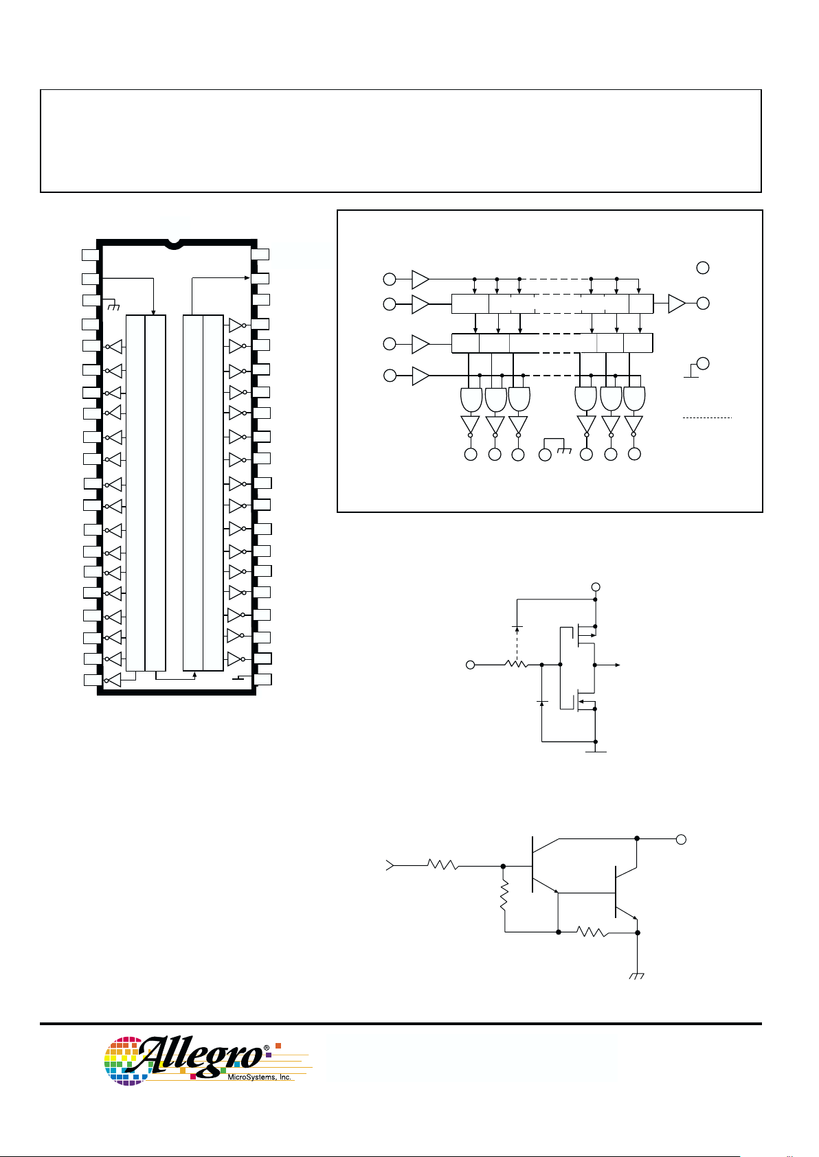
These 32-bit drivers have bipolar open-collector npn Darlington
outputs, a CMOS data latch for each of the drivers, a 32-bit CMOS
shift register, and CMOS control circuitry. The high-speed CMOS shift
registers and latches allow operation with most microprocessor-based
systems at data input rates above 3.3 MHz. Use of these drivers with
TTL may require input pull-up resistors to ensure an input logic high.
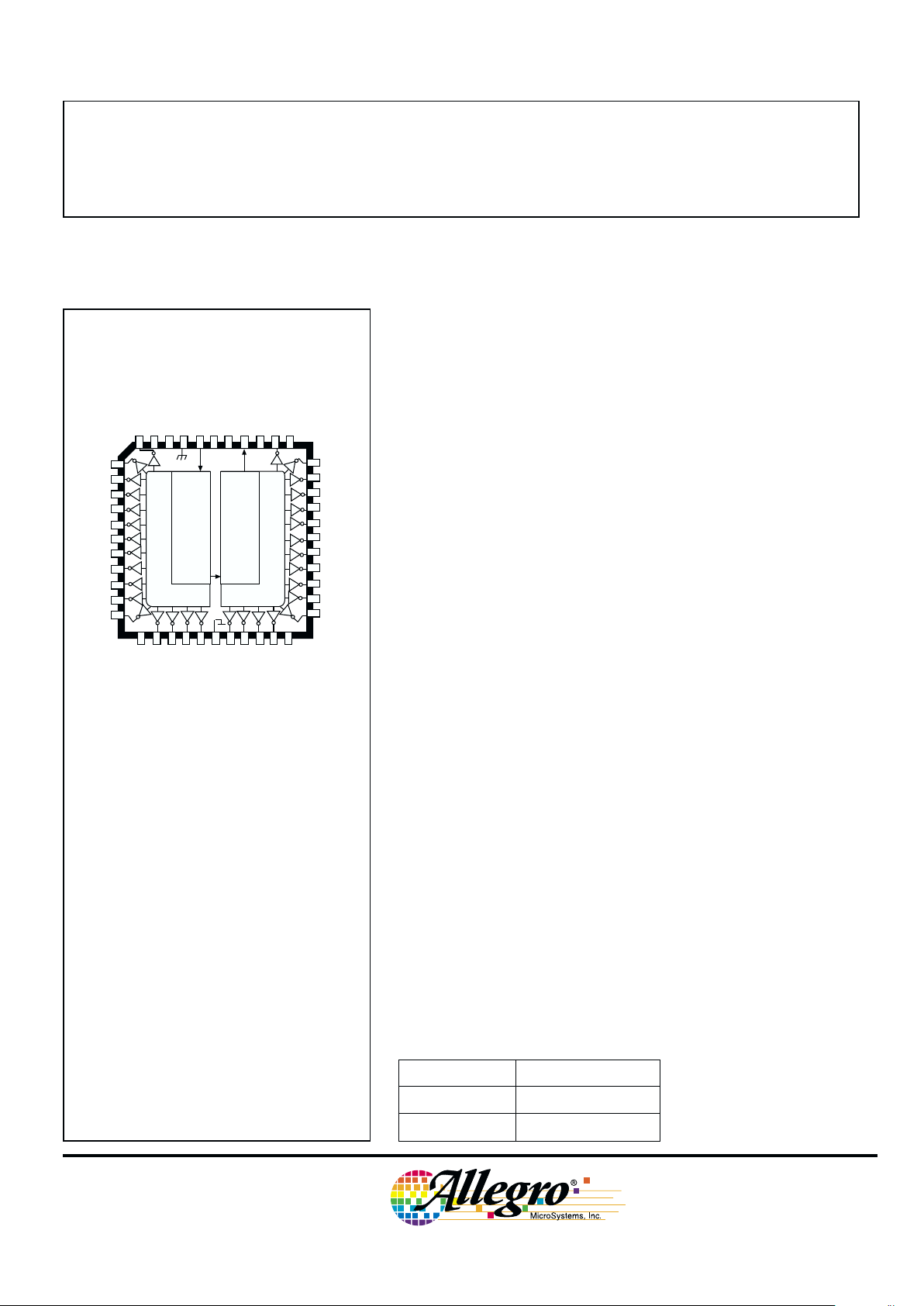
The UCN5833A is supplied in a 40-pin dual in-line plastic package
with 0.600" (15.24 mm) row spacing. At an ambient temperature of
+75°C, all outputs of the DlP-packaged device will sustain 50 mA
continuously. For high-density applications, the UCN5833EP is
available. This 44-lead plastic chip carrier (quad pack) is intended
for surface-mounting on solder lands with 0.050" (1.27 mm) centers.
CMOS serial data outputs permit cascading for applications requiring
additional drive lines.
FEATURES
■ To 3.3 MHz Data Input Rate
■ 30 V Minimum Output Breakdown
■ Darlington Current-Sink Outputs
■ Low-Power CMOS Logic and Latches
BiMOS II 32-BIT SERIAL-INPUT,
LATCHED DRIVER
UCN5833EP
ABSOLUTE MAXIMUM RATINGS
at +25°C Free-Air Temperature
Output Voltage, V
OUT
. . . . . . . . . . . 30 V
Logic Supply Voltage, V
DD
. . . . . . . 7.0 V
Input Voltage Range,
V
IN
. . . . . . . . . -0.3 V to V
DD
+ 0.3 V
Continuous Output Current,
l
OUT
(each output) . . . . . . . . . . 125 mA
Package Power Dissipation, P
D
(UCN5833A) . . . . . . . . . . . . . . . 3.5 W*
(UCN5833EP) . . . . . . . . . . . . . . 2.5 W*
Operating Temperature Range,
T
A
. . . . . . . . . . . . . . - 20°C to +85°C
Storage Temperature Range,
T
S
. . . . . . . . . . . . . -55°C to +150°C
* Derate linearly to 0 W at +150°C.
Caution: CMOS devices have input static protection
but are susceptible to damage when exposed to
extremely high static electrical charges.
Always order by complete part number:
Part Number Package
UCN5833A 40-Pin DIP
UCN5833EP 44-Lead PLCC
Dwg. No. A-13,049
1
4
5
6
18
1920212223
24
252627
28
40
41
42
43
44
2
3
7
8
9
10
11
12
13
14
15
16
17
OUT
2
OUT
3
OUT
4
OUT
5
OUT
6
OUT
7
OUT
8
OUT
9
OUT
OUT
10
OUT
11
12
OUTNCSTROBE1POWER GROUND
SERIAL DATA IN
LOGIC
SUPPLY
CLOCK
SERIAL DATA OUT
OUTPUT ENABLENCOUT
32
38
39
37
36
35
34
33
32
31
30
29
OUT
31
OUT
30
OUT
29
OUT
28
OUT
27
OUT
26
OUT
25
OUT
24
OUT
23
OUT
22
OUT
21
NC
OUT
13
OUT
14
OUT
15
OUT
16
LOGIC GROUND
OUT
17
OUT18OUT
19
OUT
20
NC
SUB
REGISTER
REGISTER
LATCHES
LATCHES
ST
CLK
OE
V
DD
Data Sheet
26185.16A*
5833
5833
BiMOS II 32-BIT
SERIAL-INPUT,
LATCHED DRIVER
115 Northeast Cutoff, Box 15036
Worcester, Massachusetts 01615-0036 (508) 853-5000
V
CLK
DD
SERIAL
DATA I N
POWER
GROUND
STROBE
OUT
OUT
OUT
OUT
OUT
OUT
1
2
3
4
5
6
OUT
7
OUT
8
OUT
9
OUT
10
OUT
11
OUT
12
OUT
13
OUT
14
OUT
18
OUT
19
OUT
20
OUT
21
OUT
22
OUT
23
OUT
24
OUT
25
OUT
26
OUT
27
OUT
28
OUT
29
OUT
30
OUT
31
OUT
32
OUTPUT
ENABLE
LOGIC
SUPPLY
SERIAL
DATA O U T
LOGIC
GROUND
SUB
LOGIC
SUPPLY
40
39
38
37
34
35
36
31
32
33
30
22
29
28
27
26
25
24
23
21
1
2
3
4
7
6
5
10
9
8
11
12
12
14
15
16
17
18
19
20
ST
OUT
15
OUT
16
OUT
17
LATCHES
REGISTER
REGISTER
LATCHES
OE
Dwg. No. A-13,057
TYPICAL INPUT CIRCUIT
FUNCTIONAL BLOCK DIAGRAM
Dwg. No. A-13,048
Dwg. No. A-13,051
Dwg. No. A-13,050
TYPICAL OUTPUT DRIVER
UCN5833A
32-BIT SHIFT REGISTER
LATCHES
CLOCK
SERIAL
DATA I N
STROBE
OUTPUT
ENABLE
LOGIC
GROUND
V
DD
SERIAL DATA
OUT
SUB
MOS
BIPOLAR
OUT
OUT
OUT
OUT
OUT OUT
1
2
3
30
31
32
POWER
GROUND
IN
SUB
V
DD
OUT
115 Northeast Cutoff, Box 15036
Worcester, Massachusetts 01615-0036 (508) 853-5000
Copyright © 1986, 1995, Allegro MicroSystems, Inc.
CLOCK
5833
BiMOS II 32-BIT
SERIAL-INPUT,
LATCHED DRIVER
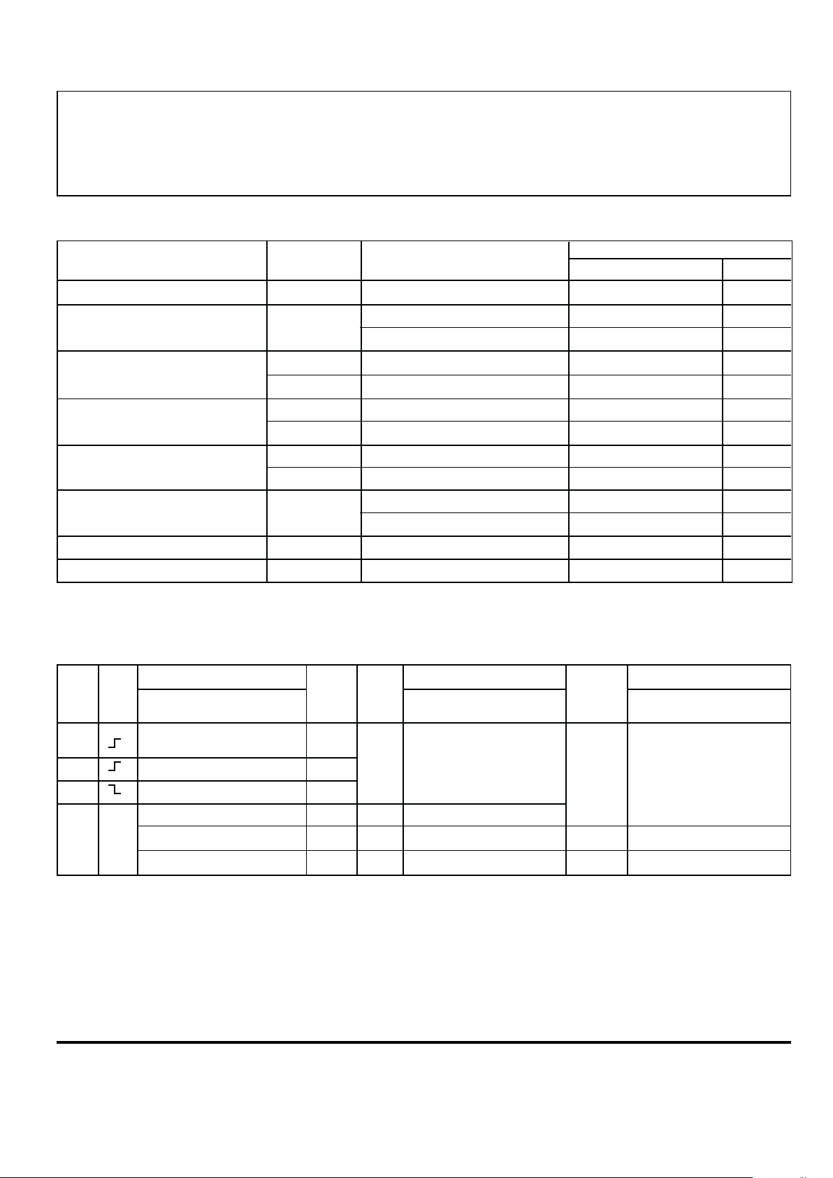
TRUTH TABLE
Serial Shift Register Contents Serial Latch Contents Output Output Contents
Data Clock Data Strobe Enable
Input Input I
1I2I3
... I
N-1IN
Output Input I1I2I3... I
N-1IN
Input I1I2I3... I
N-1
I
N
HHR
1R2
... R
N-2RN-1
R
N-1
LLR
1R2
... R
N-2RN-1
R
N-1
XR
1R2R3
... R
N-1RN
R
N
XXX...X X X L R1R2R3... R
N-1 RN
P1P2P3... P
N-1PN
P
N
HP1P2P3... P
N-1 PN
HP1P2P3... P
N-1
P
N
X X X ... X X L H H H ... H H
L = Low Logic Level H = High Logic Level X = Irrelevant P = Present State R = Previous State
ELECTRICAL CHARACTERISTICS at TA = +25°C, VDD = 5 V (unless otherwise noted).
Limits
Characteristic Symbol Test Conditions Min. Max. Units
Output Leakage Current I
CEX
V
OUT
= 30 V, TA = 70°C—10µA
Collector-Emitter V
CE(SAT)
l
OUT
= 50 mA — 1.2 V
l
OUT
= 100 mA — 1.7 V
Input Voltage V
IN(1)
3.5 5.3 V
V
IN(0)
-0.3 +0.8 V
Input Current l
IN(1)
VIN = 5.0 V — 1.0 µA
l
IN(0)
VIN = 0 V — -1.0 µA
Serial Output Voltage V
OUT(1)
I
OUT
= -200 µA 4.5 — V
V
OUT(0)
I
OUT
= 200 µA — 0.3 V
Supply Current l
DD
One output ON, l
OUT
= 100 mA — 1.0 mA
All outputs OFF — 50 µA
Output Rise Time t
r
l
OUT
= 100 mA, 10% to 90% — 500 ns
Output Fall Time t
f
l
OUT
= 100 mA, 90% to 10% — 500 ns
NOTE: Positive (negative) current is defined as going into (coming out of) the specified device pin.
Saturation Voltage
 Loading...