

Allegro UCN5810LWF, UCN5810EPF, UCN5810AF, UCQ5810LWF, UCQ5810EPF Datasheet
...
BiMOS II 10-BIT SERIAL-INPUT, LATCHED
SOURCE DRIVERS WITH ACTIVE-DMOS PULL-DOWNS
Always order by complete part number, e.g., UCN5810AF .
The UCN5810AF, UCN5810EPF, and UCN5810LWF combine a 10-bit
CMOS shift register and accompanying data latches, control circuitry, bipolar
sourcing outputs with DMOS active pull-downs. Designed primarily to drive
vacuum-fluorescent displays, the 60 V and -40 mA output ratings also allow
these devices to be used in many other peripheral power driver applications.
The UCN5810AF/EPF/LWF feature reduced supply requirements (active
DMOS pull-downs) and lower saturation voltages when compared with the
original UCN5810A.
The CMOS shift register and latches allow direct interfacing with
microprocessor-based systems. With a 5 V supply, they will operate to at
least 3.3 MHz. At 12 V, higher speeds are possible. Use with TTL may
require appropriate pull-up resistors to ensure an input logic high.
A CMOS serial data output enables cascade connections in applications
requiring additional drive lines. Similar devices are available as the
UCN5811A (12 bits), UCN5812AF/EPF (20 bits), and UCN5818AF/EPF (32
bits).
The UCN5810AF/EPF/LWF output source drivers are NPN Darlingtons
capable of sourcing up to 40 mA. The DMOS active pull-downs are capable
of sinking up to 15 mA. For inter-digit blanking, all of the output drivers can
be disabled and the DMOS sink drivers turned on by the BLANKING input
high.
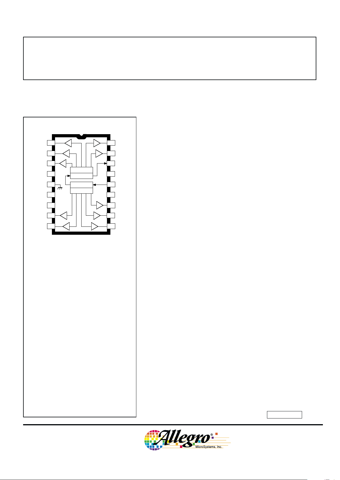
The UCN5810AF is furnished in an 18-pin dual in-line plastic package.
The UCN5810EPF is furnished in a 20-lead plastic chip carrier. The
UCN5810LWF is furnished in a wide-body, small-outline plastic package
(SOIC) with gull-wing leads. Copper lead frames, reduced supply current
requirements, and lower output saturation voltages allow all devices to source
25 mA from all outputs continuously, over the entire operating temperature
range. All devices are also available for operation between -40°C and +85°C.
To order, change the prefix from ‘UCN’ to ‘UCQ’.
FEATURES
■ High-Speed Source Drivers
■ 60 V Minimum
Output Breakdown
■ Improved Replacements
for TL4810B
UCN5810AF
Data Sheet
26182.24C
2
3
4
5
6
7
8
910
11
12
13
14
15
16
17
18
SERIAL
DATA OUT
LOAD
SUPPLY
SERIAL
DATA IN
BLANKING
LOGIC
SUPPLY
STROBE
GROUND
CLOCK
CLK
V
ST
BLNK
DD
BB
V
OUT
9
OUT
10
OUT
1
OUT
2
OUT
3
Dwg. PP-029
OUT
8
OUT
7
OUT
6
OUT
5
OUT
4
1
LATCHES
REGISTER
REGISTER
LATCHES
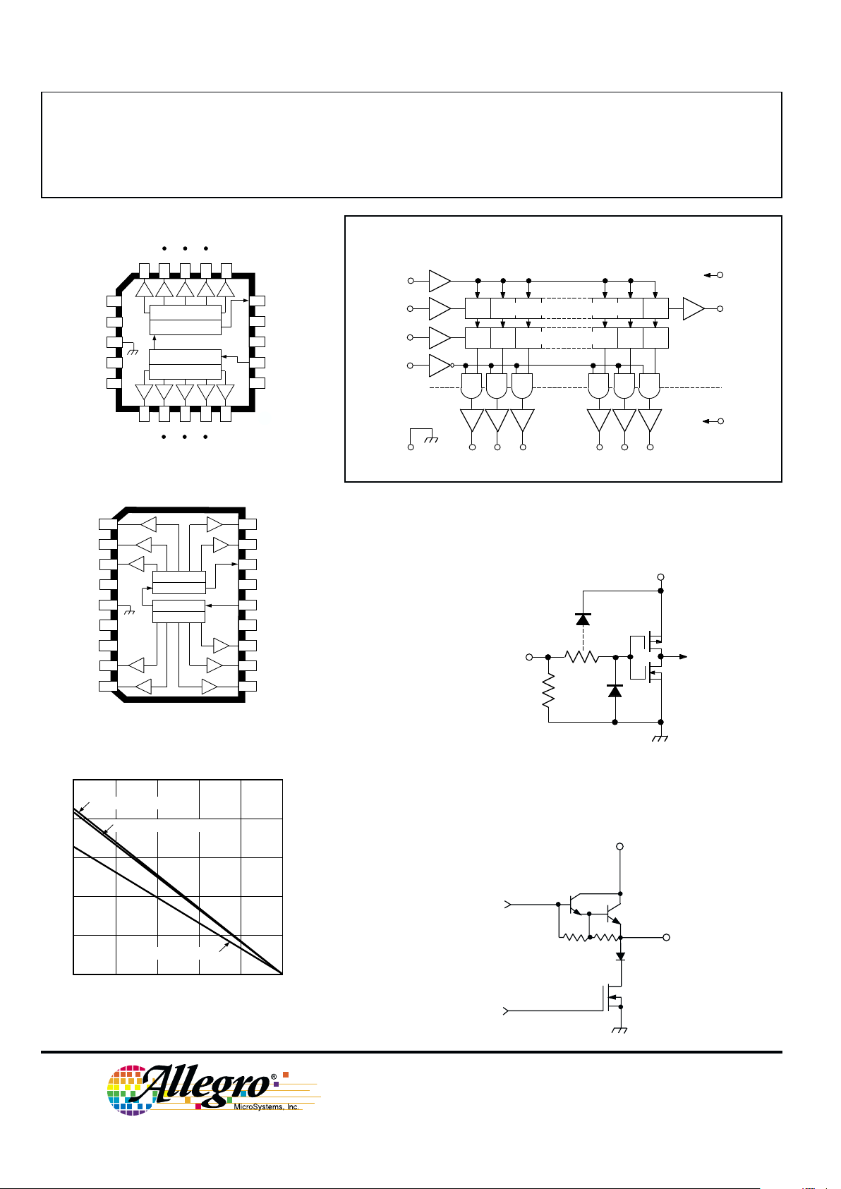
ABSOLUTE MAXIMUM RATINGS
at TA = 25°C
Logic Supply Voltage, VDD..................... 15 V
Driver Supply Voltage, V
BB
.................... 60 V
Continuous Output Current Range,
I
OUT
.......................... -40 mA to +15 mA
Input Voltage Range,
V
IN
........................ -0.3 V to VDD + 0.3 V
Package Power Dissipation, P
D
(UCN5810AF) ........................... 2.27 W*
(UCN5810EPF) ........................ 1.78 W*
(UCN5810LWF) ........................ 1.56 W*
Operating Temperature Range,
T
A
.................................. -20°C to +85°C
Storage Temperature Range,
T
S
................................ -55°C to +150°C
*Derate linearly to 0 W at +150°C.
Caution: CMOS devices have input static
protection but are susceptible to damage when
exposed to extremely high static electrical
charges.
Note that the UCN5810AF (dual in-line package)
and UCN5810LWF (small-outline IC package) are
electrically identical and share a common pin
number assignment.
■ Low Output Saturation Voltages
■ Low-Power CMOS Logic
and Latches
■ To 3.3 MHz Data Input Rate
■ Active DMOS Pull-Downs
5810 -F
5810-F
10-BIT SERIAL-INPUT,
LATCHED SOURCE DRIVERS
WITH ACTIVE-DMOS PULL-DOWNS
115 Northeast Cutoff, Box 15036
Worcester, Massachusetts 01615-0036 (508) 853-5000
FUNCTIONAL BLOCK DIAGRAM
UCN5810EPF
TYPICAL INPUT CIRCUIT
TYPICAL OUTPUT DRIVER
Dwg. No. A-14,219
50 75 100 125 150
2.5
0.5
0
ALLOWABLE PACKAGE POWER DISSIPATION IN WATTS
AMBIENT TEMPERATURE IN °C
2.0
1.5
1.0
25
SUFFIX 'A', R = 60°C/W
θJA
SUFFIX 'EP', R = 59°C/W
θJA
Dwg. GP-024B
SUFFIX 'LW', R = 80°C/W
θJA
Dwg. GP-024A
11
12
13
14
15
17
10
16
18
SERIAL
DATA OUT
LOAD
SUPPLY
SERIAL
DATA IN
BLANKING
OUT
9
OUT
10
OUT
1
OUT
2
OUT
3
Dwg. PP-029-1
1
2
3
8
9
4
5
6
7
LOGIC
SUPPLY
STROBE
GROUND
CLOCK
CLK
V
ST
BLNK
DD
BB
V
OUT
8
OUT
7
OUT
6
OUT
5
OUT
4
LATCHES
REGISTER
REGISTER
LATCHES
UCN5810LWF
14
15
16
17
18
1
2
3
4
5
6
7
8
9
10
11
12
13
19
20
STROBE
V
DD
Dwg. PP-059
OUT
1
OUT
10
OUT
5
OUT
6
LATCHES
REGISTER
REGISTER
LATCHES
V
BB
CLOCK
NC
GROUND
LOGIC
SUPPLY
SERIAL
DATA OUT
LOAD
SUPPLY
NC
SERIAL
DATA IN
BLANKING
ST
CLK
BLNK
Dwg. PP-029-1
V
OUT
BB
N
MOS
BIPOLAR
OUT1OUT
2
GROUND
Dwg. FP-013-1
OUT
3
OUT
N
CLOCK
SERIAL
DATA IN
STROBE
BLANKING
SERIAL
DATA OUT
SERIAL-PARALLEL SHIFT REGISTER
LATCHES
V
DD
V
BB
LOGIC
SUPPLY
LOAD
SUPPLY
Dwg. EP-010-4A
IN
V
DD
Copyright © 1988, 2000 Allegro MicroSystems, Inc.
5810-F
10-BIT SERIAL-INPUT,
LATCHED SOURCE DRIVERS
WITH ACTIVE-DMOS PULL-DOWNS
www.allegromicro.com
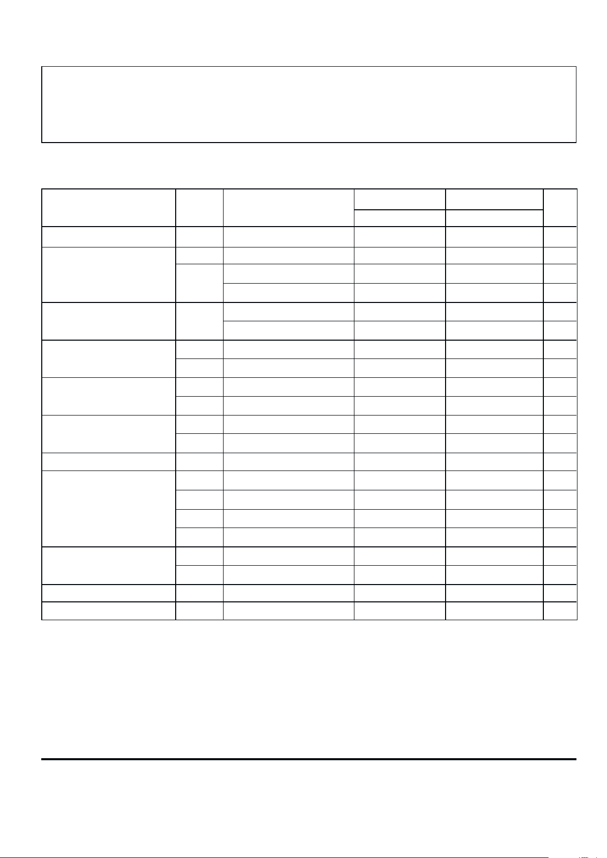
Limits @ VDD = 5 V Limits @ VDD = 12 V
Characteristic Symbol Test Conditions Mln. Typ. Max. Min. Typ. Max. Units
Output Leakage Current I
CEX
V
OUT
= 0 V, TA = +70°C — -5.0 -15 — -5.0 -15 µA
Output Voltage V
OUT(1)IOUT
= -25 mA 58 58.5 — 58 58.5 — V
V
OUT(0)IOUT
= 1 mA — 1.0 1.5 — — — V
I
OUT
= 2 mA — — — — 1.0 1.5 V
Output Pull-Down Current I
OUT(0)
V
OUT
= 5 V to V
BB
2.0 3.5 — — — — mA
V
OUT
= 20 V to V
BB
——— 8.013— mA
Input Voltage V
IN(1)
3.5 — 5.3 10.5 — 12.3 V
V
IN(0)
-0.3 — +0.8 -0.3 — +0.8 V
Input Current I
IN(1)
VIN = V
DD
— — 100 — — 240 µA
I
IN(0)
VIN = 0.8 V — -0.05 -0.5 — -0.1 -1.0 µA
Serial Data Output Voltage V
OUT(1)IOUT
= -200 µA 4.5 4.7 — 11.7 11.8 — V
V
OUT(0)IOUT
= 200 µA — 200 250 — 100 200 mV
Maximum Clock Frequency f
clk
3.3* — — — — — MHz
Supply Current I
DD(1)
All Outputs High — 100 300 — 200 500 µA
I
DD(0)
All Outputs Low — 100 300 — 200 500 µA
I
BB(1)
Outputs High, No Load — 0.7 2.0 — 0.7 2.0 mA
I
BB(0)
Outputs Low — 10 100 — 10 100 µA
Blanking to Output Delay t
PHL
CL = 30 pF, 50% to 50% — 2000 — — 1000 — ns
t
PLH
CL = 30 pF, 50% to 50% — 1000 — — 850 — ns
Output Fall Time t
f
CL = 30 pF, 90% to 10% — 1450 — — 650 — ns
Output Rise Time t
r
CL = 30 pF, 10% to 90% — 650 — — 700 — ns
Negative current is defined as coming out of (sourcing) the specified device pin.
* Operation at a clock frequency greater than the specified minimum value is possible but not warranteed.
ELECTRICAL CHARACTERISTICS at TA = +25°C, VBB = 60 V unless otherwise noted.
 Loading...