

5800
AND
5801
BiMOS II
LA TCHED DRIVERS
UCN5800L
141
UCN5800A
1
CLEAR
STROBE
GROUND
Note the UCN5800A (DIP) and the UCN5800L
(SOIC) are electrically identical and share a
common terminal number assignment.
2
3
IN
1
IN
4
2
5
IN
3
6
IN
4
78
LATCHES
V
ABSOLUTE MAXIMUM RATINGS
at +25°C Free-Air Temperature
Output Voltage, VCE. . . . . . . . . . . . . . 50 V
Supply Voltage, V
Input Voltage Range,
V
. . . . . . . . . . . -0.3 V to VDD + 0.3 V
IN
Continuous Collector Current,
l
. . . . . . . . . . . . . . . . . . . . . . 500 mA
C
Package Power Dissipation,
P
. . . . . . . . . . . . . . . . . . . . See Graph
D
Operating Temperature Range,
T
. . . . . . . . . . . . . . . . -20°C to +85°C
A
Storage Temperature Range,
T
. . . . . . . . . . . . . . . -55°C to +150°C
S
Caution: CMOS devices have input static
protection but are susceptible to damage when
exposed to extremely high static electrical
charges.
. . . . . . . . . . . . . . 15 V
DD
OUTPUT
14
ENABLE
13
SUPPLY
DD
12
OUT
11
OUT
10
OUT
9
OUT
COMMON
Dwg. PP-014A
Data Sheet
5800
AND
26180.10B
5801
BiMOS II LATCHED DRIVERS
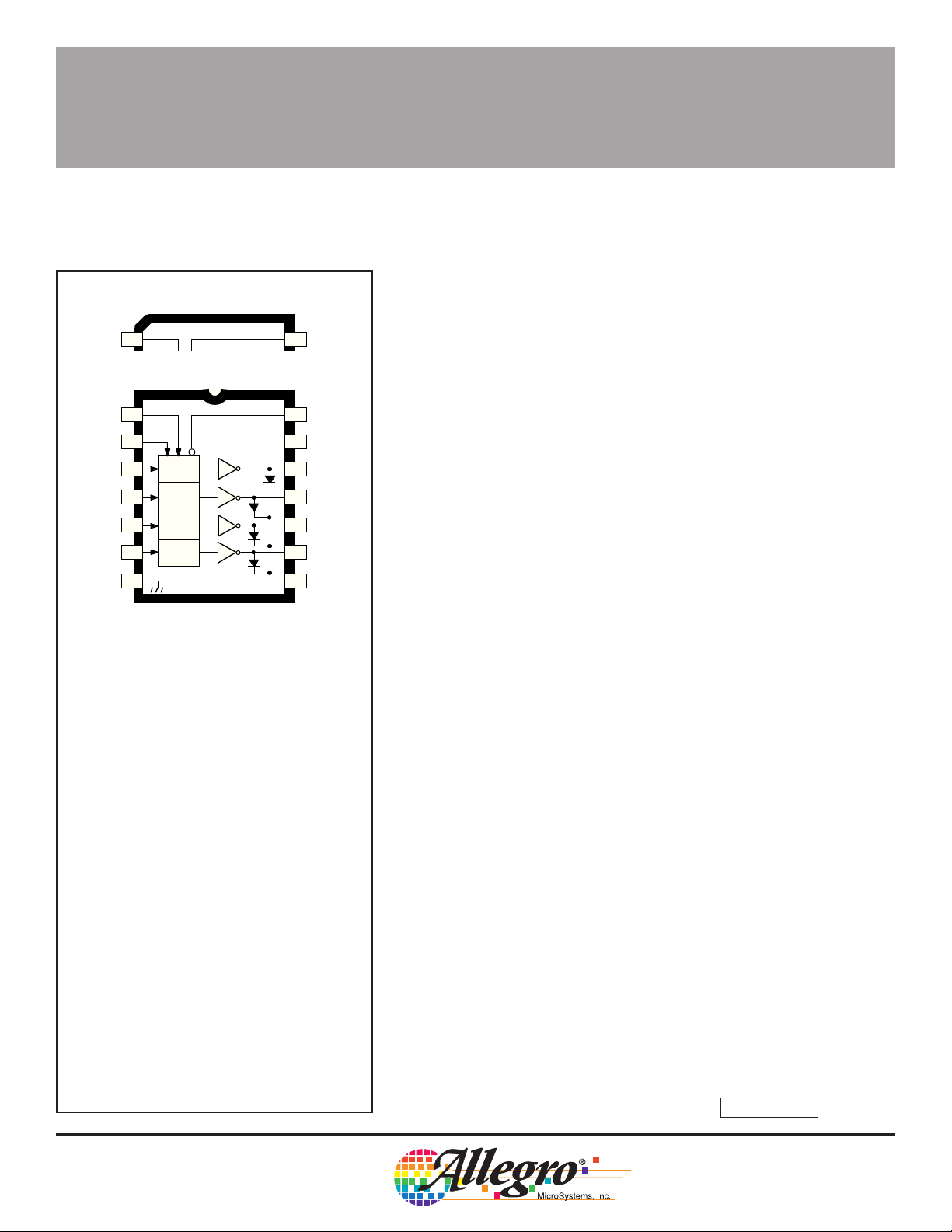
The UCN5800A/L and UCN5801A/EP/LW latched-input BiMOS
ICs merge high-current, high-voltage outputs with CMOS logic. The
CMOS input section consists of 4 or 8 data (‘D’ type) latches with
associated common CLEAR, STROBE, and OUTPUT ENABLE
circuitry. The power outputs are bipolar npn Darlingtons. This merged
technology provides versatile, flexible interface. These BiMOS power
interface ICs greatly benefit the simplification of computer or microprocessor I/O. The UCN5800A and UCN5800L each contain four latched
drivers; the UCN5801A, UCN5801EP, and UCN5801LW contain eight
latched drivers.
1
2
3
4
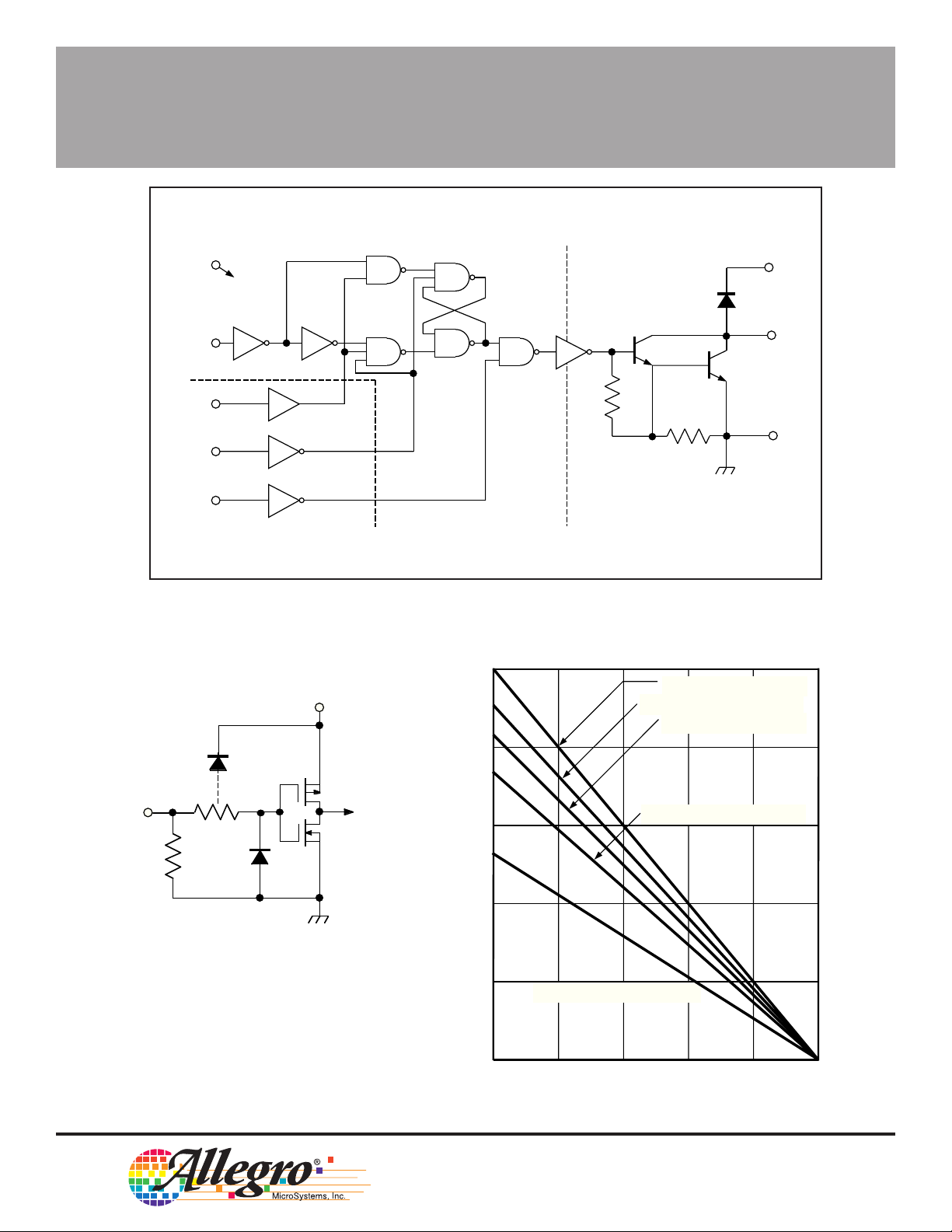
The UCN5800A/L and UCN5801A/EP/LW supersede the original
BiMOS latched-input driver ICs (UCN4400A and UCN4801A). These
second-generation devices are capable of much higher data input
rates and will typically operate at better than 5 MHz with a 5 V logic
supply. Circuit operation at 12 V affords substantial improvement over
the 5 MHz figure.
The CMOS inputs are compatible with standard CMOS and NMOS
circuits. TTL circuits may mandate the addition of input pull-up resistors. The bipolar Darlington outputs are suitable for directly driving
many peripheral/power loads: relays, lamps, solenoids, small dc
motors, etc.
All devices have open-collector outputs and integral diodes for
inductive load transient suppression. The output transistors are
capable of sinking 500 mA and will withstand at least 50 V in the OFF
state. Because of limitations on package power dissipation, the simultaneous operation of all drivers at maximum rated current can only be
accomplished by a reduction in duty cycle. Outputs may be paralleled
for higher load current capability.
The UCN5800A is furnished in a standard 14-pin DIP; the
UCN5800L and UCN5801LW in surface-mountable SOICs; the
UCN5801A in a 22-pin DIP with 0.400" (10.16 mm) row centers; the
UCN5801EP in a 28-lead PLCC.
FEATURES
■ To 4.4 MHz Data Input Rate
■ High-Voltage,
High-Current Outputs
■ Output Transient Protection
■ Internal Pull-Down Resistors
■ Low-Power CMOS Latches
■ Automotive Capable
■ CMOS, NMOS,
TTL Compatible Inputs
Always order by complete part number, e.g., UCN5801EP .
5800
AND
5801
BiMOS II
LA TCHED DRIVERS
SUPPLY
FUNCTIONAL BLOCK DIAGRAM
V
DD
IN
N
STROBE
CLEAR
OUTPUT ENABLE
COMMON MOS CONTROL
TYPICAL INPUT CIRCUIT
V
DD
TYPICAL MOS LATCH TYPICAL BIPOLAR DRIVE
2.5
22-PIN DIP, R = 50°C/W
28-LEAD PLCC, R = 55°C/W
14-PIN DIP, R = 60°C/W
2.0
COMMON
OUT
GROUND
Dwg. FP-016-1
θJA
θJA
θJA
N
IN
Dwg. EP-010-4A
115 Northeast Cutoff, Box 15036
Worcester, Massachusetts 01615-0036 (508) 853-5000
Copyright © 1985, 1997, Allegro MicroSystems, Inc.
1.5
1.0
0.5
ALLOWABLE PACKAGE POWER DISSIPATION IN WATTS
0
25
14-LEAD SOIC, R = 95°C/W
50 75 100 125 150
AMBIENT TEMPERATURE IN °C
24-LEAD SOIC, R = 68°C/W
θJA
θJA
Dwg. GP-023-1

5800
AND
5801
BiMOS II
LA TCHED DRIVERS
ELECTRICAL CHARACTERISTICS at T
= +25°C, V
A
= 5 V (unless otherwise noted).
DD
Limits
Characteristic Symbol Test Conditions Min. Typ. Max. Units
Output Leakage Current I
Collector-Emitter V
CEX
CE(SAT)
Saturation Voltage
Input Voltage V
Input Resistance r
Supply Current I
IN(0)
V
IN(1)
IN
DD(ON)
(Each
Stage)
I
DD(OFF)
(Total)
Clamp Diode I
Leakage Current
Clamp Diode Forward Voltage V
NOTE: Operation of these devices with standard TTL or DTL may require the use of appropriate pull-up resistors to ensure a minimum logic “1”.
R
F
VCE = 50 V, TA = +25°C——50µA
= 50 V, TA = +70°C — — 100 µA
V
CE
IC = 100 mA — 0.9 1.1 V
= 200 mA — 1.1 1.3 V
I
C
= 350 mA, VDD = 7.0 V — 1.3 1.6 V
I
C
— — 1.0 V
VDD = 12 V 10.5 — — V
= 10 V 8.5 — — V
V
DD
= 5.0 V (See Note) 3.5 — — V
V
DD
VDD = 12 V 50 200 — kΩ
= 10 V 50 300 — kΩ
V
DD
= 5.0 V 50 600 — kΩ
V
DD
VDD = 12 V, Outputs Open — 1.0 2.0 mA
= 10 V, Outputs Open — 0.9 1.7 mA
V
DD
= 5.0 V, Outputs Open — 0.7 1.0 mA
V
DD
VDD = 12 V, Outputs Open, Inputs = 0 V — — 200 µA
= 5.0 V, Outputs Open, Inputs = 0 V — 50 100 µA
V
DD
VR = 50 V, TA = +25°C——50µA
= 50 V, TA = +70°C — — 100 µA
V
R
IF = 350 mA — 1.7 2.0 V
UCN5801EP
(additional pinout diagrams
are on next page)
CLEAR
STROBE
2
4
3
ST
NC
5
IN
1
IN
6
2
IN
7
3
IN
8
4
9
IN
5
IN
10
6
11
IN
7
NC
LATCHES
NC
NC
13
14
12
8
IN
1
C
15
GROUND
SUPPLY
OUTPUT
ENABLE
28
27
DD
OE
V
K
NC
16
17
COMMON
CLAMP DIODE
26
NC
25
OUT
1
24
OUT
2
23
OUT
3
22
OUT
4
21
OUT
5
20
OUT
6
19
OUT
7
18
8
OUT
Dwg. PP-037
5800
AND
5801
BiMOS II
LA TCHED DRIVERS
CLEAR
STROBE
IN
IN
IN
IN
IN
IN
IN
IN
GROUND
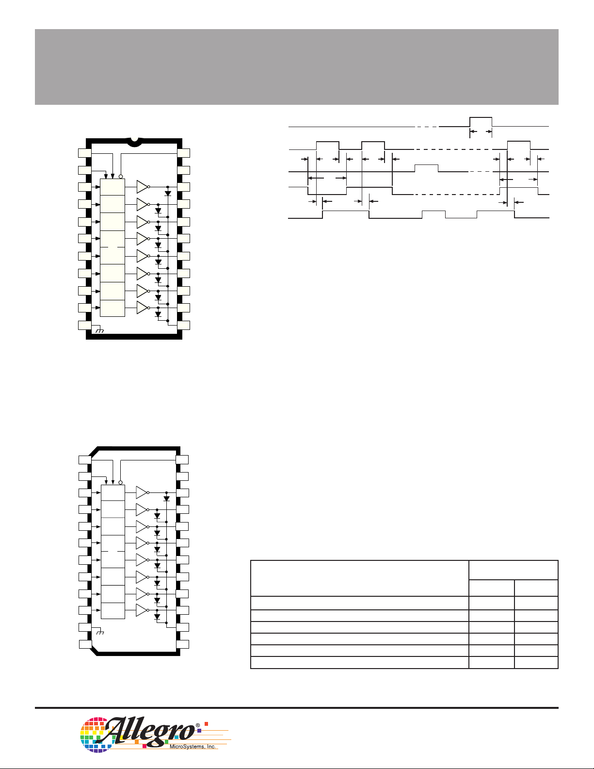
UCN5801A
OUTPUT
1
221
3
1
4
2
5
3
6
4
7
7
5
8
6
9
7
10
8
11
LATCHES
22
ENABLE
V
SUPPLY
DD
20
OUT
1
19
OUT
2
18
OUT
3
17
OUT
4
16
OUT
5
15
OUT
6
OUT
14
7
13
OUT
8
12
COMMON
Dwg. PP-015
UCN5801LW
CLEAR
STROBE
OUTPUT
ENABLE
IN
N
OUT
A
C
BC
G
D
N
B
E
F
C
A
B
G
E
Dwg. No. A-10,895A
TIMING CONDITIONS
(Logic Levels are VDD and Ground)
A.Minimum Data Active Time Before Strobe Enabled
(Data Set-Up Time) ..........................................................50 ns
B.Minimum Data Active Time After Strobe Disabled
(Data Hold Time) ..............................................................50 ns
C.Minimum Strobe Pulse Width ..................................................125 ns
D.Typical Time Between Strobe Activation and
Output On to Off Transition ............................................500 ns
E. Minimum Time Between Strobe Activation and
Output Off to On Transition ............................................500 ns
F. Minimum Clear Pulse Width....................................................300 ns
CLEAR
STROBE
IN
IN
IN
IN
IN
IN
GROUND
CONNECTION
DD
OUTPUT
24
ENABLE
SUPPLY
22
OUT
21
OUT
20
OUT
19
OUT
18
OUT
17
OUT
OUT
16
15
OUT
14
COMMON
NO
13
CONNECTION
1
2
3
4
5
6
7
8
Dwg. PP-015-1
1
223
3
IN
1
4
2
5
3
6
4
7
7
IN
NO
5
8
6
9
7
10
8
11
12
LATCHES
NC
V
NC
G.Minimum Data Pulse Width ..................................................... 225 ns
Information present at an input is transferred to its latch when the
STROBE is high. A high CLEAR input will set all latches to the output
OFF condition regardless of the data or STROBE input levels. A high
OUTPUT ENABLE will set all outputs to the OFF condition, regardless
of any other input conditions. When the OUTPUT ENABLE is low, the
outputs depend on the state of their respective latches.
TRUTH TABLE
OUT
IN
OUTPUT
N
STROBE CLEAR ENABLE t-1 t
0100XOFF
1100XON
XX1XXOFF
X X X 1 X OFF
X 0 0 0 ON ON
X 0 0 0 OFF OFF
X = irrelevant.
t-1 = previous output state.
t = present output state.
115 Northeast Cutoff, Box 15036
Worcester, Massachusetts 01615-0036 (508) 853-5000
N
 Loading...