

DISCONTINUED PRODUCT
— FOR REFERENCE ONLY
Data Sheet
28101.1
STR-S6411
AND
STR-S6411F
These devices are specifically designed to meet the requirements
for increased integration and reliability in off-line flyback (STR-S6411)
and forward (STR-S6411F) converters operating in a fixed-frequency
PWM mode. Each device incorporates the primary control and drive
circuits with an avalanche-rated high-voltage power MOSFET. Crucial
system parameters such as switching frequency and maximum duty
cycle are fixed during manufacture. The STR-S6411 and STR-S6411F
differ only in their maximum duty cycle. Control circuit decoupling and
layout are optimized within each device.
Cycle-by-cycle and average-current limiting, soft start, undervoltage lockout with hysteresis, and thermal shutdown protect the
device during all normal and overload conditions. The performance and
reliability of these devices, and their variable-frequency counterparts,
has been proven in substantial volume production.
The requirements of high dielectric isolation and low transient
thermal impedance and steady-state thermal resistance are satisfied in
an over-molded, 9-pin single in-line power package.
FEATURES
■ PWM Flyback Conversion or Forward Conversion
■ Output Power to 250 W
■ Pulse-by-Pulse Current Limiting
■ Fixed-Frequency 100 kHz PWM
■ Avalanche-Rated Power MOSFET Switch
■ Soft Start
■ Internal Under-Voltage Lockout and Thermal Shutdown
■ Low External Component Count
■ Over-Molded SIP with Isolated Heat Spreader
Always order by complete part number:
STR-S6411 or STR-S6411F .
ABSOLUTE MAXIMUM RATINGS
Supply Voltage, VIN............................ 35 V
Drain-Source Voltage, VDS............... 800 V
Drain Current, I
D
continuous ..................................... ±5 A
single pulse, tw ≤1 ms .................. ±20 A
Avalanche Energy, E
A
single pulse............................... 400 mJ
Gate-Source Voltage, VGS................ ±20 V
Gate-Drive Current Range,
IG................................. -0.7 A to +1.5 A
Over-Current Protection Voltage Range,
V
OCP
............................. -0.3 V to +4.0 V
Insulation RMS Voltage,
V
WM(RMS)
..................................... 2000 V
Package Power Dissipation,
PD........................................ See Graph
FET Channel Temperature, TJ...... +150°C
Internal Frame Temperature, TF... +125°C
Operating Temperature Range,
TA............................... -20°C to +125°C
Storage Temperature Range,
T
stg
............................. -30°C to +125°C
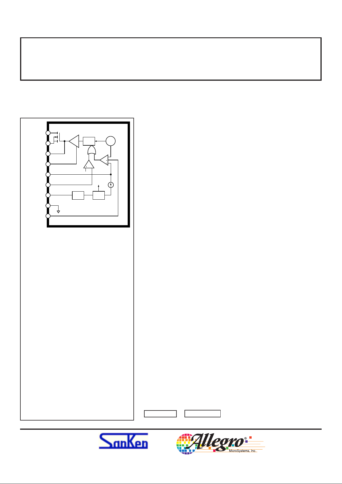
+
SOURCE
DRAIN
UVLO
SIGNAL
GROUND
V
IN
OVER-CURRENT
PROTECTION
Dwg. PK-003
SOFT
START
+
GATE
FDBK
PWM
POWER
GROUND
LATCH
REF.
123456789
OSC.
OFF-LINE SWITCHING REGULATORS
– WITH POWER MOSFET OUTPUT
™
STR-S6411
AND
STR-S6411F
OFF-LINE
SWITCHING REGULATORS
115 Northeast Cutoff, Box 15036
Worcester, Massachusetts 01615-0036 (508) 853-5000
™
FUNCTIONAL BLOCK DIAGRAM
ALLOWABLE PACKAGE POWER DISSIPATION MAXIMUM SAFE OPERATING AREA
OSC.
S
Q
SOURCE
DRAIN
LATCH
1
2
UVLO
SIGNAL
GROUND
4
V
IN
OVER-CURRENT
PROTECTION
R
ton
REF.
7
6
8
Dwg. FK-003
SOFT
START
5
0.2 V
+
GATE
3
FDBK
9
PWM
POWER
GROUND
+
R
toff
R
60
40
20
20 60 100
3.2 W
140
LIMITED BY FRAME
TEMP. = +125°C MAX.
RECOMMENDED MAX.
FRAME TEMP. = +100°C
FREE AIR
62 W
0
TEMPERATURE in °C
ALLOWABLE PACKAGE POWER DISSIPATION in WATTS
MOUNTING SURFACE
TEMPERATURE
Dwg. GK-003
100
10
1.0
0.1
DRAIN-TO-SOURCE VOLTAGE in VOLTS
DRAIN CURRENT in AMPERES
Dwg. GK-004-1
0.3
3.0
30
3.0
10 30 100 300
NO HEAT SINK
NATURAL COOLING
T = +25°C
A
t = 10 ms SINGLE PULSE
w
t = 1 ms SINGLE PULSE
w
1000
t = 0.1 ms SINGLE PULSE
w
LIMITED BY V max
DS
LIMITED
BY r
DS(on)
Copyright © 1994 Allegro MicroSystems, Inc.
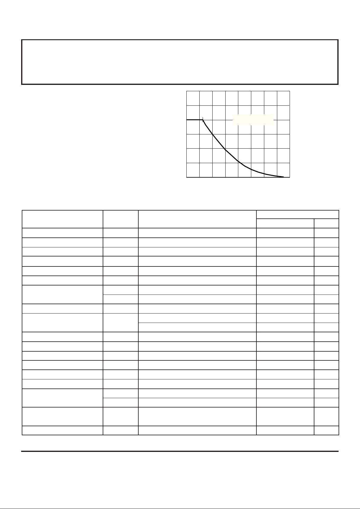
ALLOWABLE AVALANCHE ENERGY
ELECTRICAL CHARACTERISTICS at T
A
= +25°C, VIN = 17 V, voltage measurements are referenced to
Signal Ground (pin 8) (unless otherwise noted).
Limits
Characteristic Symbol Test Conditions Min. Typ. Max. Units
On-State Voltage V
INT
Turn-on, increasing V
IN
14.4 16 17.6 V
Under-Voltage Lockout V
INQ
Turn-off, decreasing V
IN
8.4 9.4 10.4 V
FET Leakage Current I
DSS
VDS = 800 V – – 1.2 mA
FET ON Resistance r
DS(on)
VGS = 10 V, ID = 3 A – 1.8 2.2 Ω
Forward Transconductance g
fs
VGS = 10 V, ID = 3 A 3.0 – – S
FET Input Capacitance C
iss
VDS=10 V, VGS=0 V, f=1 MHz – 1800 – pF
Propagation Delay Time t
phl
Turn-on, 10% VGS to 10% V
DS
–60– ns
t
plh
Turn-off, 90% VGS to 90% V
DS
– 140 – ns
Oscillator Frequency f
osc
93 100 107 kHz
Maximum ON Time t
on
STR-S6411 5.1 5.7 6.5 µs
STR-S6411F 3.8 4.5 5.2 µs
Over-Current Threshold V
OCP(th)
160 200 240 mV
OCP Current I
OCP
-250 -400 -550 µA
Feedback Current I
FDBK
– -1.8 – mA
Soft Start Threshold Voltage V
SS(th)
– – 0.4 V
Soft Start Current I
SS
VSS = 0 V – -100 – µA
Power Ground Current I
PG
tw = 200 ns – -1.0 -1.5 A
Supply Current I
IN(ON)
Operating – 23 – mA
I
IN(OFF)
Start up, VIN = 12 V – – 500 µA
Insulation RMS Voltage V
WM(RMS)
All terminals simultaneous reference 2000 – – V
metal plate against backside
Thermal Resistance R
θJM
FET channel to mounting surface – 2.0 – °C/W
NOTES: Negative current is defined as coming out of (sourcing) the specified device terminal.
Typical Data is for design information only.
600
400
200
0 60 100
140
100
STARTING CHANNEL TEMPERATURE in °C
ALLOWABLE AVALANCHE ENERGY in mJ
Dwg. GK-009-1
300
500
0
20 40 80 120 160
SINGLE PULSE
DRAIN CURRENT = 5 A
SUPPLY VOLTAGE = 50 V
STR-S6411
AND
STR-S6411F
OFF-LINE
SWITCHING REGULATORS
 Loading...